Defect and Electrical Properties of High-κ Dielectric Gd2O3
for Magneto-Ionic and Memristive Memory Devices
by
Sunho Kim
B.S. Materials Science and Engineering
Hanyang University, 2015
Submitted to the Department of Materials Science and Engineering
in partial fulfillment of the requirements for the degree of
Doctor of Philosophy in Materials Science and Engineering
at the
MASSACHUSETTS INSTITUTE OF TECHNOLOGY
September 2020
© Massachusetts Institute of Technology 2020. All rights reserved
Author………
Department of Materials Science and Engineering
August 28, 2020
Certified by………
Harry L. Tuller
R.P. Simmons Professor of Ceramics and Electronic Materials
Thesis Supervisor
Accepted by ………‥
Frances M. Ross
Defect and Electrical Properties of High-κ Dielectric Gd
2O
3for
Magneto-Ionic and Memristive Memory Devices
by Sunho Kim
Submitted to the Department of Materials Science and Engineering on August 27th, 2020 in partial fulfillment of the requirement
for the Degree of Doctor of Philosophy in Materials Science and Engineering
Abstract
While high-κ dielectrics utilized in CMOS technology are noted for their highly insulating characteristics, they have demonstrated surprising electrolytic behavior as key components in a variety of thin film memory devices, including those based on magneto-ionic and memristive behavior. In this work, we focus on the rare earth sesquioxide, Gd2O3, a well-known high-κ dielectric that has exhibited a variety of electrolytic properties during the development and operation of the first magneto-ionic devices developed at MIT. Specifically, we focused our investigation on the defect chemistry and electrical properties of Gd2O3 in order to better understand the relationship between the structure, chemistry, processing conditions, and operating environment and the material’s low-temperature ionic and electronic transport properties and the means for their optimization vis-à-vis memory device operation.
Phase (monoclinic and cubic) and dopant controlled (Ca, Ce, Sr, Zr) polycrystalline pellets of 8 different Gd2O3 systems were prepared to investigate various defect regimes in consideration of this material’s polymorphism. We considered intrinsic anion-Frenkel disorder and electronic disorder, equilibration with the gas phase, water incorporation, and dopant incorporation in the defect modeling, taking into account the roles of crystallographic structure as well as oxygen ion defect and protonic generation. The primary method utilized to characterize the defect chemistry and transport properties of Gd2O3 was the analysis of the dopant, 𝑝𝑂2 and temperature dependencies of the electrical conductivity extracted from complex impedance spectra obtained over the 𝑝𝑂2 range of 1 to 10-15 atm, for 5 isotherms between 700 and 900 ˚C with 50 ˚C steps and for a range of acceptor and donor dopants.
Based on the 𝑝𝑂2 dependency of conductivities, in light of the defect modeling, the majority point defects in each system were identified. Electronic and ionic migration energies and thermodynamic parameters were extracted via the defect modeling and temperature dependencies of conductivities. In nearly all cases, the predominant charge carrier under oxidizing conditions at elevated temperatures was identified as the p-type electron-hole, largely due to oxygen excess non-stoichiometry in these systems. With
decreasing 𝑝𝑂2, transport tended to switch from semiconducting towards ionic. Depending on phase, dopant type & concentration, temperature, and relative humidity, the predominant ionic conductivity was found to be via oxygen interstitials, oxygen vacancies, and/or protons, the latter given by the propensity of Gd2O3 to take up water in solid solution from the environment by the formation of 𝑂𝐻∙species. Unexpectedly, the ionic mobilities of defects in the denser and less symmetric monoclinic system
exhibited higher ionic mobilities than the more open bixbyite structure. The hole electronic species in the investigated systems were found to migrate via the small polaron hopping mechanism with rather large hopping energies. This resulted in an inversion of hole and proton mobility magnitudes at reduced temperatures in the monoclinic system.
Extrapolation of ionic and electronic defect conductivities to near room temperature, based on our derived defect and transport models, was not able to explain, on its own, the observed electrolytic properties of the Gd2O3 thin films utilized in magneto-ionic devices. In an attempt to connect the transport properties obtained under equilibrium conditions at elevated temperatures with the behavior of Gd2O3 near room temperature, selected thin films Gd2O3, prepared by pulsed laser deposition or sputtering, were
investigated by complex impedance spectroscopy over the temperature range of 20 - 170ºC. While films prepared under dry conditions were indeed found to be highly electrically insulating, films exposed to water vapor exhibited dramatically higher proton conductivities (more than ~108 x) than values
extrapolated from high temperature. Parallel thermogravimetric analysis on Gd2O3 powder specimens, as a function of temperature, under high humidity conditions, demonstrated a correlation between
uptake/loss of incorporated water and conductivity upon cooling and heating, respectively. We can therefore conclude that the large disconnect between the electrical and electrolytic properties observed between high-κ dielectrics used in CMOS devices such as Gd2O3, and their much more highly conductive counterparts used in thin film memory devices, depends strategically on the thin film processing
conditions. High-κ dielectrics are fabricated in carefully controlled environments with low relative humidity, while research on, for example, Gd2O3 – based magneto-ionic memory devices, is performed under ambient laboratory conditions, where significant water uptake becomes possible at surfaces and grain boundaries. The results and insights obtained in this study can be expected to be applied in
achieving further progress in the understanding and optimization of magneto-ionic, memristive, and other devices that rely on proton gating.
Acknowledgments
My doctoral study was challenging and enjoyable for me. I could go through the challenges and could enjoy my work thanks to with many smart and nice people.
My thesis advisor, Prof. Harry L. Tuller, was a true advisor in many perspectives. Not only suggesting solutions for the problems I faced, he always encouraged me to think about the solution myself. His training was extremely helpful to enhance my vision and made me more fulfilled as I finish my doctorate. Besides, Thanks to his profound and vast knowledge of ionics made me never be nervous even though I struggled in the early part of my doctorate. Such knowledge leads me to a variety of experience on oxide and I could enjoy the surprise of materials nature. In addition to the academic perspective, as a wise elder, his passion for the science, how he manages himself, how he speaks was impressed me. Once, he told me that not to know currently is fine, however, not to learn is the problem. Due to such his personality, I felt that I got hints about how to live in the future. I’d like to say all the thanks to my thesis advisor, Prof. Tuller.
My thesis committees, Prof. Geoffrey Beach and Prof. Bilge Yildiz, enable me to take a look at my topic in various directions. Their critical comments and advice during my doctorate were very helpful to proceed with my study. I am grateful to my committees for their sincere review of my study. Also, I would like to express my gratitude for Prof. Caroline Ross about sharing her insightful knowledge. I would say I strongly recommend the current graduate students to ask them to be your thesis committee. Working with good people regarded as a great fortune. Working with current and past group members, Thomas Defferriere, Dino Klotz, George Harrington, Han Gil Seo, Dmitri Kalaev, Alexis Grimaud, Tamar Kadosh, Clement Nicollet, Chang Sub Kim, Michael Campion, Kiran Adepalli, and Tobias Huber, were the fortune for me. I could learn a lot from them, could have a better time thanks to them. I sincerely appreciate them for exchanging their ideas and working with me together.
Frankly speaking, collaborating works with Beach group, Aik Jun Tan, Sara Sheffels, Mantao Huang, and Usama Hasan were full of struggles due to the material on my interest. However, my thesis was possible since there were collaboration works with them and I could get a sense of the material. I am thankful to them a lot for going through such a difficult time together. I believe the new findings will lead us to find a remarkable achievement for us in the end.
I am also grateful to the DMSE and MRL staffs, Angelita, Dominique, and Elissa, Mike, James,
Shaymus, Lars, Charlie, Patrick, Timothy, and Libby for their administrative works and for enabling me to make equipment my own and to do characterization.
My Boston life could be more vivid for multiple activities. I’d like to thank the members of TODAM, tennis clubs, KGSA Badminton, and my undergrad alumni community for having a great time with me. I also appreciate the financial support of the National Science Foundation. My study was supported by the MRL as part of the MRSEC Program of the National Science Foundation under grant number DMR-14-19807.
Table of Contents
Chapter 1. Introduction ...17
1.1. Motivation ...17
1.2. Gadolinium Sesquioxide (Gd
2O
3) ...20
1.2.1. Applications of Gd
2O
3...20
1.2.2. Magneto-ionics ...21
1.3. Objectives ...24
Chapter 2. Background ...27
2.1. Rare Earth Oxides: Previous Studies ...27
2.2. Defect Modeling ...31
2.3. Transport of Point Defects ...38
Chapter 3. Experimental Methods ...42
3.1. Ceramic Processing ...42
3.2. Thin Film Deposition ...43
3.2.1. Sputter Deposition ...43
3.2.2. Pulsed Laser Deposition (PLD) ...44
3.3. Physical Characterization ...45
3.3.1. X-Ray Diffraction (XRD)...45
3.4. Electrical Characterization ...47
3.4.1. Electrochemical Impedance Spectra (EIS) ...47
3.4.2. Cyclic Voltammetry (CV) ...50
Chapter 4. Result ...53
4.1. Bulk Polycrystalline Defect Chemistry and Electrical Property ...53
4.1.1. Composition Selection...53
4.1.2. Structure Analysis ...55
4.1.3. Electrical Conductivity ...58
4.2. Thin Film Gd
2O
3Electrical Measurement near Room Temperature ...65
4.2.1 Sample Design ...65
4.2.2. Electrical Conductivity Measurements near Room Temperature ...70
4.2.3 Thermogravimetry Analysis of Gd
2O
3near Room Temperature ...76
Chapter 5. Discussion ...81
5.1. Defect Chemistry and Electrical Properties of Gd
2O
3...81
5.1.1 Monoclinic Samples ...83
5.1.2 Cubic Samples ...92
5.1.3 Interpretation ...100
5.2. Proton Conductivity of Thin Film Gd
2O
3near Room Temperature ...106
5.2.1 Proton Conducting Mechanism near Room Temperature of YSZ ...106
5.2.2. Temperature-Dependent Water/Proton Concentration ...109
5.2.3. Analysis of Conductivity Measurements near Room Temperature ...111
Chapter 6. Conclusion ...121
6.1. Summary ...121
6.2. Outlook ...126
List of Figures and Tables
Figures
Figure 1.1. Market demand increase for data storage in North America. Reprinted from reference. [2] Figure 1.2. Structure of NVRAMs (a) FeRAM [3], (b) STT-MRAM [4], (c) PCRAM [5], and (d) RRAM [6]. Reprinted from references.
Figure 1.3. Structure of the magneto-ionic device. Reprinted from reference. [15]
Figure 1.4. Mechanism of magneto-electric effect. Reprinted from the thesis of Bauer, U.. [31]
Figure 1.5. EELS on magneto-ionic device under gating in GdOx. Oxygens migrate from and to Co layer. Reprinted from reference. [16]
Figure 1.6. The operation of protonic magneto-ionic device. Protonation of Pd happens due to proton conduction in GdOx. Reprinted from reference. [15]
Figure 2.1. Polymorphism of rare earth sesquioxides. Reprinted from reference. [36]
Figure 2.2. Crystal structures of B and C phase of rare earth sesquioxides. Reprinted from reference. [36]. Figure 2.3. Electrical conductivity in nS/cm versus 1000/T in 1/K. The conductivities are of Sm2O3, Eu2O3, and Yb2O3 referenced from the top curve. Reprinted from reference. [42]
Figure 2.4. Proton conductivity of various acceptor doped oxides under humid environments. Reprinted from reference. [45]
Figure 2.5. Defect diagram showing 𝑝𝑂2 dependence for acceptor doped case under low humidity. Figure 2.6. Defect diagram showing 𝑝𝑂2 dependence for donor doped case under low humidity. Figure 2.7. Defect diagram showing 𝑝𝑂2 dependence for acceptor doped case under high humidity. Figure 2.8. Defect diagram showing 𝑝𝐻2𝑂 dependence for acceptor doped case under high humidity and intermediate to low 𝑝𝑂2.
Figure 2.9. Schematic of Grotthuss mechanism. Reprinted from reference. [62]
Figure 3.1. Flow chart of ceramic processing used in this study.
Figure 3.2. (a) A schematic of sample with MIM structure. (b) photo of device structure after each preparation step.
Figure 3.3. Thin film deposition techniques. (a) sputtering (b) pulsed laser deposition.
Figure 3.4. An example of the Nyquist plot from EIS of a solid with grain/grain boundary/electrode contributions. Reprinted from reference. [63]
Figure 3.5. An example of the Nyquist plot from EIS of a solid with grain/grain boundary/electrode contributions. Reprinted from reference. [64]
Figure 3.6. Examples of cyclic voltammetry curves relevant to Randles-Sevcik relation. Reprinted from reference. [71]
Figure 4.1. A representative SEM image of pellets.
Figure 4.2. X-ray diffraction patterns of specified samples. (a) monoclinic samples (b) cubic samples. Figure 4.3 Oxygen density dependence of 𝐻𝑊 for a variety of oxides with fluorite and perovskite related structures. Diagonal across bottom of left to the top of the right is relevant to monoclinic and the other diagonal is relevant to bixbyite. Reprinted from the reference. [55]
Figure 4.4. Examples of impedance spectra taken for C-Ce0.2Gd1.8O3.1+δ as a function of log pO2 at T = 795 ˚C.
Figure 4.5. Measured total conductivity isotherms (symbols) and their fittings (dash lines) of (a) B-Gd2O3+δ and (b) B-Ca0.2Gd1.8O2.9+δ.
Figure 4.6. Measured total conductivity isotherms (symbols) and their fittings (dash lines) of (a) B-Sr0.04Gd1.96O2.98+δ and (b) B-Zr0.04Gd1.96O3.02+δ.
Figure 4.7. Measured total conductivity isotherms (symbols) and their fittings (dash lines) (a) C-Gd2O3+δ and (b) C-Ca0.04Gd1.96O2.98+δ.
Figure 4.8. Measured total conductivity isotherms (symbols) and their fittings (dash lines) (a) C-Zr0.04Gd1.96O3.02+δ and (b) C-Ce0.2Gd1.8O3.1+δ.
Figure 4.9. 2Θ-ω scan X-ray diffraction pattern (a) and the rocking curve of (402̅) plane (b) of B-Ca0.04Gd1.96O2.98+δ film deposited by PLD.
Figure 4.11. Cross-section TEM of GdOx used in references. [14,34] by courtesy of A. J. Tan and M. U. Hasan, MIT, and D. Wolf, IFW Dresden.
Figure 4.12. Examples of impedance spectra obtained for a MIM cell with B-Ca0.04Gd1.96O2.98+δ as the I component; modeled as a (a) resistor, (b) small RC circuit, (c) large RC circuit, and (d) capacitor. Figure 4.13. The conductivity of a MIM cell with B-Ca0.04Gd1.96O2.98+δ as the I component exhibiting (a) Resistor Type (Figure 4.12a) impedance and (b) RC Type impedance defined in the paragraph upon heating and cooling.
Figure 4.14. An example of a room temperature impedance spectra of a MIM cell (I = GdOx) and equivalent circuit obtained on cell from the Beach group.
Figure 4.15. Example of DRT spectra obtained on cells of the type measured in Fig 4.14 at temperatures from 23 to 170ºC.
Figure 4.16. Conductance of MIM cells with GdOx obtained from Beach group near room temperature in laboratory air. (a) Pt top electrode and (b) Au top electrode cases.
Figure 4.17. (a) precursor powder of a green pellet for the nano-crystalline gadolinia. (b) hydration (saturation) process of nano-sized crystalline green pellet.
Figure 4.18. TGA of micro-sized crystalline (a) B-Ca0.04Gd1.96O2.98+δ and (b) C-Gd2O3+δ. Figure 4.19. TGA of nano-crystalline C-Gd2O3.
Figure 5.1. Analyzed temperature dependence of conductivity contributions of B-Gd2O3+δ. (a)
Temperature dependence of fitted p-type conductivity contribution. (b) Temperature dependence of ionic conductivity.
Figure 5.2. Analyzed temperature dependence of fitted parameters of B-Ca0.2Gd1.8O2.9+δ. (a) Temperature dependency of the fitted parameter 𝛼. (b) Temperature dependency of the fitted parameter 𝛽. (c)
Temperature dependency of ionic conductivity.
Figure 5.3. Analyzed temperature dependency of B-Sr0.04Gd1.96O2.98+δ. (a) Temperature dependence of fitted p-type conductivity contribution. (b) Temperature dependence of ionic conductivity.
Figure 5.4. (a) Temperature dependence concentration of hydroxide ions, oxygen vacancies, and holes in the defect regime in which acceptors are compensated by vacancies and hydroxide ions. The
pre-exponential coefficients of the equilibrium constants were chosen arbitrarily based on % range doping and estimable values of 𝐾𝑂0 and 𝐾𝑊0 values from this study and reference. [54] (b) make-up conductivity measurement to the lower temperatures.
Figure 5.5. Analyzed temperature dependence of fitted parameters of B-Zr0.04Gd1.96O3.02+δ. (a)
Temperature dependence of fitted parameter 𝛼. (b) Temperature dependence of fitted parameter 𝛽. (c) Temperature dependence of fitted parameter 𝛾.
Figure 5.6. Analyzed temperature dependence of fitted parameters of C-Gd2O3+δ. (b) Temperature dependence of fitted parameter 𝛼. (c) Temperature dependence of fitted parameter 𝛽.
Figure 5.7. Analyzed temperature dependence of fitted parameters of C-Ca0.04Gd1.96O2.98+δ. (a) Temperature dependence of fitted 𝐾𝐻𝑝𝐻2𝑂
1
2 (b) Temperature dependence of ionic conductivity.
Figure 5.8. Analyzed temperature dependence of fitted parameters of C-Zr0.04Gd1.96O3.02+δ. (a) Temperature dependence of p-type conductivity contribution. (b) Temperature dependence of ionic conductivity.
Figure 5.9. Analyzed temperature dependence of fitted parameters C-Ce0.2Gd1.8O3.1+δ. (a) Temperature dependence of fitted n-type conductivity contribution. (b) Temperature dependence of ionic conductivity. Figure 5.10. Temperature dependence of hole, oxygenic defect, and proton mobilities in (a) B-Gd2O3 (b) C-Gd2O3
Figure 5.11. (a) Four kinds of water physisorption and chemisorption shown schematically in YSZ, (b) temperature-dependent thermal desorption spectroscopy (TDS) results, (c) temperature-dependent conductivity measurements under H2O and D2O conditions, and (d) temperature dependence of proton conductivity of various oxides. Reprinted from reference. [76]
Figure 5.12. Proton/water open-pore conduction model in oxides, Gregori, G. et al. [88], and the relevant equivalent circuit by Stub, S. Ø . et al. [89] Reprinted from the references.
Figure 5.13. Schematic summarizing proton conducting mechanisms in Gd2O3 as a function of degrees of water absorption. Top image illustrates the increasing hydration of boundaries between columnar grains with increasing water absorption.
Figure 5.15. Temperature dependence of proton conductivity of a textured B-Ca0.04Gd1.96O2.98+δ thin film under a variety of hydration levels The green and yellow lines are the extrapolated lines from the Sr 2% doped monoclinic and Ca 2% doped cubic polycrystalline oxide pellets in this study.
Figure 5.16. Various microstructural changes induced upon hydration/dehydration and heating/cooling in MIM sample with the model oxide layer. The cell was hydrated at room temperature (wet N2) and heated (300 ˚C) and cooled without electrical testing. This sample was deposited identically to the sample that we used in electrical measurements, but on Si (001) as a substrate.
Tables
Table 2.1. The defect regimes in Gd2O3 systems depending on 𝑝𝑂2 and 𝑝𝐻2𝑂.
Table 2.2. The analytic solutions of point defect concentrations in each defect regime of Gd2O3 systems. Table 4.1. Investigated systems and the ionic radii of the dopants. Ionic radii were taken from reference. [72]
Table 4.2. The fitted lattice parameters and calculated oxygen densities of investigated gadolinias. Table 4.3. Calculated HW values based on extrapolation from the reference [55,56] and extracted oxygen site density in Table 4.2.
Table 5.1. Summary of fitted parameters in B-Gd2O3 systems.
Table 5.2. Extracted thermodynamic and kinetic parameters of B-Gd2O3 systems. Values with ~ indicate rough estimation. Values with * are from reference [55]. Energies in 𝑒𝑉, mobility coefficients in
𝐾𝑐𝑚2/𝑉𝑠.
Table 5.3. Summary of fitted parameters in C-Gd2O3 systems.
Table 5.4. Extracted thermodynamic and kinetic parameters of C-Gd2O3 systems. Values with ~ indicate rough estimation. Energies in 𝑒𝑉, mobility coefficients in 𝐾𝑐𝑚2/𝑉𝑠.
Table 5.5. Summary of relevant defect regimes and identify of majority conducting defects in monoclinic gadolinia at the investigated conditions.
Table 5.6. Summary of relevant defect regimes and identify of majority conducting defects in cubic gadolinia at the investigated conditions.
Chapter 1. Introduction
1.1. Motivation
Since the advent of integrated circuits (IC), semiconductor devices have been an essential technology in modern society, offering humanity increased productivity, convenience, and entertainment in
unimaginable ways. As the demands on computation have increased, so has the demand for better hardware offering higher speed, lower cost and size, reduced power requirements, and much increased data storage capacity. The growth in data generation is growing exponentially. For example, a 2013 report pointed out that the data produced in the past two years already represented 90% of the total data produced to date. [1] The reasons are multiple, including the development of smartphones that computers have become mobile, and the computers that allow people to start to share information via video along with text and image. The recent development of artificial intelligence (AI) technology, such as deep learning, demands huge data sets, requiring the establishment of data servers and centers. Increased demand for data storage can be expected to continue for at least the next decades in support of self-driving vehicles. This will all require improved primary data storage with better random-access speed, and low-power components that enhance the duration of mobile applications. All these points to increasing demands for inexpensive, fast, low power, and very high capacity data storage.
Non-volatile random-access memory (NVRAM) is an ideal data storage device concept. Conceptually, NVRAM should be non-volatile (maintain a state for years), high density, simple to fabricate, low cost, with high switching speeds over countless cycles, and low power consumption. To describe the current structure of data storage, the storage technologies can be categorized as primary and secondary storage. Static random-access memory (SRAM) and dynamic random-access memory (DRAM) are primary storage media, while hard disk drive (HDD) and flash memory are secondary storage. For computation, there is no fundamental reason that the storage needs to be separated into two types, other than
technological challenges. Each type of data storage presently has complementary advantages and disadvantages. Primary storage is swift but volatile and difficult to fabricate. Secondary storage is non-volatile and dense in capacity, but sluggish. Therefore, trials to simplify computing structure via
developing NVRAM have been attempted, and widely researched for decades. For example, Ferroelectric RAM (FeRAM), spin-transfer torque magnetic RAM (STT-MRAM), phase-change RAM (PRAM), and resistive RAM (RRAM) have been investigated as NVRAM concepts, some of which have reached a level of commercialization. [3-7] However, such new commercialized storage concepts still possess problems such as high cost and limited capacities.
Figure 1.2. Structure of NVRAMs (a) FeRAM [3], (b) STT-MRAM [4], (c) PCRAM [5], and (d) RRAM [6]. Reprinted from references. (Copyright by Nature Research [3, 6], Elsevier [4], and IBM [5])
The NVRAM concepts are usually based on a developed version of existing data storage. FeRAM and STT-MRAM harness materials hysteresis similar to HDD and recording tape, and phase change concept of PRAM is analogous to Blue-ray laser discs. The operation mechanism of RRAM or memristor, a device developed a decade ago, is rather unconventional. Memristors consist of a metal/insulator/metal (MIM) structure that switch their resistance state due to ion redistribution, locally or universally in the oxide, under the application of high fields. [8] While ion redistribution is normally disregarded under ambient temperatures due to exceedingly low mobilities, potentials applied across the extremely thin dielectric layer between the two electrodes can induce massive electric fields, and this induces ionic migration even at room temperature. With this mechanism, surprisingly, RRAM could satisfy the performance criteria of NVRAM if one focuses only on the best performances reported in the literature. [9-14] Generally, however, NVRAM devices suffer from reproducibility issues, with switching sensitive to the oxide layer microstructure and composition. [11-14]
Figure 1.3. Structure of the magneto-ionic device. Reprinted from reference. [15] (Copyright by Nature Research)
and rely on field-driven ionic migration in the oxide layer as do memristors. Potential advantages over conventional memristors include 1) ability to toggle magnetization, a conventionally applied property for memories, 2) magnetic switching is less susceptible to side contributions than resistance switching, and 3) switching occurs uniformly across the area of the device. Such devices can potentially be applied as components in MRAM, with switching having the potential to be more reproducible than memristors, while being energetically efficient like memristors.
Like the other NVRAM technologies, this device also has limitations. Speed is slow, with limited information regarding the details of operation (electrochemistry). [15,16] In this thesis, we focused our attention on a key essential component of these newly developed devices, i.e., the electrolyte, Gd2O3.
1.2. Gadolinium Sesquioxide (Gd
2O
3)
1.2.1 Applications of Gd
2O
3Lanthanide oxides are high-κ dielectric materials and have been replacing SiO2 in CMOS technology as the dimensions of MOSFETS have continued to shrink in dimensions to below 10 nm. Gd2O3 has a large band gap, good chemical and thermodynamic stability, and large resistivity compared to the many of the other lanthanide oxides. Consequently, it has been seriously considered to serve as the high-κ dielectric for CMOS applications. [17-19] However, it was been displaced by HfO2 that exhibits better stability and a larger dielectric constant.
Lanthanide elements have also been popular ingredients of phosphor materials given multiple optical transitions between their partly filled 4f-orbital states. As a lanthanide compound, Gd2O3 offers high solubility to the other lanthanide ions along with good thermodynamic stability and a large band gap, and has therefore been of interest as a host matrix for lanthanide ion-based phosphors. [20,21]
Gd is an f-block (lanthanide) element, with the Gd3+ ion possessing the highest spin moment (+7/2). Thanks to the spin moment, biologically safe materials containing Gd3+ have been used as contrast agents for MRI. As one of the most energetically favored compounds containing Gd3+, the nanoparticles of Gd2O3 are also used as contrast agents for MRI. Besides, modified nanoparticles are under research as multifunctional contrast agents. [22,23]
Overall, the conventional applications of Gd2O3 have harnessed its insulating properties and thermal and chemical stability. However, a totally different story emerges when the properties of Gd2O3 are examined in light of its use in magneto-ionic devices.
1.2.2 Magneto-ionics
The magnetism of the Co layer in a magneto-ionic device correlates with field-induced ionic motion. To understand the ionic transport properties better, the magnetization of the Co layer is introduced below. The material’s directional dependence on magnetism, magnetic anisotropy, is an important consideration in applications of magnetic materials since the energy required to magnetize the material depends on the direction of the applied field and the easy magnetization axis of magnetic anisotropy. [24] In data storage using ferromagnets, the data storing media has the shape of thin films and with a preferred easy axis directing out-of-plane direction or to have perpendicular magnetic anisotropy (PMA) since this can increase data capacity and decrease energy consumption. [25, 26] The magnetic anisotropy depends on the material’s shape, interface/surface, and volume. In thin film shape, the interface contribution tends to reinforce PMA and the volumetric contribution tends to remove PMA. Therefore, thin films can exhibit PMA when the film is thin enough and is combined with interfaces favoring PMA. [24] For example, Co/noble metal (Au, Pt, and Pd) bilayers and Co/oxides (AlOx, MgO, TaOx, and GdOx) thin films are systems known for favoring PMA due to strong interface anisotropy. [27-30] This is caused by the hybridization of orbitals (Co 3d with the d orbital of a noble metal or Co 3d with 2p orbital of oxygen, respectively). The hybridizations split the Co bands, and this modifies the electronic filling of the 3d-band in the direction of favoring PMA. Therefore, the noble metal/Co/oxide thin film structure, which is the key part of the magneto-ionic device, is a system that can drive strong PMA.
As hybridization of the Co 3d orbital with the orbitals of materials above and beneath it could enhance PMA, disturbing the hybridization can result in the decay of PMA. During the switching process, the electrical potential is applied across the dielectric or electrolyte layer. When the oxide layer acts as a dielectric layer, we should consider this a magneto-electric effect. If the oxide acts as an electrolyte, we should consider the coupling between Co and ions, i.e. as an electrochemical reaction.
Figure 1.4. Mechanism of magneto-electric effect. Reprinted from thesis of Bauer, U.. [31] (Copyright by Massachusetts Institute of Technology)
The magneto-electric effect is a coupling between magnetization and electric fields. When we regard GdOx as a dielectric layer, one of the magneto-electric couplings can be relevant to magneto-ionic features. An applied field can accumulate/deplete charges at the interfaces of the electrode and magnetic layer with the dielectric layer (Figure 1.5). This charge accumulation/depletion can change the filling of Co 3d-band and this can result in weakening and strengthening of PMA. [30,32]
Figure 1.5. EELS on magneto-ionic device under gating in GdOx. Oxygens migrate from and to Co layer.
However, this magneto-electric effect turned out to be not an energetically efficient means of switching. According to Bauer et al., initially developed magneto-ionic devices exhibited more than 50 times more energetically efficient magnetization switching than that of the magneto-electric devices. [16] In the reported device, magnetization switching occurs via oxidation and reduction of the Co layer. In other words, a ferromagnetic Co layer could be converted into paramagnetic CoO via an electrochemical redox reaction, and vice versa. Electron energy loss spectroscopy (EELS) spectra in Figure 1.5 shows evidence of oxygen transport in the reaction. We can conclude that GdOx functioned as an oxygen electrolyte in this system. Qualitative parameter dependencies such as thickness, temperature, and availability of gas exchange also support this.
Figure 1.6. The operation of protonic magneto-ionic device. Protonation of Pd happens due to proton conduction in GdOx. Reprinted from reference. [15] (Copyright by Nature Research)
4 years after the report by Bauer et al. of an oxygen ion-based magneto-ionic effect, Tan et al. reported a proton-based magneto-ionic effect device. They showed that the devices with an identical structure to the
consistent with a study by C. R. Abeledo et al., that showed that chemisorption of hydrogen on cobalt can decrease the magnetic moment of Co. [33] These observations demonstrated that the GdOx layer can act as a proton reservoir or electrolyte.
The magneto-ionic device has the potential to be a highly compact and energy-efficient memory
component for future MRAM technology. GdOx (or Gd2O3), the initial electrolyte choice for the device, appears to exhibit properties as an oxygen or proton electrolyte. Combining the fact that Gd2O3 also serves as a high-κ dielectric, the magnetization of the initially proposed magneto-ionic device could in principle be affected by all three-effects introduced above. In that sense, investigating the properties of Gd2O3 should be highly interesting given the wide range and variety of electrical properties that it apparently exhibits and applicable towards understanding and optimizing magneto-ionic and memristive devices utilizing Gd2O3.
1.3. Objective
In the emerging market for novel memory devices, we regard the dielectric/electrolyte layer as a key component for further development of memristive and magneto-ionic devices. Gd2O3 exhibited insulator and electrolyte duality in previous studies. In support of understanding the property duality of Gd2O3, it becomes essential to investigate the defect chemistry and its impact on the electrical properties of Gd2O3. The defect chemistry will tell us how the point defect or charge carrier concentrations inside the material can be controlled depending on the atmosphere, temperature, and dopants. Since there has been limited research on the defect chemistry of Gd2O3, this study begins with an investigation of the bulk properties at elevated temperatures. In oxides, the defect and electrical properties at elevated temperatures do not always correlate simply with the properties at lower temperatures. This stems from the following reasons: the key thermodynamic parameters can change over the wide temperature range, ionic defect association occurs at lower temperatures, and at a lower temperature the materials rarely reach equilibrium with the environment. The information gained, however, is essential for projecting what properties can be expected and what approaches can be taken to adjust materials properties during sample preparation and subsequent quenching or annealing. By investigating doped materials further extend properties by inducing the formation of various types of defects and thereby influencing both the mass transport and electronic properties of the material.
In short, the objective of this study is to suggest approaches for tailoring Gd2O3 for multiple applications including as an oxygen ion or proton electrolyte on the one hand or a highly insulating high-κ dielectric
on the other. Another main objective is making a correlation between the elevated temperature studies and properties of room temperature devices. Based on the investigated defect model and transport properties, we chose compositions that can exhibit distinctive differences compared to undoped gadolinia. In particular, as we found a composition that can work as a proton electrolyte, we focused more on the verification of the electrolytic function of the oxide. Thin films of the chosen composition were deposited as a sandwiched layer in metal/insulator/metal (MIM) structure as in memristors and their electrical properties were examined via electrochemical methods. The experiment was conducted under humid and dry atmospheric conditions near room temperature. Here, we expected to observe the characteristics of devices from the MIM structure. This structure was also regarded as a structure facilitating correlations between results of elevated temperature research and the room temperature behavior of the oxide. Other than resistive switching and magnetic switching, recently developed devices using field-driven ionic migration exhibit variety in switching behavior such as light absorption or thermal conductivity. [34, 35] However, there are limitations such as cyclability and speed. For further enhancement of such properties, other electrolyte or electrolyte/electrode combinations may need to be investigated.
Chapter 2. Background
2.1. Rare Earth Oxides: Previous Studies
Before discussing Gd2O3 in detail, it is useful to first discuss the properties of rare earth sesquioxides more generally. As an oxide having a cation with f-orbital valence electrons, Gd2O3 has many siblings with similar properties. Since the transport properties of Gd2O3 has not been widely researched, it becomes useful to examine similar properties reported for the related rare-earth sesquioxides.
Figure 2.1. Polymorphism of rare earth sesquioxides. Reprinted from reference. [36] (Copyright by Elsevier)
First, rare earth sesquioxides exhibit polymorphism. As shown in Figure 2.1, solid-state rare earth sesquioxides can exist as C (cubic), B (monoclinic), A (Hexagonal), H (Hexagonal), and X (Cubic) phases. [36] While the phase diagram for these systems is well established, phases achieved following processing may be different from expectations based on such diagrams given the likelihood of obtaining metastable phases. Thus, phase identification is crucial when one proceeds to research these systems.
temperature phases and it could appear when RE2O3 is deposited as a thin-film given appropriate lattice matching with the substrate. The H and X phases are difficult to observe since these are only stable over 2000 ˚C, and so likely have significant differences in Gibbs free energy with those of the equilibrium phases at lower temperatures. For the Gd2O3 case, the C phase Gd2O3 (C-Gd2O3) is the equilibrium state at room temperature, however, the B phase Gd2O3 (B-Gd2O3) (Structures are shown in Figure 2.2) can also exist metastably at room temperature regardless of whether it is in powder, pellet, or thin film form. This can be attributed to the small difference in formation enthalpy (~9 KJ/mol) between the C and B Gd2O3 phases. [36,37]
Figure 2.2. Crystal structures of B and C phase of rare earth sesquioxides. Reprinted from reference. [36] (Copyright by Elsevier)
Most rare earth sesquioxides are insulators. According to a first principle simulation, the band gap between the O 2p and RE 4d derived bands is larger than 5 eV, and if there is a 4f-band that fall inside this band gap, the effective band gap can be smaller than 5 eV. [37, 38] This is supported by experimental results characterized with respect to their UV-Vis spectra. [39] As a well-known insulator, the band gap of Gd2O3 is over 5 eV [40-41]. According to theoretical calculations, the 4f-band of Gd2O3 splits to components deep inside of the valence and conduction bands, resulting in no internal band and thereby a large band gap. [38]
Figure 2.3. Electrical conductivity in nS/cm versus 1000/T in 1/K. The conductivities of Sm2O3, Eu2O3,
and Yb2O3 referenced from the top curve. Reprinted from reference. [42] (Copyright by Elsevier)
Given a very large band gap, one does not expect significant semiconducting property in these materials. The electrical conductivities of rare-earth sesquioxides have been investigated only sporadically over the decades, given their low conductivity. Figure 2.3 shows reported electrical conductivities measured for Sm2O3, Eu2O3, and Yb2O3 as a function of reciprocal temperature confirming their rather insulating properties. [42] According to this work, the RE2O3 (RE: La, Pr, Nd, Sm, Eu, Gd, Tb, Ho, Yb, and Y in this study) with equilibrium phases below 900 ˚C exhibit thermally activated conductivities with a large p-type contribution in air. As shown in Figure 2.3, the magnitude of conductivity is in the semiconducting range at higher temperatures but becomes highly insulating near room temperature.
Each oxide commonly exhibits an activation energy transition in the measured temperature range. Partial ionic conduction observed at elevated temperature has been suggested to be the source of the transition. Alternatively, given the relatively low temperature of the transition, another possibility is that it can be the result of sluggish gas exchange in the oxide at reduced temperatures. K. H. Kim et al. and J. S. Choi et al. measured the conductivity of Sm2O3 and Tm2O3, respectively, as a function of temperature and oxygen partial pressure. [43,44] In their result, the conductivity of the material exhibited a power-law dependence on 𝑝𝑂2 with slope ~1/6 (or 3/16) indicating stoichiometry dependent p-type conduction above 400 - 1000
Figure 2.4. Proton conductivity of various acceptor doped oxides under humid environments. Reprinted from reference. [45] (Copyright by Annual Reviews)
Another possibility is the intervention of protonic conduction. Most of RE2O3s are known to be hygroscopic, meaning that they can accommodate a significant number of hydroxide ions by absorbing water from the environment. Not surprisingly, some acceptor doped RE2O3s are fair proton ion
conductors, and Ca:Nd2O3 even has comparable conductivities with perovskite proton conductors as shown in Fig 2.4. [45] Due to the high proton conductivity (and mobility), the related defect chemistry of these materials is relatively well-described. [46-51] There are two notable trends. First, the protonic mobilities are largely phase-dependent; the A phase is the best, while the C phase is the worst. Second, A and B phase sesquioxides share an oxygen density dependency of the enthalpy of the water incorporation reaction (to discussed in the next section) with perovskite oxides. However, the C phase sesquioxide shares the oxygen density dependency with fluorite oxides.
Based on our review of the properties of RE2O3, we summarize some key considerations in investigating the defect chemistry and electrical properties of Gd2O3. 1) Gd2O3 has polymorphism and the C→B phase transformation is irreversible, 2) Gd2O3 has a very large electronic band gap, 3) the magnitude of
electrical conductivity is quite low, and this can be due to mixed p-type and ionic contributions 4) small polaron hole hopping is expected, and 5) protonic conduction can be predominant at higher temperatures. In this study, the experimental design and defect modeling were selected based on these considerations.
2.2. Defect Modeling
Defect modeling is a powerful method to anticipate the defect chemistry of a system under targeted conditions. The modeling includes defect reactions composed of dominant point defect concentrations and external variables such as oxygen partial pressure and temperature. Such defect reactions include intrinsic ionic and electronic disorders, and gas exchange reactions. As an intrinsic ionic disorder, possible reactions include anion Frenkel disorder, cation Frenkel disorder, and Schottky disorder. Based on earlier simulation work, anion Frenkel disorder is the predominant intrinsic ionic reaction in C-Gd2O3. [51] This is an expected result given that anion Frenkel disorder is the major intrinsic ionic disorder reaction in CeO2, with a related RE oxide structure. by similar logic, we assumed that the predominant intrinsic ionic disorder is anion Frenkel disorder in B-Gd2O3. Applying Kröger-Vink notation, and given equilibrium constant (𝐾𝐹), enthalpy (𝐻𝐹), and entropy (𝑆𝐹) for Frenkel pair generation, the anion Frenkel disorder reaction can be formulated as:
𝑂𝑂× ⇌ 𝑉 𝑂∙∙ + 𝑂𝑖′′ 𝐾𝐹(𝑇) = exp (− 𝐻𝐹 𝑘𝑇+ 𝑆𝐹 𝑘) = [𝑉𝑂∙∙][𝑂 𝑖′′] [𝑂𝑂×] ⋯ (2.1) where 𝑂𝑂𝑋, 𝑉
𝑂∙∙ and 𝑂𝑖′′ are oxide ions on oxygen sites, doubly positively charged oxygen vacancies on oxygen sites, and doubly negatively charged oxygen interstitials, respectively.
All materials with a band gap, exhibit intrinsic electronic disorder. With equilibrium constant (𝐾𝑒), bandgap (𝐸𝑔), and density of states in the conduction band (𝑁𝐶) and valance band (𝑁𝑉) respectively, the reaction can be expressed as:
𝑛𝑢𝑙𝑙 ⇌ 𝑒′ + ℎ∙
𝐾𝑒(𝑇) = 𝑁𝐶𝑁𝑉exp (− 𝐸𝑔
𝑘𝑇) = 𝑛𝑝 ⋯ (2.2) where n and p are the concentration of electrons and holes, respectively.
As explained above, we need to count two different gas exchange reactions since the defect chemistry of Gd2O3 is cross sensitive to both oxygen and water vapor. One is responsible for oxygen exchange and the other is responsible for proton (water vapor) exchange. There are multiple ways to express these
1 2𝑂2(𝑔) + 𝑉𝑂 ∙∙ ⇌ 𝑂 𝑂× + 2ℎ∙ 𝐾𝑂(𝑇) = exp (− 𝐻𝑂 𝑘𝑇+ 𝑆𝑂 𝑘) = [𝑂𝑂×]𝑝2 [𝑉𝑂∙∙]𝑝𝑂 2 1 2 ⋯ (2.3)
where 𝐾𝑂, 𝐻𝑂 and 𝑆𝑂 are the equilibrium constant, enthalpy, and entropy of the oxidation reaction, respectively. Two ways have been used to express water vapor exchange reactions involving holes vs oxygen vacancies. With the equilibrium constant, enthalpy and entropy of the relevant reactions, proton incorporation reaction via holes (noted by H) and via vacancies (noted by W) can be defined as:
1 2𝐻2𝑂(𝑔) + ℎ ∙ + 𝑂 𝑂× ⇌ 𝑂𝐻𝑂∙ + 1 4𝑂2 𝐾𝐻(𝑇) = exp (− 𝐻𝐻 𝑘𝑇+ 𝑆𝐻 𝑘) = [𝑂𝐻𝑂∙]𝑝𝑂 2 1 4 𝑝[𝑂𝑂×]𝑝𝐻2𝑂12 ⋯ (2.4) 𝐻2𝑂(𝑔) + 𝑉𝑂∙∙ + 𝑂𝑂× ⇌ 2𝑂𝐻𝑂∙ 𝐾𝑊(𝑇) = exp (− 𝐻𝑊 𝑘𝑇 + 𝑆𝑊 𝑘 ) = [𝑂𝐻𝑂∙]2 [𝑉𝑂∙∙][𝑂 𝑂×]𝑝𝐻2𝑂 ⋯ (2.5)
where 𝑂𝐻𝑂∙ is hydroxide ion on an oxygen site, where the hydroxide ions are the source of proton conduction in the material.
In addition to the intrinsic reactions introduced above, this study aims to suggest how to tailor Gd2O3 for various applications including magneto-ionic devices. One of the representative methods of tailoring oxides is by doping. We consider both M2+ acceptor and M4+ donor doping. With the addition of AO and DO2, the relevant reactions, depending on the 𝑝𝑂2, can be expressed as:
2𝐴𝑂 ⇌ 2𝐴𝐺𝑑′ + 2𝑂𝑂𝑋+ 2ℎ∙ 𝑜𝑟 𝑉 𝑂∙∙ 2𝐷𝑂2 ⇌ 2𝐷𝐺𝑑∙ + 3𝑂𝑂×+ 2𝑒′ 𝑜𝑟 𝑂𝑖′′
where 𝐴𝐺𝑑′ is acceptor cation and 𝐷𝐺𝑑∙ is donor cation on Gd3+ sites respectively. Depending on the defect regime, compensation can occur either by ionic or electronic defects.
The total charge of the material is invariant unless reaction with charged matter occurs. Summing all of the negatively charged species on the left side and all the positively charged species on the right side of the following electroneutrality equation, one obtains:
[𝐴𝐺𝑑′ ] + 𝑛 + 2[𝑂
𝑖′′] = [𝐷𝐺𝑑∙ ] + 𝑝 + 2[𝑉𝑂∙∙] + [𝑂𝐻𝑂∙] ⋯ (2.6)
Equations 2.1 to 2.6 determine the point defect concentration at a given 𝑇, 𝑝𝑂2, and 𝑝𝐻2𝑂. However, this system of equations is too complicated to solve analytically, so we need to simplify them to correlate predictions with actual measurements. Firstly, the entropic term and the normal oxygen on oxygen site concentration term can be absorbed into the preexponential of the mass action term since they hardly vary with 𝑇, 𝑝𝑂2, and 𝑝𝐻2𝑂. If one redefines equation 2.1, 2.3-2.5, the equations can be expressed as:
𝐾𝐹(𝑇) = 𝐾𝐹0exp (− 𝐻𝐹 𝑘𝑇) = [𝑉𝑂 ∙∙][𝑂 𝑖′′] ⋯ (2.7) 𝐾𝑂(𝑇) = 𝐾𝑂0exp (− 𝐻𝑂 𝑘𝑇) = 𝑝2 [𝑉𝑂∙∙]𝑝𝑂 2 1 2 ⋯ (2.8) 𝐾𝐻(𝑇) = 𝐾𝐻0exp (− 𝐻𝐻 𝑘𝑇) = [𝑂𝐻𝑂∙]𝑝𝑂 2 1 4 𝑝 𝑝𝐻2𝑂 1 2 ⋯ (2.9) 𝐾𝑊(𝑇) = 𝐾𝑊0 exp (− 𝐻𝑊 𝑘𝑇) = [𝑂𝐻𝑂∙]2 [𝑉𝑂∙∙]𝑝𝐻 2𝑂 ⋯ (2.10)
where 𝐾𝐹0, 𝐾𝑂0, 𝐾𝐻0, and 𝐾𝑊0 are the equilibrium constant coefficients of the relevant reactions. We can also reduce the number of reactions. The oxidation reaction, the proton incorporation reaction, and the water incorporation reaction are interdependent with 𝐾𝐻 = (𝐾𝑊/𝐾𝑂)1/2. In this study, we use equations 2.1, 2.2, 2.7, 2.8, and 2.10 as reaction relations. Lastly, we simply analyzed by considering conditions for which only one term on either side of the electroneutrality equation, Equation 2.6, dominates (Brouwer Approximation). This allows us to obtain analytic solutions for the point defect concentration as a
function of the external parameters. Mathematically, there can be 11 different defect regimes based on the simplified charge neutrality relations. However, 𝑛 = 𝑝 is unlikely to occur given the big difference in measured 𝐸𝑔 and calculated 𝐻𝐹. [37, 40, 41, 52] The possible defect regimes that can appear during measurement are summarized in Table 2.1.
𝑝𝑂2 range 𝑝𝐻2𝑂 range 𝑛 = 2[𝑉𝑂∙∙] low low [𝑂𝑖′′] = [𝑉𝑂∙∙] intermediate low 2[𝑂𝑖′′] = 𝑝 high low 𝑛 = [𝑂𝐻𝑂∙] low high 2[𝑂𝑖′′] = [𝑂𝐻𝑂∙ ] intermediate high [𝐴𝑀′ ] = 2[𝑉𝑂∙∙] intermediate-low low [𝐴𝑀′ ] = 𝑝 intermediate-high low [𝐴𝑀′ ] = [𝑂𝐻 𝑂∙ ] intermediate high 𝑛 = [𝐷𝑀∙ ] intermediate-low low 2[𝑂𝑖′′] = [𝐷𝑀∙ ] intermediate-high low
Table 2.1. The defect regimes in Gd2O3 systems depending on 𝑝𝑂2 and 𝑝𝐻2𝑂.
Based on the assumption regarding charge neutrality, one can easily solve the point defect concentration by using a series of equations above. The analytic solutions in the defect regimes presented in Table 2.1 are given in Table 2.2. As shown in Table 2.2, each solution includes 𝑇, 𝑝𝑂2, and 𝑝𝐻2𝑂 dependent information. When one characterizes a material under a fixed 𝑇, an isotherm will follow the gas
dependency. This gas dependency can be used to identify defect regimes in the experiment. Determining the defect regime enables identifying the majority charge carrier and extracting the thermodynamic parameters. As shown in Figure 2.5 - 2.8, the point defect concentrations follow characteristic power-law dependencies on 𝑝𝑂2 or 𝑝𝐻2𝑂 in each defect regime; therefore, the defect regimes can be identifiable via a gas-dependent concentration characterization. Under fixed 𝑝𝑂2 and 𝑝𝐻2𝑂, the temperature dependency results from a combination of reaction constants. If the defect regime is identified, the thermodynamic parameters can be extracted by applying the analytic solutions in Table 2.2. The extracted thermodynamic parameters will then be useful in predicting the predominant defects and their concentrations.
We can select the relevant defect regimes depending on 𝑝𝑂2, 𝑝𝐻2𝑂, and doping type and level. The 𝑝𝑂2 will affect the oxygen vacancy and interstitial concentrations. Vacancies become abundant at low 𝑝𝑂2 while interstitials become abundant at high 𝑝𝑂2. These defects are compensated by ionic point defects at intermediate 𝑝𝑂2. However, for large oxygen excess or deficiency, the oxygen point defects become compensated instead of electronic point defects. Strictly speaking, hydroxide ions are non-native point
defects. Therefore, the ions rarely exist when 𝑝𝐻2𝑂 is low. However, above a certain humidity, new defect regimes with hydroxide ions are expected to appear. Figures 2.5 - 2.8 are examples of defect diagrams showing expected gas dependencies.
Figure 2.5. Defect diagram showing 𝑝𝑂2 dependence for acceptor doped case under low humidity.
Figure 2.7. Defect diagram showing 𝑝𝑂2 dependence for acceptor doped case under high humidity.
Figure 2.8. Defect diagram showing 𝑝𝐻2𝑂 dependence for acceptor doped case under high humidity and
2.3 Transport of Point Defects
The electrical conductivity of a material, the sum of the product of charge concentrations and mobilities, can be expressed as:
𝜎
𝑡𝑜𝑡𝑎𝑙= ∑ 𝜎
𝑖⋯(2.11)
where 𝜎𝑡𝑜𝑡𝑎𝑙 is the total electrical conductivity of the material and 𝜎𝑖 is the partial conductivity from charge carrier i. The partial conductivity of each charge carrier is defined as:
𝜎𝑖 = 𝑐𝑖𝑞𝑖𝜇𝑖⋯ (2.12)
where 𝑐𝑖, 𝑞𝑖, and 𝜇𝑖 are concentration, charge, and the mobility of charge carrier i. Since the conductivity is sensitive to the concentration, a series of environment-dependent conductivity measurements can be used in the defect chemistry investigation to identify the dominant charge carriers. Due to the mobility term, however, there is a limitation to this method. The mobilities add another temperature-dependent term, and the magnitude difference between charge carriers, e.g. ionic vs electronic, can make the analysis more complicated.
Each point defect is transported via its unique mechanism. Electronic defects are the most mobile point defects under normal conditions. Electron and holes in broad-band materials drift as quasi-free electrons and holes. The mobilities are limited by acoustic phonon scattering; thus, the mobilities have an inverse relationship with temperature.
𝜇 = 𝜇0𝑇−3/2⋯ (2.13)
However, in solid oxide electrolytes like CeO2, electrons can become localized within the narrow f-band based conduction band due to their very high effective mass. [57, 58] This trapping, causing low
electronic mobility, is one of the reasons that ceria can be used as a solid oxygen electrolyte. In oxides, the valence band is usually composed of an oxygen 2p derived band. In some oxides, holes in these bands can also become localized due to strong hole-lattice interactions. [57-61] Such localized electrons and holes are known as small polarons, and they require an activated hopping process, like ions, to migrate within the material. The small polaron mobility is given as
𝜇 =𝜇0
𝑇 exp (− 𝐸𝐻
𝑘𝑇) ⋯ (2.14)
here, the mobility coefficient can be a function of sites and 𝐸𝐻 represents hopping energy or barrier height. The small polaron mobility of electronic defects can become quite low and sometimes comparable
to that of ionic defects. Nevertheless, the electronic mobilities still tend to be larger in magnitude under most of the operational conditions expected for electroceramic applications, particularly at reduced temperatures, given their shallower barrier heights.
Ionic mobility is described by an atomistic jumping process and can be described in a simplified form as
𝜇 =𝜇0
𝑇 exp (− 𝐸𝑚
𝑘𝑇) ⋯ (2.15)
where 𝐸𝑚 is the migration energy. The mobility coefficient 𝜇0 includes the number of neighboring unoccupied sites, jump distance, and attempt frequency. Generally, a more symmetric and open structure (C-Gd2O3) can be expected to have a higher ionic conductivity than a less symmetric and denser structure (B-Gd2O3).
Figure 2.9. Schematic of Grotthuss mechanism. Reprinted from reference. [62] (Copyright by the American Chemical Society)
Protons in oxides migrate via the so-called Grotthuss mechanism. [62] This involves two steps, reorientation of the hydroxide ion and proton transfer. When protons diffuse through the lattice, the proton as part of the hydroxide ion rotates along with the oxygen ion and then transfers itself over to the next oxygen ion (Figure 2.9). In most cases, the rate-limiting step is the proton transfer step and the barrier of transfer tends to be the proton migration enthalpy. The mobility takes the same form as the ionic mobility,
However, the detailed definition of the mobility coefficient and migration enthalpy can change depending on the rate-limiting step of the Grotthuss mechanism. In addition to lattice diffusion, the Grotthuss mechanism is also used to describe diffusion on oxide surfaces.
Chapter 3. Experimental Methods
3.1. Ceramic Processing
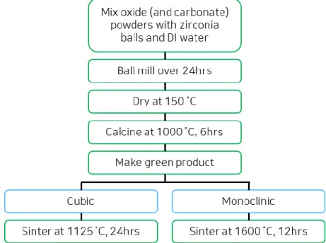
Bulk polycrystalline pellets for electrical measurements and targets for pulsed laser deposition were prepared via a series of ceramic processing steps listed in Fig. 3.1. In this study, traditional ceramic processing was used to produce composition and phase-controlled gadolinium-based oxides. The powders purchased from Alfa Aesar (Gd2O3 99.9 %, ZrO2 99.5 %, CeO2 99.5 %, SrCO3 99.99 %) and BeanTown Chemical (CaCO3 99.95 %) were used in this study. The pellets were made via successive ball milling, calcination, pressing, and sintering. Two different sintering conditions were applied to control phase. The relative density range of samples was 80%-85% for cubic phase and 85%-90% for monoclinic phase specimens. The density of cubic phase samples was difficult to improve upon due to the sintering temperature limit set by the phase transition temperature to the monoclinic phase. In general, higher density pellets can be obtained by sintering finer grained powders leading researches to harness the Pechini or co-precipitation method during the powder preparation step. We also attempted to follow this approach to improve the density of the cubic pellets, however, nm-sized powders did not help in
increasing density. Instead, nm-sized powders led to smaller grain sizes with increased numbers of grain boundaries leading to higher grain boundary contributions to the impedance spectra of the samples.
3.2. Thin Film Deposition
Thin film samples were prepared to correlate properties with the established defect model and observe the behavior of Gd2O3 – based MIM structures near room temperature. Pt was chosen for the metal layer due to its catalytic ability in exchanging oxygen and water and sapphire (C-plane, MTI Corp.) was chosen as the substrate due to its electrically insulating nature. Metal deposition on oxide substrates generally results in poor adhesion. To prevent this, Ti was used as an adhesion layer. The Gd2O3 – based
compositions were selected based on predictions of the established defect and transport models. Crossbar array MIM structures, as illustrated in Figure 3.2, were utilized to minimize scratching and pressure dependent problems associated with contacting probes directly to electrodes covering the active device regions.
Figure 3.2. (a) A schematic of sample with MIM structure. (b) photos of device structure after each preparation step.
3.2.1. Sputter Deposition
All the metallic components were deposited via DC magnetron sputtering (Kurt J. Lesker). Pt (ACI Alloys) and Ti (Kurt J. Lesker) with 4N purity were used as targets. The deposition of MIM structures required patterning. This study. Stainless-steel sputter masks, used to fabricate the structures, were ordered from PhotoEtch Technology. Before deposition, the sapphire substrates were immersed in
followed by Pt deposition, without breaking a vacuum. After deposition, the Gd2O3 – based oxide layer was deposited via PLD. Another mask was applied on top of the oxide layer, and the top Pt electrodes were deposited through them. In all cases, the metal deposition was conducted under the following conditions: 10-5 Torr base pressure, 4 mTorr working pressure, with ultrapure grade Ar (Airgas) atmosphere, and 50W DC power.
Figure 3.3. Thin film deposition techniques. (a) sputtering (b) pulsed laser deposition.
3.2.2. Pulsed Laser Deposition (PLD)
Pulsed laser deposition (PLD, Neocera Inc.) was chosen as the oxide deposition technique in this study due to the ease of producing various complex oxides. The targets were produced via ceramic processing as explained above. A substrate holder/mask was prepared by cutting Inconel 625 with a waterjet cutter (OMAX Corp.) to ensure that the bottom electrode area remained uncovered. After the sapphire substrates with bottom electrodes and the target were loaded into the chamber, the chamber was pumped down to below 5×10⁻⁶ Torr, then the chamber was filled with oxygen to 15 mTorr and the substrates heated to 500 ˚C. After 10 min, the source material was ablated via KrF excimer laser (248 nm wavelength) pulses generated by a COMPex Pro 205 laser (Coherent Inc.) for the oxide deposition. The energy per pulse was 300 mJ and the repetition rate was 1 Hz. Here, we targeted decreased thickness and temperature but there were short-circuiting issues with the thinner and rougher films. We initially attributed this to the PLD deposition mechanism (Volmer-Weber growth or island growth). It seems that the island-type nucleation and growth separated the film grown on the top of the bottom electrodes from the film grown directly on the substrates, resulting in a shorting between top and bottom electrodes following the sputtering process.
3.3. Physical Characterization
3.3.1. X-Ray Diffraction (XRD)
Due to polymorphism, a crucial criterion was to identify the phases of the specimens to be able to better relate properties to structure. For both pellet and thin film cases, X-ray diffraction (XRD) measurements were performed to identify the samples’ phase. The pellets and targets were characterized by a
PANalytical X'Pert PRO XRPD Diffractometer (Malvern Instruments) with an Open Eulerian Cradle sample stage. 2Θ scans with Bragg-Brentano geometry were taken over 20˚ to 60˚. The acquired spectra were analyzed using HighScore (Malvern Instruments) and reference profiles from ICCD.
Thin films were characterized by using SmartLab (Rigaku). Here again, the phase of the thin film was a key parameter. Besides, the thin film microstructure was regarded as important since there have been multiple reports about high proton conductivity via grain boundaries at lower temperature. To identify the phase and texture of the thin films, 2Θ – ω scans and rocking curve measurements were conducted under the plane beam focusing mode with Ge (220) monochromator. The 2Θ – ω scans were swept over 20˚ to 70˚ to distinguish multiple peaks near 30˚ by observing peaks near 65˚. The acquired spectra were analyzed as done in the powder diffraction studies.
3.3.2 Scanning Electron Microscopy (SEM)
Scanning electron microscopy (SEM) is a simple tool for observing surface morphology (microstructure) to a few nm ranges. This tool was used to observe grain size of pellets and powders or the microstructure of deposited film. In addition, this technique was useful to support proton conductivity trend near room temperature. During the investigation on the thin film samples, we observed various microstructure changes such as bubble formation, pinhole formation, etc, and these were turned out as a crucial feature to explain the MIM structure and the conductivity of oxide. The images were taken by Merlin
High-resolution SEM (Carl Zeiss AG)
3.3.3. Thermogravimetric Analysis (TGA)
measurement was unsuccessful since we ignored the effect of possible hydration that we learned later to be important in these materials.
Ultimately, the measurement was effectively used for making correlations between the materials’
hydration levels and their electrical conductivity near room temperature. At low enough temperatures, the proton conductivity in oxides tends to increase with decreasing temperature due to proton conduction at open pores or grain boundaries. To correlate hydration and conductivity, TGA measurements were performed under three different atmospheres (Wet N2, O2, and lab air) from 20 ˚C to 250 ˚C. The measurements were conducted utilizing a homemade TGA setup with temperature and atmosphere-controlled chamber.
3.4. Electrical Characterization
3.4.1. Electrochemical Impedance Spectroscopy (EIS)
Electrochemical impedance spectroscopy (EIS) is a very useful electrochemical method, especially when the electrical response is composed of multiple contributions. The EIS equipment reads the current response of a system under a small amplitude applied sinusoidal (AC) voltage over a wide range of frequencies. The complex impedance (Z) can be expressed as
𝑍 = |𝑍|𝑗𝜃⋯ (3.1)
where |𝑍| is the magnitude of the response, 𝑗 is the imaginary unit, and 𝜃 is the retardation of the response from the stimulus. For example, if an ac voltage bias V is applied through a resistor with resistance 𝑅, the current response I remains in phase with applied voltage, and 𝑍 = |𝑍| = 𝑅 = 𝑉/𝐼 where 𝑉 is applied voltage and 𝐼 is electrical current. Among the ways to express and analyze impedance, one intuitive way is plotting impedance in the complex plane (Nyquist plot). When one expresses equation 3.1 with real (𝑍′) and imaginary components (𝑍′′), the impedance can be expressed as
𝑍 = 𝑍′ + 𝑗𝑍′′ ⋯ (3.2)
Here, the magnitude of the real and imaginary parts can be expressed by using trigonometric functions and the magnitude of the impedance.
For analyzing the impedance spectra in terms of equivalent circuits, circuit components need to be expressed based in terms of the complex impedance. The real part of an impedance is an ideal resistor. The capacitor and the inductor are the components making the current response lag and lead by 𝜋
2,
respectively. Mathematically, the impedance of a resistor (𝑍𝑅), a capacitor (𝑍𝐶), and an inductor (𝑍𝐿), can be expressed as: 𝑍𝑅 = 𝑅 ⋯ (3.4) 𝑍𝐶 = 1 𝜔𝐶 𝑒 −𝑗𝜋 2 = 1 𝑗𝜔𝐶⋯ (3.5) 𝑍𝐿= 𝜔𝐿 𝑒𝑗 𝜋 2 = 𝑗𝜔𝐿 ⋯ (3.6)
where 𝜔 is the sweeping frequency in radians, 𝐶 is capacitance, and 𝐿 is inductance.
In solid oxides, many processes can be considered as parallel RC circuits. In this equivalent circuit, R represents transport/transfer of charge carriers and C represents polarization of the charges. When one imagines a simple system containing an oxide and an electrode, the significant electrochemical components come from the grains, grain boundaries, and electrodes (Figure 3.4). Oxides can be
considered as electrolytes, mixed electronic ionic conductors, or semiconductors. Grain boundaries create space charge regions adjacent to the grain due to the grain boundary potential that is generated at the core. These respectively can be understood as simple RC circuits. Electrode creates electric double layers at the interfaces, if the electrode exchanges ions, as in Figure 3.4, the electrode contribution can be understood as an RC circuit. If the electrode blocks ionic transfer, the electrode can be understood as a pure capacitor.
Figure 3.5. An example of the Nyquist plot from EIS of a solid with grain/grain boundary/electrode contributions. Reprinted from reference. [64] (Copyright by Annual Reviews)
Such equivalent RC circuits appear as semi-circles in the complex impedance plane. If one develops the impedance of a simple RC circuit from equation 3.4 and 3.5, the impedance (𝑍𝑅𝐶) can be expressed as
𝑍𝑅𝐶 = 𝑅
1 + 𝑗𝜔𝑅𝐶⋯ (3.7)
From equation 3.7, we can understand that semi-circles develop from right to left in Figure 3.4 as the frequency of the applied potential ranges from low to high frequency. Examining equation 3.7, we can easily determine that at the midpoint of the arc, (𝑅/2, −𝑅/2), the frequency is given by 𝜔𝑅𝐶 = 1 𝑅𝐶⁄ , the inverse of the well-known RC time constant, 𝜏𝑅𝐶 = 1 𝜔⁄ 𝑅𝐶. In general, the grain contribution is
characterized by the lowest RC time constant. Grain boundary and electrode contributions tend to have larger resistances and capacitances than those of the grain contribution owing to space charge effects and narrow double-layer widths. In most cases, the grain boundary follows the grain contribution at lower frequencies and with the electrode contribution coming at the lowest frequencies. However, if the
![Figure 1.3. Structure of the magneto-ionic device. Reprinted from reference. [15] (Copyright by Nature Research)](https://thumb-eu.123doks.com/thumbv2/123doknet/14672056.557043/19.918.277.644.483.860/figure-structure-magneto-reprinted-reference-copyright-nature-research.webp)
![Figure 1.4. Mechanism of magneto-electric effect. Reprinted from thesis of Bauer, U.. [31] (Copyright by Massachusetts Institute of Technology)](https://thumb-eu.123doks.com/thumbv2/123doknet/14672056.557043/22.918.236.682.139.444/figure-mechanism-electric-reprinted-copyright-massachusetts-institute-technology.webp)