A Comparator-Based Switched-Capacitor
Pipelined Analog-to-Digital Converter
by
John K. Fiorenza
B.S., University of Notre Dame (1999)
S.M., Massachusetts Institute of Technology (2002)
Submitted to the Department of Electrical Engineering and Computer
Science in partial fulfillment of the requirements for the degree of
Doctor of Philosophy in Electrical Engineering and Computer Science
at the
MASSACHUSETTS INSTITUTE OF TECHNOLOGY
June 2007
c
° Massachusetts Institute of Technology 2007. All rights reserved.
Signature of Author . . . .
Department of Electrical Engineering and Computer Science
March 14, 2007
Certified by . . . .
Hae-Seung Lee
Professor of Electrical Engineering
Thesis Supervisor
Certified by . . . .
Charles G. Sodini
Professor of Electrical Engineering
Thesis Supervisor
Accepted by . . . .
Arthur C. Smith
Chairman, Department Committee on Graduate Students
A Comparator-Based Switched-Capacitor Pipelined
Analog-to-Digital Converter
by
John K. Fiorenza
Submitted to the Department of Electrical Engineering and Computer Science on March 14, 2007, in partial fulfillment of the
requirements for the degree of
Doctor of Philosophy in Electrical Engineering and Computer Science
Abstract
A new comparator-based switched-capacitor(CBSC) technique is proposed that elim-inates the need for high gain op-amps in switched-capacitor circuits. The CBSC technique replaces the op-amp in switched-capacitor circuits with a comparator and a current source. Compared to op-amps, comparators suffer less from the negative effects of scaled CMOS. The technique is applicable to a broad class of sampled-data circuits including analog-to-digital converters, digital-to-analog converters, sample-and-holds, integrators and filters. As a proof of concept the technique is demon-strated in the design of a pipelined analog-to-digital converter. The prototype CBSC 1.5 b/stage pipelined ADC implemented in a 0.18 µm CMOS process operates at 7.9 MHz, achieves 8.6 effective bits of accuracy, and consumes 2.5 mW of power.
Sources of offset and nonlinearity are identified and analyzed. The analysis reveals the potential of the CBSC technique for lower power dissipation and provides design guidelines for energy efficient comparator-based switched-capacitor circuit design.
Thesis Supervisor: Hae-Seung Lee
Title: Professor of Electrical Engineering Thesis Supervisor: Charles G. Sodini Title: Professor of Electrical Engineering
Acknowledgments
Looking back at my time at MIT what I will remember most vividly, more than the time I spent working on research or the time spent studying for classes will be the time I spent with the people I met at MIT. Given that my time here has been large portion of my adult life, this is not surprising. This is also not surprising, given that a vast majority of what I learned here technical or otherwise was taught to me by someone I met along the way. All of these people deserve the credit for whatever I achieved here and for all that I take from this place.
I’d like to thank my advisors Professors Harry Lee and Charlie Sodini for all of their patience, help and guidance over the years. They have taught me a tremendous amount of technical knowledge and helped me to develop as an engineer. They have also through instruction and example taught me the right way to conduct one’s professional life. Finally they have entrusted me with some of their best ideas, and for this I am very grateful. Peter Holloway also deserves recognition for his contributions to my education and to the success of our project. His contributions, whether they were highly theoretical and abstract or highly practical and narrowly applied to our project, were instrumental in the success of our project. Professor James Roberge also was kind enough to add his contributions and perspective to the project by joining my committee and reading this thesis.
Todd Sepke shared a meeting with me for six years and a project with me for three years. He was always willing to work harder and to take less credit that he should. He also demonstrated a willingness to listen to my confused questions about circuits or my misguided proclamations about the world.
The members of the Lee and Sodini research groups made my time at MIT an invaluable and unforgettable experience. They both aided by technical education and made 38-265 a fun and open place to spend a number of years. The senior students patiently answered my questions and withstood my youthful ignorance. They include Dan McMahill, Don Hitko, Iliana Chen, Ginger Wang, Pablo Acosta Serafini, Kush Gulati, Aiman Shabra, Susan Luschas and Mark Peng. My contemporaries were willing to learn along with me, to share the joys and pains of grad school with me and to provide opportunities to escape from the occasional drudgeries of MIT. They include, my fellow Fall 2000 entrants, Todd, Anh Pham and Lunal Khoun, who shared the road of grad school most closely with me; Mark Spaeth, whose knowledge of Linux, CAD, circuits and electronics and whose sense of humor all contributed to my time spent in the office; my long time cubemates Andy Wang and Kevin Ryu, who have put up with all of my distractions over the years; my fellow long time Lee students and short time CBSC designers: Matt Guyton and Albert Chow; the shorter time Lee students: Andrew Chen, and Lane Brooks, the Sodini students: Farinaz Edalat, Albert Jerng, Khoa Nguyen, Johnna Powell and Ivan Nausieda; and the masters students: Nir Matalon, Jit Ken Tan, Matt Powell, Kartik Lamba, Jenny Lee and Albert Lin. During the last months of my time here a new group of students has joined the lab. They have added a new energy and enthusiasm to the room. The
new Sodini students include Yun Wu, David He, Ke Lu and Rahul Hariharan. The new Lee students: Jack Chu, Jeff Feng, Mariana Markova and Sungah Lee, have all recently joined the group to work on CBSC. I have been lucky to have the opportunity to discuss new ideas with them and to attempt to answer some of their questions.
My family has provided support and encouragement throughout my time at MIT and provided me with all the advantages needed to ease my path through life. I thank my mother Ann, my father Bob, who could have never imagined that two of his sons would spend nearly four times as long at MIT as he did, my brother Jim, who paved the way for me at MIT and made the task of completing the Ph.D. seem less daunting than it would have otherwise, my brother Paul, my sister Monica, my sister-in-laws Kim Tresch and Jen Fiorenza, my brother-in-law Greg McCormick and my nieces and nephews Matt, Nick, Kate and Sophia.
I have had the opportunity to make many friends among the grad students of MIT. They have added to the depth of my technical and personal experience at MIT. The members of the MTL have made the lab a fun place to work, have filled the field or rink for our intramural teams and have been willing to come together to constitute pretty strong pub quiz team. They include Andy Fan, Andy Ritenour, John Hennessy, Niamh Waldron, Denis Ward, Cait Ni Cleirigh, Nisha Checka, Luis Velasquez Garcia, Joyce Wu, Isaac Lauer, Fletch Freeman and Scott Meninger.
The members of TCC have helped to add balance to my life at MIT. They include Elizabeth Basha, Hayley Reynolds, Joe Laracy, Bridget Englebretson, Mihai Anton, Adam Nolte, Fr. Paul Reynolds and Fr. Richard Clancy.
My roommates have been good friends and have helped me out in numerous ways throughout my years here. Thanks to Will Kuhlman, Trent Yang, Andy Rakestraw, Mike Baffi, Sudeep Agarwala and Mike Stolfi.
My friends from Vermont have encouraged me to work hard with periodic prodding emails and have provided needed distractions from work by taking me out to Bosstones or Dropkick Murphys shows in Boston. Thanks go to my friends from kindergarten Ralph Bernardini, Julia Bernardini and Dave Deforge. Also thanks to all those who have joined our group in the last 25 years including Sage Bernardini, Amelia Gulkis, Nate Cross and Tessa Hunt. Thanks to Dan Buermann for joining Julia and I as Vermonters living in exile in Boston.
My professors and friends from Notre Dame helped to prepare me for the MIT experience. Thanks go to Professor Patrick Fay, Jackie Woo, Erin Neil, the ND EE class of 1999 and the Fisher Hall class of 1999, especially Matt Roder, Chris Backus, Brian Dougherty and Pat Noone.
My year at the Louverature Cleary School in Santo Haiti gave me a welcome break from school and gave me a broad view of the world to take with me to MIT. Thanks to Sean Bettinger-Lopez, Carries Bettinger-Lopez, Kate Kowalski, Patrick Moynihan, Gary Delice and the rest of the students and staff of LCS.
I would like to thank the staff of the MTL including Carolyn Collins, Rhonda Maynard, Kathy Pautenaud, Debb Hodges-Pabon and Marylin Pierce. All of whom worked to ease my path through the MIT administration.
The author was funded by the FCRP Focus Center for Circuit & System Solutions (C2S2), under contract 2003-CT-888, by DARPA under grant N66001-06-1-2046 and by the MIT Center for Integrated Circuits and Systems (CICS). The chip fabrication and packing for the prototype in this thesis were donated by National Semiconductor.
Contents
1 Introduction 15
1.1 Motivation . . . 15
1.2 Prior Work . . . 17
1.3 Thesis Organization . . . 18
2 Comparator Based Switched Capacitor Circuits 19 2.1 Comparator-Based Switched-Capacitor Circuits . . . 19
2.2 Comparator-Based Switched-Capacitor Charge Transfer . . . 22
2.3 Conclusion . . . 27
3 Traditional Pipelined ADC 28 3.1 Operation and Architecture . . . 28
3.2 Op-Amp Based Circuit Implementation . . . 29
4 CBSC Pipelined Design 34 4.1 CBSC Applications . . . 34
4.2 1.5 b/stage CBSC Pipelined ADC . . . 34
4.2.1 Threshold Detection Comparator . . . 35
4.2.2 Bit Decision Comparator . . . 36
4.2.3 Ramp Generation . . . 38
4.2.4 Clock Generation and Control . . . 41
4.2.5 Input Sampling . . . 46
5 Offset and Nonlinearity in CBSC Circuits 52
5.1 Sources of Offset and Nonlinearity in CBSC Circuits . . . 52
5.1.1 CBSC Error Sources . . . 53
5.1.2 CBSC Nonlinearity . . . 55
5.1.3 Other Sources of Nonlinearity and Offset . . . 63
5.2 Techniques to Increase Accuracy in CBSC Circuits . . . 64
5.2.1 Multiple Ramps . . . 64
5.2.2 Overshoot Correction . . . 64
5.3 Limitation of Linearity and Speed . . . 68
5.3.1 Linearity and Overshoot . . . 69
5.3.2 Linearity-Speed Trade Off . . . 70
5.4 Implementation Details . . . 89
5.4.1 Preset Time . . . 89
5.4.2 Excess Overshoot Requirement . . . 90
5.5 Design Procedure . . . 93
5.6 Conclusion . . . 93
6 Test System and Results 95 6.1 Introduction . . . 95
6.2 Test System . . . 95
6.2.1 Printed Circuit Board Layout . . . 96
6.2.2 Printed Circuit Board Circuits . . . 97
6.3 Results . . . 100
6.3.1 Measured Results . . . 100
6.3.2 Static Performance . . . 100
6.3.3 Dynamic Performance . . . 100
6.3.4 Figure of Merit . . . 103
7 Conclusions 108 7.1 Conclusions . . . 108 7.2 Thesis Contributions . . . 109 7.3 Future Work . . . 110
References 111
A Linearity Analysis Derivation 115
A.1 Two Phase CBSC Circuit . . . 115 A.2 Three Phase CBSC Circuit . . . 121
B Cascode Bias analysis 129
B.1 Sooch Cascode Bias Circuit . . . 129 B.2 Sooch Cascode Bias Circuit Using Series Triode Devices . . . 132
List of Figures
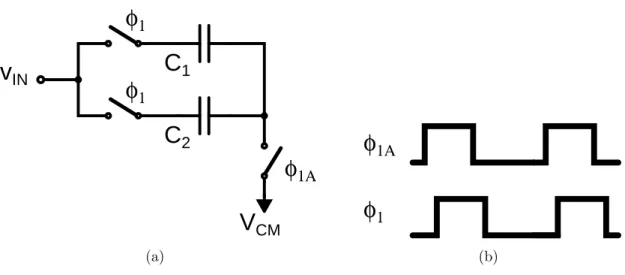
2-1 Bottom plate open-loop sampling (a) Sampling circuit. (b) Sampling clocks. φ1A defines sampling instant to minimize input dependent
charge injection. . . 20 2-2 Op-amp based switched-capacitor gain stage charge transfer phase.
(a) Switched-capacitor circuit (b) The output voltage exponentially settles to the final value. (c) The summing node voltage exponentially settles to the virtual ground condition. . . 20 2-3 Comparator-based switched-capacitor gain stage charge transfer phase.
(a) Switched-capacitor circuit with an idealized zero delay comparator. (b) The output voltage ramps to the final value. (c) The summing node voltage ramps to the virtual ground condition. . . 22 2-4 CBSC Clock Cycle: Preset (P ), Coarse Charge Transfer Phase (E1); it
has a variable duration depending on the input, Fine Charge Transfer Phase (E2); it has a variable end point depending on the input . . . 23
2-5 Preset phase (P ). (a) Switch P closes. (b) vOgrounded and vX brought
below VCM . . . 23
2-6 Coarse charge transfer phase (E1). (a) Current source I1 charges
out-put. (b) vO and vX ramp and overshoot their ideal values. . . 24
2-7 Fine charge transfer phase (E2). (a) Current source I2 discharges
2-8 Overshoot cancellation. (a) CBSC stage with overshoot cancellation. (b) vX node voltage during the charge transfer phase without overshoot
correction. The large overshoot during the coarse phase prevents the charge transfer operation from finishing in allowed time. (c) CBSC
stage with overshoot cancellation. . . 26
3-1 Pipeline ADC . . . 29
3-2 Pipeline ADC stage . . . 29
3-3 Traditional op-amp based 1 b/stage Pipelined ADC stage . . . 30
3-4 Residue plot of a single stage of a 1 b/stage Pipelined ADC. . . 31
3-5 Traditional op-amp based 1.5 b/stage Pipelined ADC stage . . . 32
3-6 Residue plot of a single stage of a 1.5 b/stage Pipelined ADC. . . 33
4-1 First two stages of the prototype Pipelined ADC. . . 35
4-2 Diagram of the Threshold Detection Comparator . . . 36
4-3 The Threshold Detection Comparator Schematic . . . 37
4-4 Bit Decision Comparator Schematic . . . 37
4-5 Coarse Current Source. . . 38
4-6 Fine Current Source. . . 42
4-7 (a) CBSC state machine. (b) CBSC control signals. . . 43
4-8 Level detection comparator reference switching. . . 44
4-9 Nonoverlaped Clock Generation Circuit. . . 44
4-10 Clock Generation Circuit. . . 45
4-11 Input sampling circuits. (a) Input sampling circuit of the first stage. (b) Input sampling circuit of the second through twelfth stages. . . . 46
4-12 Die photograph. 0.18 µm CMOS process. Pipeline Area: 1.2 mm2. . . 49
4-13 Layout of one stage of the prototype Pipelined ADC . . . 50
4-14 Floor plan of one stage of the prototype Pipelined ADC . . . 51
5-1 Switch resistance errors: vRS and vRI create offset, vRL causes nonlin-earity . . . 54
5-2 Output voltage slope variation : Depending on the output voltage the slope will be different. The difference in the slopes causes the output to overshoot different amounts during the delay time. The output variation is shown for a comparator with a fixed delay. . . 57 5-3 Overshoot cancellation. (a) CBSC stage with overshoot cancellation.
(b) vX node voltage during the charge transfer phase without overshoot
correction. The large overshoot during the coarse phase prevents the charge transfer operation from finishing in allowed time. (c) CBSC stage with overshoot cancellation. . . 66 5-4 The maximum overshoot correction is determined by the ramp
linear-ity. The output must overshoot for all input voltages. The smallest overshoot is completely canceled and the largest residual overshoot depends on the ramp nonlinearity and the value of the original uncor-rected overshoot, VOV. . . 67
5-5 The maximum possible overshoot correction (VCORM AX) is determined
by the minimum output voltage. . . 68 5-6 Noise bandwidth comparison. (a) Op-amp time constant (τo). (b)
Com-parator delay (td≈ ti). . . 73
5-7 Two-phase circuit output voltage: The minimum charge transfer time is achieved when t1=t2. . . 76
5-8 Three-phase circuit output voltage . . . 78 5-9 Number of comparator delays or time constants vs linearity in terms
of Bits. The values used were the same as those used in the prototype. The full scale voltage VF S is 1.0 V. The minimum input voltage VM IN
is 0.4 V. The maximum input voltage VM AX is 1.4 V. . . 79
5-10 VOU T for a two ramp system. As the required bit resolutions declines,
VOV 2and VOV 1can increase and the required number of delays (α1) can
decrease. . . 80 5-11 Two-phase number of comparator delay vs Bits . . . 81
5-12 Fraction (α) of the half clock cycle, T
2 occupied by the final phase
com-parator delay td2 vs. Linearity with an integrating final comparator.
The linearity of each circuit is required to be 1
2LSB referred to the
input. The sampling frequency is 10 MHz and first and second fixed ramp delays are each 1% of the half clock cycle (td1 = 500 ps). . . 85
5-13 Transconductance vs. Linearity with an integrating final comparator: The linearity of each circuit is required to be 1
2 LSB at the input. The
sampling frequency is 10 MHz and first and second fixed ramp delays are each 500 ps. . . 86 5-14 Transconductance vs. Linearity and Noise with an integrating final
comparator: The linearity and mean squared noise of each circuit is required to be 1
2LSB at the input. The sampling frequency is 10 MHz
and first and second fixed ramp delays are each 500 ps. . . 87 5-15 A CBSC stage with an integrating final comparator: The linearity and
mean squared noise of each circuit is required to be 1
2LSB at the input.
The sampling frequency is 10 MHz. The first and second fixed ramp delays are each 5 ns. (a) Transconductance vs. Linearity and Noise (b) Fraction (α) of the half clock cycle occupied by the final phase comparator delay vs. Linearity. . . 88 5-16 (a) Comparator integrating preamplifier schematic (b) Comparator
in-tegrating preamplifier output. The output reaches and stays at the clamped state before flipping. Memory of the coarse phase is erased. (c) Comparator integrating preamplifier output that does not reach the clamped state . . . 91
5-17 Switch voltage drop transient. (a) The switch voltage drop ∆ vOǫ rappears
at the output during the transition from the coarse phase to the fine phase. A transient occurs as vO settles to a constant ramp. (b) The
output current switches direction during the transition from the coarse phase to the fine phase. The coarse current source turns off and the
fine current turns off during the transition. . . 92
6-1 Test setup. The component descriptions above the blocks correspond to static testing while the component descriptions below the blocks correspond to dynamic testing. . . 96
6-2 Voltage bias circuit. . . 98
6-3 Current bias circuit for on chip PMOS current mirrors. . . 99
6-4 Current bias circuit for on chip NMOS current mirrors. . . 99
6-5 ADC INL and DNL for 7.9 MHz sampling frequency. (a) DNL. (b) INL.101 6-6 Output FFT for 7.86MHz clock and 3.8MHz input. . . 102
6-7 SNDR and SFDR versus input frequency. . . 103
6-8 Simulated ADC INL: the INL is less than +0.2/-0.4 LSB10 . . . 105
6-9 Simulated ADC INL using updated NMOS models: the INL is +0.8/-0.2 LSB10 . . . 106
A-1 Two-phase circuit output voltage: The minimum charge transfer time is achieved when t1=t2. . . 116
A-2 Three-phase circuit output voltage . . . 121
B-1 Coarse current source with Sooch Bias. . . 130
List of Tables
4.1 Coarse Current Source Transistor sizes . . . 39
4.2 Fine Current Source Transistor sizes . . . 42
4.3 Sampling circuit transistor sizes . . . 46
Chapter 1
Introduction
The needs of large digital systems have driven the development of modern scaled CMOS processes. Process advances such as lower power supplies and shorter gate lengths which lead to lower power consuming, faster digital circuits can also lead to higher power consuming, lower performance analog circuits. Although the higher fTs
of scaled devices can be used to increase analog performance, other process char-acteristics such as reduced transistor output resistance and lower supply voltage make the design of op-amps, a fundamental analog building block, more challeng-ing. Traditional analog design techniques require op-amps with very high gain to achieve accurate results. The objective of this work is to develop a comparator-based switched-capacitor technique that removes the need for op-amps in switched-capacitor circuits.
1.1
Motivation
The persistent advance of CMOS process technology which has enabled unprecedented performance advancement of digital integrated circuits has also created many new challenges in the design of analog integrated circuits. Analog designers have been able to overcome the challenges of modern CMOS technology in order to take advantage of its inherent advancement. As CMOS continues to scale this will become more and
more difficult.
One of the most important design challenges posed by CMOS scaling is the design of high gain operation amplifiers (op-amps). Op-amps are essential analog building blocks. They often limit the performance integrated systems. Often the gain of the op-amp will limit the accuracy of the analog system and the bandwidth of the op-amp will limit the speed of the system. One specific example is the pipelined analog-to-digital converter. The gain of op-amps contained in the input sample-and-hold as well as the pipeline stages will directly limit its accuracy.
Two aspects of CMOS scaling are increasing the difficulty of designing high gain op-amps: smaller gate length and reduced supply voltage.
The ever shrinking gate length of modern CMOS devices is the heart of CMOS scaling. Smaller transistors enable faster smaller digital circuits, but also provide lower output resistance (ro). Since the gm× ro product of a transistor fundamentally
limits the gain of any amplifier, scaled devices produce lower gain op-amps. This effect could traditionally be negated by using longer than minimum length devices in a design. Intrinsic speed (fT) would be sacrificed for higher intrinsic gain. The
output resistance of of a modern digital devices [1] does not increase significantly with increasing length. This effect is due to the pocket implants that are used to maintain gate control of deeply scaled devices. Unfortunately, the output resistance of such devices is primarily determined by the modulation of the energy barrier created by the pocket implant [2–4] rather than by channel length modulation. Increasing the gate length does not significantly effect this mechanism, therefore increasing gate length does not significantly improve output resistance.
Reduced supply voltages are both a feature and requirement of scaling. Using a lower supply voltage enables lower power consumption in digital circuits, but it is also a requirement of using scaled devices. In order to maintain gate control over very small devices it is required that one uses a very thin gate oxide. A low supply voltage must be used in order not to damage this oxide or cause break down in the very short channel. Unfortunately in analog circuits a lower supply voltage usually
leads to higher power dissipation for a similarly performing circuit. A lower supply voltage limits the output swing and consequently causes the signal to noise ratio to decrease. In order to maintain the same signal to noise ratio capacitor sizes must be increased to reduce kT
C noise. The power consumption of the circuit must be increased
to drive the larger capacitors at the same speed as the original circuit.
In order to achieve reasonable gain in an amplifier designed in a scaled technology it is often necessary to cascode transistors. The cascoded topology further reduces the already limited output swing.
To address the challenges of scaled CMOS analog circuit design, a new class of comparator-based switched-capacitor circuit topologies is proposed [5, 6], that does not require op-amps in the signal path. The combination of a comparator and a cur-rent source replaces the op-amp. Most techniques and architectures used in traditional op-amp based switched-capacitor circuits [7] can also be used in comparator-based switched-capacitor circuits.
1.2
Prior Work
Many different approaches have been taken to address the challenge of designing high gain amps in scaled CMOS technology. One alternative to a cascoded op-amp is to cascade several lower gain stages to create an overall high gain op-op-amp. Stabilizing such an amplifier in feedback becomes problematic. Techniques used to stabilize the amplifier, such as nested Miller compensation [8], require an increased power consumption to maintain the same speed of operation.
Different techniques have been developed to avoid or to compensate for the ef-fects of low op-amp gain. One approach [9] uses a charge coupled device process to avoid the limitation of scaled CMOS. Dynamic amplifiers [10, 11] have been used to avoid explicit operational amplifiers, however, as dynamic amplifiers turn off, their input transistors enter weak inversion causing their outputs to settle very slowly. For low precision applications, parametric amplifiers [12] are another alternative. More
recently, digital calibration has been used to compensate for the poor performance of both low-gain op-amps [13] and open loop amplifiers [14]. Also finite gain com-pensation techniques have been developed [15, 16] which alter the traditional switch capacitor switching scheme to boost the effective gain of an op-amp.
Analog circuits have been designed in the past using comparators and current sources or voltage ramps. Examples include the dual slope ADC, a time based ADC [17] and a RipSaw ADC [18]. These techniques differ from the proposed technique in that they are specific methods for quantizing signals and are therefore only applicable to ADCs. Comparators have been used in a similar manner to the way they are used in the proposed technique for a low noise reset in imagers [19] and to produce sample-and-hold circuits using discrete components [20, 21].
1.3
Thesis Organization
Chapter 2 provides an introduction to the comparator-based switched-capacitor nique. This chapter explains the basic principle of operation and compares the tech-nique to the standard op-amp based switched-capacitor techtech-nique.
Chapter 3 reviews the operation of the pipeline ADC architecture. This describes the 1 b/stage and 1.5 b/stage ADC’s and discusses the effect of non-idealities on pipeline ADC performance.
Chapter 4 presents the details of the CBSC prototype 1.5 b/stage pipeline ADC. It outlines the overall design of the ADC as well as discussing the design of selected circuit blocks.
Chapter 5 examines the sources of offset and nonlinearity in CBSC designs and analyzes their effect on circuit performance.
Chapter 6 describes the overall test system including the PCB test board and presents the simulated and measured results of the prototype.
Finally, Chapter 7 summarizes the contributions of this thesis and suggests areas for future work.
Chapter 2
Comparator Based Switched
Capacitor Circuits
2.1
Comparator-Based Switched-Capacitor Circuits
The operation of op-amp based and comparator-based switched-capacitor gain stages are very similar. The fundamental difference is that while the op-amp forces the virtual ground condition for the entire charge transfer phase, the comparator detects the virtual ground condition and triggers sampling.
Traditional Op-amp Based Switched-Capacitor Gain Stage
An op-amp based switched-capacitor gain stage operates on a two phase cycle: a sampling phase and a charge transfer phase. During the sampling phase φ1, the input
voltage is sampled onto both C1 and C2 using the open-loop sampling circuit shown
in Fig. 2-1. The falling edge of the clock φ1A defines the sampling instant in order to
minimize signal dependent charge injection [22, 23].
For the charge transfer phase, the capacitors are reconfigured as shown in Fig. 2-2. The op-amp forces a virtual ground condition at the summing node, which transfers all the charge that was originally sampled on C2 onto C1. During the charge transfer,
v
INC
1C
2φ
1Αφ
1φ
1V
CM (a)φ
1Αφ
1 (b)Figure 2-1: Bottom plate open-loop sampling (a) Sampling circuit. (b) Sampling clocks. φ1A defines sampling instant to minimize input dependent charge injection.
V
CMV
CMV
CMC
2C
1C
Lv
Xv
O+
-+ − (a)v
O [n]v
Ot
(b)v
Xv
XoV
CMt
(c)Figure 2-2: Op-amp based switched-capacitor gain stage charge transfer phase. (a) Switched-capacitor circuit (b) The output voltage exponentially settles to the final value. (c) The summing node voltage exponentially settles to the virtual ground condition.
to their steady-state values as shown in Fig. 2-2. The time-constant of the closed loop system determines the settling speed. In the simplified one-pole system shown in Fig. 2-2 a single time constant determines the settling speed. In a more realistic multi-pole system the time constant of the decay of the output voltage envelope determines the settling speed. In either case, after a number of time constants the output voltage settles sufficiently and it is sampled onto the load capacitance CL.
The relationship between the input and the output samples is given by:
vO[n] =
µ C1+ C2
C1
vIN[n − 12]. (2.1)
During the charge transfer phase, the accuracy of the output voltage is directly related to the accuracy of the virtual ground condition. The op-amp tries to force the virtual ground in a continuous-time manner. However, the only time an accurate virtual ground is necessary in switched-capacitor circuits is at the sampling instant. Therefore, it should be possible to detect the virtual ground condition with a com-parator rather than force it with an op-amp. Also, the former should be more energy efficient than the latter.
Comparator-Based Switched-Capacitor Gain Stage
A comparator-based switched-capacitor gain stage operates on a similar two phase cycle as an op-amp based switched-capacitor gain stage. The sampling phase φ1 of
a comparator-based circuit is identical to the sampling phase of the op-amp based circuit (Fig. 2-1).
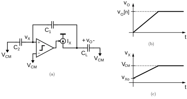
The charge transfer phase of a comparator-based switched-capacitor gain stage is shown in Fig. 2-3. The op-amp has been replaced with a threshold-detection comparator and a current source IX. During a short preset phase, not shown in
Fig. 2-3, vOis shorted to ground thereby presetting vX below VCM. Then, the current
source IX turns on, charges up the capacitor network consisting of C1, C2, and CL,
V
CMV
CMV
CMC
2C
1C
LI
Xv
Xv
O+
-+ − (a)v
Ov
O[n]t
(b)V
CMv
Xov
Xt
(c)Figure 2-3: Comparator-based switched-capacitor gain stage charge transfer phase. (a) Switched-capacitor circuit with an idealized zero delay comparator. (b) The output voltage ramps to the final value. (c) The summing node voltage ramps to the virtual ground condition.
to ramp until the comparator detects the virtual ground condition (vX=VCM), and
turns off the current source. In this way, the comparator determines the sampling instant. At the sampling instant, the same virtual ground condition has been obtained as in the op-amp based circuit. All the charge from C2 has transfered to C1, and the
same output voltage is sampled on CL.
2.2
Comparator-Based Switched-Capacitor Charge
Transfer
This section describes the comparator-based switched-capacitor charge transfer in greater detail. To achieve high accuracy and linearity the charge transfer phase is divided into three sub-phases: a preset phase (P ), a coarse charge transfer phase (E1), and a fine charge transfer phase (E2). The timing for a complete clock cycle
φ
2P E
1
E
2
: Charge Transfer
φ
1: Sample
Figure 2-4: CBSC Clock Cycle: Preset (P ), Coarse Charge Transfer Phase (E1); it
has a variable duration depending on the input, Fine Charge Transfer Phase (E2); it
has a variable end point depending on the input
V
CMV
CMV
CMC
2C
1C
Lv
Xv
O+
-S
P
+ − (a) φ2 S VCM vXo vO t vO[n] t vX P E1 E2 -VCM (b)Figure 2-5: Preset phase (P ). (a) Switch P closes. (b) vO grounded and vX brought
below VCM
E2 in order to minimize the sensitivity of the circuit to nonlinearity and to maximize
the accuracy of the circuit. The comparator decision time is allowed to take up most of E2 so that the noise bandwidth of the comparator can be minimized.
A short preset phase (P ), shown in Fig. 2-5, is used to ensure that vX starts below
the virtual ground condition. After sampling completes at the end of phase φ1, the
voltage vX is equal to VCM. During the preset, VCM is connected to C2, and the output
of the stage is connected to the lowest system voltage. This causes vX to step low and
results in VXo being less than VCM over the range of input voltages. The sampling
V
CMV
CMV
CMC
2C
1C
LI
1v
Xv
O+
-I
2E
1S
E
2 + − (a) φ2 S VCM vXo vO t vO[n] t vX P E1 E2 -VCM (b)Figure 2-6: Coarse charge transfer phase (E1). (a) Current source I1 charges output.
(b) vO and vX ramp and overshoot their ideal values.
The coarse charge transfer phase (E1), shown in Fig. 2-6, is used to get a fast,
rough estimate of the output voltage and virtual ground condition. The finite delay of the comparator and the high output ramp rate results in an overshoot of the correct value. When the comparator makes its decision, the current source I1 is turned off.
The fine transfer phase (E2), shown in Fig. 2-7, is used to get a more accurate
measurement of the virtual ground condition and consequently a more accurate value for the output voltage. The fine phase current I2 is much less than the coarse phase
current I1 and of opposite sign. This allows the comparator to have a long delay
without causing a large final overshoot.
When the comparator detects the second threshold crossing, the sampling switch S is opened. This defines the sampling instant and locks the sample charge on the load capacitance CL. The I2 current source is turned off slightly after the sampling
switch opens, but the extra current it sinks does not disturb the sampled charge because it only discharges the parasitic capacitance at the output node.
du-V
CMV
CMV
CMC
2C
1C
LI
1v
Xv
O+
-I
2E
1S
E
2 + − (a) φ2 S VCM vXo vO t vO[n] t vX P E1 E2 -VCM (b)Figure 2-7: Fine charge transfer phase (E2). (a) Current source I2 discharges output.
(b) vO and vX ramp to their final values.
ration of the coarse charge transfer phase E1 depends on the preset value vXo, which
depends on the input signal. The charge transfer is self-timed, but for correct opera-tion, the total charge transfer must be complete before the end of the time allocated for charge transfer. As shown in Fig. 2-7, the falling edge of φ2 represents the end of
the allocated charge transfer time.
During the coarse charge transfer phase, a large current is used to charge the out-put capacitance thereby creating a potentially large offset and nonlinearity. The large overshoot slows the operation of the circuit because the fine phase current requires a long time to discharge the output and recover from the coarse phase overshoot. In order to minimize this recovery time, a portion of the overshoot is canceled. One way to do this is to change the reference voltage of the level detection comparator from VCM to a lower voltage VOC. This operation is shown in Fig. 2-8, and is also discussed
in detail in Section 5.2.2. VOC is a reference voltage that is the same for all possible
output voltages. It is set to cancel as much of the overshoot as possible while still allowing the output to overshoot for all output voltages. If the overshoot is canceled
V
CM
V
CM
V
CM
C
2
C
1
C
L
I
1
v
X
v
O
+
-I
2
E
1
S
E
2
V
OC
E
1
E
2
+
−
(a)V
CMv
Xot
v
XV
OCt
d1v
OV1 (b)V
CMv
Xot
v
XV
OCt
d1t
d2v
OV1v
OV2 (c)Figure 2-8: Overshoot cancellation. (a) CBSC stage with overshoot cancellation. (b) vX node voltage during the charge transfer phase without overshoot correction.
The large overshoot during the coarse phase prevents the charge transfer operation from finishing in allowed time. (c) CBSC stage with overshoot cancellation.
too aggressively the output voltage will not overshoot for an output value and the circuit will not operate correctly.
2.3
Conclusion
The CBSC technique shares many similarities with traditional op-amp based switched capacitor circuits. The two techniques share the same two phase clock cycle and the same sampling phase. The charge transfer phase represents the difference between the two. During the charge transfer phase op-amp based circuits use the op-amp to continuously force a virtual ground while CBSC circuits use a comparator to sense a virtual ground condition.
Chapter 3
Traditional Pipelined ADC
Pipeline ADCs are high performing and versatile modern data converters. They are used in many applications including wireless systems, wireline systems, medical elec-tronics, still and video cameras and electronic test equipment. Commercial pipelined ADCs provide resolutions between 8 b and 16 b and have sampling rates between 1 MS/s and 250 MS/s [24–26]. This chapter provides a brief overview of pipelined ADCs and describes the traditional op-amp based pipelined ADC [27].
3.1
Operation and Architecture
Figure 3-1 shows the ADC architecture. The ADC consists of a number of stages (M). Each stage resolves n bits and produces a residue to pass on to the next stage. The ADC operates in a pipelined manner so that each stage is always either resolving bits and producing a residue or sampling the residue of the previous stage. The bits of all of the stages enter the shift register to be time aligned. The shift register outputs the total number of time aligned bits, nM .
Figure 3-2 shows the composition of a single stage. It consists of an n-bit ADC, an n-bit DAC and a amplifier and subtraction circuit. The ADC resolves the bits. The DAC and subtraction circuit subtract the analog representation of the resolved bits from the input signal. This value is then multiplied by 2nto produce the residue
v
INStage
1
v
RES1D(1)
nv
RES2Stage
2
nStage
M
nShift Register Buffers
D
OUTnM
D(2)
D(M)
Figure 3-1: Pipeline ADC
v
INADC
n
2
nv
RESiDAC
n
nD(i)
+
-Figure 3-2: Pipeline ADC stage
voltage.
For the case of a 1 b/stage Pipelined ADC each stage first determines whether an input is above or below the mid value of the input range (VCM) and then takes the
portion of the input range that the input is in and amplifies it and shifts it so that this residue takes up the entire input range of the next stage.
3.2
Op-Amp Based Circuit Implementation
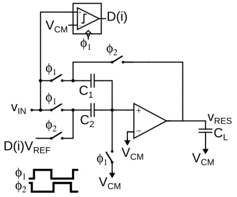
Traditional Pipelined ADCs employ op-amps to provide the amplification and sub-traction needed in a stage. The schematic of a stage of a 1 b/stage Pipelined ADC is shown in Figure 3-3.
This schematic is very similar to the op amp based gain-of-two stage discussed in chapter 2. A comparator has been added to resolve a bit and reference voltages are
− +
C
2C
1V
CMV
CMv
IND(i)V
REFφ
1φ
1φ
2φ
1V
CMD(i)
φ
1φ
1φ
2 + −φ
2V
CMC
Lv
RESFigure 3-3: Traditional op-amp based 1 b/stage Pipelined ADC stage
connected to C2. The stage produces the residue voltage,
vRES = C2+ C1 C1 • v IN− D(i) • C2 C1 • V REF. (3.1)
Ideally C1 = C2 and the residue is
vRES = 2 • vIN− D(i) • VREF. (3.2)
where
D(i) • VREF = VM IN vIN < VCM (3.3)
D(i) • VREF = VM AX vIN > VCM (3.4)
and the digital output bit is 1 for vIN > VCM and 0 for vIN < VCM.
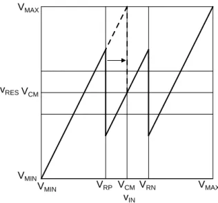
The plot of this residue is the solid line in Figure 3-4. Notice that in a 1 b/stage ADC any offset in the comparator will cause the residue voltage to exceed the
maxi-vRESVCM VCM VMIN VMIN VMAX VMAX
Figure 3-4: Residue plot of a single stage of a 1 b/stage Pipelined ADC.
mum voltage of the ADC, VM AX. This effect is shown by the dashed line. The offset
causes the residue voltage to exceed the input range of the succeeding stage. The portion of the residue that exceeds the input range is not processed by the rest of the pipeline. This effect causes gross nonlinearity in the ADC transfer characteristic and missing decision levels.
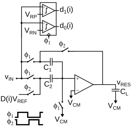
In order to avoid errors due to comparator offset, digital error correction [27] is usually used in the ADC design. One version of digital error correction is the 1.5 b/stage scheme [28–30]. An op-amp based implementation of the 1.5 b/stage ADC is shown in Figure 3-5. A second comparator is added to the 1 b/stage ADC as well as a third reference level. The reference levels are now
D(i) • VREF = VM IN vIN < VRN (3.5)
D(i) • VREF = VCM vIN > VRN& vIN < VRP (3.6)
D(i) • VREF = VM AX vIN > VRP. (3.7)
The bit decision is resolved to be 1 if vIN > VRP, 0 if vIN < VRP, and if vIN is between
− +
C
2C
1V
CMV
CMv
IND(i)V
REFφ
1φ
1φ
2φ
1V
RNd
0(i)
φ
1φ
1φ
2V
RP −d
1(i)
+ + −φ
2V
CMC
Lv
RESFigure 3-5: Traditional op-amp based 1.5 b/stage Pipelined ADC stage
later stage. The 1.5 b/stage residue plot in figure 3-6 shows that a small comparator offset will not cause the residue voltage to exceed the input range of the succeeding stage. To allow the maximum correction range for comparator offset VRN is set to
3
8VF S + VM IN and VRP is set to 5
8VF S+ VM IN where VF S = VM AX − VM IN. These
comparator reference levels allow each comparator to have offsets of ±1 8VF S.
The low intrinsic transistor gain in scaled technologies, described in Chapter 1, causes INL in Pipelined ADCs. Low gain transistors produce low gain op-amps which in turn produce stage gain error. Linear gain errors can be removed using well known calibration techniques [31]. Nonlinear gain errors can only be removed through statistical calibration using a large number of input samples [14]. Chapter 4 describes the application of the CBSC technique to a 1.5 b/stage ADC to address the effects of low op-amp gain on the performance of switched capacitor circuits.
vIN vRESVCM VCM VRP VRN VMIN VMIN VMAX VMAX
Chapter 4
CBSC Pipelined Design
4.1
CBSC Applications
The CBSC design method applies not only to the gain stage used in the description of the technique but to switched-capacitor circuits in general. The technique applies to a broad range of switched-capacitor circuits including, filters, integrators in sigma-delta converters, switched capacitor DACs, and switched-capacitor ADCs.
4.2
1.5 b/stage CBSC Pipelined ADC
As a proof of concept the CBSC method was applied to a 1.5 b/stage Pipelined ADC. A simplified schematic of the first two stages of the pipeline is shown in Figure 4-1. For the prototype, a single-ended circuit design was used as is shown in the schematic. The prototype consists of 13 identical stages. The first 12 stages resolved bits. The 13th stage is only present to provide a load for the 12th stage. The bit decisions of the 13th stage are not recorded. The later stages were left unscaled in order to simplify the design. They could be scaled to reduce the ADCs power consumption. Unlike a traditional 1.5 b/stage ADC the final stage does not produce a whole number of bits such as 1 or 2 bits, but rather ouputs three decisions. This could easily be changed by wiring the comparator references for the 12th stage to VCM rather than VRN and
− +
C
1bC
1aV
CMV
CMV
inD(0)V
REFφ
1φ
1φ
2φ
1I
1C
2bC
2aV
CMV
CMφ
2φ
2Stage 0
Stage 1
V
RNd
0(0)
φ
1φ
1φ
2I
2V
RP −d
1(0)
+ − +V
RNd
0(1)
V
RP −d
1(1)
+E
1E
2S
D(1)V
REFφ
1S
+ − + −Figure 4-1: First two stages of the prototype Pipelined ADC.
VRP and eliminating the 13th stage.
4.2.1
Threshold Detection Comparator
A critical circuit in the CBSC method is the virtual ground detection comparator. Unlike a traditional clocked comparator that compares voltages at a specific point in time the virtual ground detection comparator must detect the time a voltage ramp crosses the virtual ground condition and must then open the output sampling switch. Comparators can achieve high gain by cascading several gain stages. Because the comparator is only used in an open-loop configuration, there are no associated stability issues with this approach. A high level schematic of the comparator used in the prototype is shown in Figure 4-2. The first stage of the comparator determines the noise accuracy of the virtual ground detection. This band-limiting stage is followed by a series of 3 wide-band amplifying stages that drive a level converter to create the complementary logic signals used to control the current source and sampling switch
G
mV
CMV
xQ
Q
+
−
−
+
+
−
−
+
A
1+
−
−
+
A
2+
−
−
+
A
3+
−
−
+
A
4Figure 4-2: Diagram of the Threshold Detection Comparator
logic circuits.
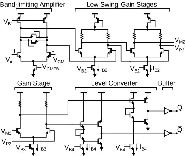
A more detailed schematic of the comparator is shown in Figure 4-3. The first stage is the actively loaded band-limiting stage. The stage’s common-mode feedback circuit is not shown in the figure. The output is clamped by two back-to-back MOS diodes for faster recovery of the comparator. Also, it is the total parasitic capaci-tance at the output of this first stage analog with its transconduccapaci-tance that sets the bandwidth. The band-limiting amplifier is followed by 2 low-swing, wide-bandwidth gain stages which drive the final gain stage. The final stage drives a pair of level converters whose outputs are buffered with standard CMOS inverters. For greater detail about the threshold detection comparator see [32].
4.2.2
Bit Decision Comparator
The bit decision comparators are dynamic clocked comparators. A schematic of the comparator is shown in Figure 4-4. At the falling edge of φ1 the input series switches
are opened. This samples the input and reference voltages on to the inputs of the cross coupled inverters. Just after the falling edge of φ1, φL rises and connects the
header switches, MP A and MP B, and footer switches, MN. This triggers the positive
feedback and causes the comparator to resolve a bit.
The inputs to the comparator are not high impedance nodes. This allows for the possibility that the comparator can draw extra current through its inputs during some portion of its input range. It has two independent header switches, MP A and
MP B, rather than a single switch seen in a traditional comparator in order to prevent
Band-limiting Amplifier
Low Swing
Level Converter
Buffer
Gain Stages
V
CMFBI
B2I
B2I
B3Q
V
B4V
B1Q
V
B4V
B3V
B2V
B2I
B4I
B4+
-V
xV
CMV
M2V
P2V
M2V
P2Gain Stage
Figure 4-3: The Threshold Detection Comparator Schematic
V
inV
REFφ
Lφ
1φ
1Q
Q
φ
LM
PAM
PBM
NM
1M
2M
3M
4E1 E1 VE1 VB1 NS PS I1 P1 P2 (a) P+E1D P+E1 VB I1 P1 W/L P2 P3 W3/L3=1/10W/L P4 P5D P6 N1 NS PS I1/10 W/L W3/L3 W3/L3 W3/L3 P5C P5B P5A W3/L3 W3/L3 W3/L3 (b)
Figure 4-5: Coarse Current Source.
4.2.3
Ramp Generation
Another important part of the implementation is the ramp generation. The prototype uses two switched current sources to produce the output voltage ramps.
The coarse charge transfer phase current source I1was implemented with a cascode
current source, and is switched on and off by controlling the gate voltage of the cascode device P2 as shown in Figure 4-5(a). During the coarse charge transfer phase E1 the
gate of the cascode transistor P2 is connected to the bias voltage VB1. After this
phase the gate of the cascode transistor P2 is disconnected from VB1 and connected
to the power supply. This action shuts the current source off.
The coarse current source for each stage has its own cascode bias circuit. This was done so the noise created by turning the current source off in one stage would not disrupt the bias voltage line and couple to the current sources in the other stages. A detailed view of the current source and bias circuit appears in Figure 4-5(b). The bias circuit is based on the Sooch mirror [33, 34]. Using this mirror reduces power consumption because it requires only one leg for biasing rather than the two legs required by the standard wide swing cascode bias [35–37]. Also the bias leg is scaled down by 10× to further reduce the power consumption of the circuit. Transistors P3
P1 24.8 µm/0.5 µm P2 24.8 µm/0.5 µm P3 2.48 µm/0.5 µm P4 2.48 µm/0.5 µm P5A-P5D 2.48 µm/0.5 µm P6 2.48 µm/0.5 µm PS 1 µm/0.18 µm N1 6 µm/1.5 µm NS 1 µm/0.18 µm I1 70 µA
Table 4.1: Coarse Current Source Transistor sizes
and P4 operate as they do in the wide swing cascode mirror. The gate of P3 is set
at VT + ∆ V below VDD because P3 is diode connected. Transistor P4 ensures that
P3 has ∆ V drop across it just as P1 does. The gate of P4 must be set to VT + 2∆ V
below VDD to ensure that the current source has the same wide swing as the wide
swing cascode mirror. Transistors P5A-P5D and transistor P6 serve to set the gate
of transistor P4 at the appropriate value. The transistors P5A-P5D operate in triode
and have the same function as a single transistor of 1
4 the W/L of transistor P5A.
Replacing the Transistors P5A-P5D with a transistor of 13W3/L3 would cause ∆ V
to be dropped across this transistor. This voltage drop sets the gate of P4 at the
required voltage. Further explanation of this circuit is found in Appendix B. The effective 1
4W3/L3 transistor (P5A-P5D) used in the prototype has a larger Vds than a
transistor of 13W3/L3 would have. Transistors P5A-P5D therefore set the gate of P4
is at a voltage further from VDD. The lower gate bias voltage of P4 provides some
margin for P3 and P1 and ensures that they stay saturated despite process variation.
A disadvantage of the biasing circuit used in the prototype is that it requires a substantial amount of headroom.
The process in which the prototype was manufactured has lower threshold voltages than the standard 0.18 µm CMOS process, with VT P of 300 mV. Assuming that the
overdrive voltage ∆ V is set at 200 mV the minimum VDD is 1.2 V. Therefore, for this
technology, the bias leg can be easily fit in the 1.8 V supply. The details of the coarse current source are shown in table 4.1.
The coarse current source used in the prototype suffers from a slow turn on time. A certain amount of time is needed for the gate of the cascode device to settle to the correct voltage. In order to give the coarse current source more time to settle to the correct current it is turned on during the preset time. Turning on the current source during the preset time also prevents charge sharing between the output and the drain of P1. In the prototype, the current source continues to settle during the beginning
of the coarse transfer phase. This leads to increased output voltage ramp variation during the coarse transfer phase. This ramp rate variation in the coarse phase does not degrade the linearity of the final result because the fine phase sets the accuracy of the final result. In order improve the turn on time the bias leg can be scaled less aggressively. More current in the bias leg would allow it to charge the gate of the cascode transistor more quickly. Alternatively a large decoupling capacitor could be added between the gate of P4 and VDD. This capacitor would provide the charge to
the gate of P2 needed to turn the cascode on.
A second disadvantage with the bias circuit used in the prototype is that I1
de-pends on the matching of transistor N1 between stages for each stage to have the same
coarse current. Routing a current to each stage is preferred to routing the voltage VB to each stage because the matching of currents depends only on local transistor
matching rather than matching across the chip. This change can be achieved by placing the N1 transistors for each stage close to each other on one end of the chip.
They will not suffer from cross chip mismatch due to their proximity to each other. Placing the N1 transistors close to their matching diode that accepts the off chip
current will also make them less sensitive to supply noise from the ground voltage. The transistors proximity to the low impedance diode lessens the supply noise that
couples on to VB.
In order to reduce power dissipation, it is possible to make a single bias leg for the entire pipeline. This structure could lead to coupling between stages as mentioned above and would also be more sensitive to power supply noise than the structure used in the prototype. Power supply noise coupling into the bias leg at one end of the chip would not match noise coupling in at each stage. This could allow local power supply variation to disturb the current sources.
The fine charge transfer phase current source I2 must produce much less current
than current source I1, which means a single device will have a much larger output
resistance than a device suppling I1. The current source I2is implemented as a simple
current source controlled with a series switch as shown in Figure 4-6(a). It is shown in Chapter 6 that the output resistance of the single transistor current source was ultimately not large enough to achieve 10 bit linearity.
A detailed view of the fine current source and bias circuit appears in Figure 4-6(b). Transistor NS2 is a series switch controlled by E2. When E2 goes high NS2 turns on
and current I2 flows from the output node through the current source N12. NS2 is
in triode for all output voltages except for output voltages above 1.2 V. At output voltages above 1.2 V NS2 becomes saturated and forms a cascode with N12. The
NS2-N12 cascode provides a much higher output resistance than the NS2 transistor
alone. Consequently, for output voltages above 1.2 V the current source has a very large output resistance while for lower output voltages it produces a more moderate output resistance. Similar to the coarse current source, a separate bias circuit is used for the fine current source in each stage. The details of the fine current source are shown in table 4.2.
4.2.4
Clock Generation and Control
The system clock controls the sampling and bit decision clocking for the first stage only. For all subsequent stages, the level detection comparators control the sampling and the bit decision clocking through signal S. This is shown in Figure 4-1.
Fig-E
2
V
E2
I
2
(a)V
B2
N
12
N
S2
N
22
P
12
E
2
I
2
(b)Figure 4-6: Fine Current Source.
P12 7.56 µm/1.5 µm
N12 2.48 µm/1.34 µm
N22 2.48 µm/1.34 µm
NS2 0.44 µm/0.18 µm
I2 3 µA
D + − vX VRcomp R P S1 Q Q D R P Q Q E1 E2 S1 S: To Sampling Switch E1+ E2 E1+ E2 E1+ E2 S2 S1 S2 (a) S VCM vXo vO t vO[n] t vX P E1 E2 -VCM S1 S2 (b)
Figure 4-7: (a) CBSC state machine. (b) CBSC control signals.
ure 4-7(a) shows how the sampling signal S, the coarse current source control signal E1, and fine current source control signal E2 are generated. Figure 4-7(b) shows the
signals for a single charge transfer operation. The flip-flops connected to the output of the comparator generate the control signals. The two flip-flops are reset during the preset phase so their Q outputs go high. The output of the comparator starts the charge transfer phase low. When vX crosses VREF the output of the comparator
goes high. This edge causes the top flip-flop to flip and causes S1 to go low. E1, the
buffered value of S1, goes low turning off the coarse current source. Signal S1 going
low also causes E2 to go high which causes the fine current source to turn on. Voltage
vX now reverses direction and is slowly discharged by the fine current source. When
vX crosses VREF again the output of the comparator goes low. The bottom flip-flop
senses this negative edge and causes S2 to go low. Signal S2 turns off the sampling
switch and forces E2 low shutting off the fine current source. The control signals are
created using flip-flops so that they will only go high once during each cycle. Noise in the circuit cannot cause them to flip back and forth between states.
In order to perform the output overshoot cancellation discussed in Section 2.2 and shown in Fig. 2-8, the reference of the threshold detection comparator is changed as the ADC passes through the conversion cycle. The scheme to do this is shown in Figure 4-8. During the time the comparator is not in use, the reference voltage is held
+
−
v
XP+E
2V
CMV
DDV
OCE
1P+E
1+E
2V
RcompFigure 4-8: Level detection comparator reference switching.
Digital Delay Line
Digital Delay Line MUX 8 S0V0 S0V2 MUX 8 S0V0 S0V2 φ1 φ2 φIN φ1A
Digital Delay Line
MUX 8
Digital Delay Line MUX
8
SA0SA2 SA0SA2
Figure 4-9: Nonoverlaped Clock Generation Circuit.
at VDD to ensure that its internal nodes are all reset to their starting position. During
the preset, the reference is set to VCM. The reference is not lowered to VOC so that
there is less of a chance that a noise event will cause vX to cross the reference value
and start to flip the comparator. The reference is set to VOC during the coarse charge
transfer phase and is set back to VCM during the fine charge transfer phase. VOC is
chosen to cancel a portion of the output overshoot. The choice of VOC is covered in
more detail in section 5.2.2.
The nonoverlaping clocks are generated using the standard circuit shown in Fig-ure 4-9. A digital delay line and a MUX are used to vary the nonoverlaping period. The rest of the system clocks are generated from the nonoverlaping clock phases using digital delay lines and flip-flops. The clock generation circuit is shown in Figure 4-10. Phase φ1A is the advanced clock used in the first stage sampling. Phase φ1S signals
Digital Delay Line φ1S φ1 MUX D R Q Q
Digital Delay Line
φ11
MUX
Digital Delay Line
MUX D R Q Q φ1X φ1 D R Q Q φ12 φ1 SS 0 SS 2 SST 0 SST 2 SF 0 SF 2
φ
1Aφ
1AV
CM 1/ 2W/L W/Lφ
1φ
1v
INφ
1N
INP
INN
FN
FDC
2C
1 (a)S
V
CM
1 /2W/L W/Lφ
1φ
1v
IN
E
1+P
V
CM
φ
1S
N
2N
1N
INP
INN
1DC
1C
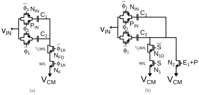
2 (b)Figure 4-11: Input sampling circuits. (a) Input sampling circuit of the first stage. (b) Input sampling circuit of the second through twelfth stages.
NF 3.04 µm/0.18 µm NF D 1.52 µm/0.18 µm N1 1.52 µm/0.18 µm N1D 0.76 µm/0.18 µm N2 3.0 µm/0.18 µm NIN 1.04 µm/0.18 µm PIN 3.2 µm/0.18 µm
Table 4.3: Sampling circuit transistor sizes
the bit decision comparators to store their results in latches. Phase φ1X passes the
bit decisions to the reference voltages. Phase φ11 controls the length of the preset
time P . Phase φ21 sets the duration of the charge transfer time E1+ E2.
4.2.5
Input Sampling
The input sampling performed in the first stage differs from the input sampling per-formed in all of the succeeding stages. The input sampling circuit of the first stage is shown in Figure 4-11(a). The first stage input sampling circuit uses the standard bottom plate sampling technique [22, 23] to minimize input dependent charge
injec-tion. When input sampling switches consisting of NIN and PIN turn off the amount
of charge they inject on to the sampling capacitors, C1 and C2, depends on the input
voltage vIN. This input dependent charge corrupts the voltage sampled on to C1 and
C2 and creates overall circuit nonlinearity. Turning off transistor NF before turning
off the sampling switches locks the charge on the sampling capacitors and prevents the charge injected from the sampling switches from disrupting the sampled voltage. Transistor NF also injects charge as it turns off. Some amount of this injected charge
can also be input dependent. When NF turns off, the charge in its inversion layer
splits between its source and its drain. The proportion of charge that exits from its source and drain depends on the impedances seen from these two nodes. The impedance seen from its drain depends on the input voltage, therefore the charge in-jected from the drain of NF on to the bottom plate of C1 and C2 also depends on the
input voltage. The amount of input dependent charge injected from NF is much less
than the input dependent charge that would be injected by NIN and PIN. Adding a
dummy device NF D to the bottom plate of the sampling capacitors reduces the total
charge injected from the sampling switch NF on to the sampling capacitors [37]. As
NF turns off NF D turns on and absorbs the charge injected by NF. The details of the
transistors sizes is shown in Table 4.3. The sampling switch NF is sized to minimize
charge injection while still enabling adequate settling time.
The input sampling circuit used in all of the stages succeeding the first stage is shown in Figure 4-11(b). This circuit differs from the circuit in the first stage in two ways: the sampling switch N1 is controlled by the comparator output of the previous
stage S and a switch N2 is placed in parallel with the sampling switch. Transistor
N2 is only on during the coarse charge transfer phase. During this phase a large
current passes through the switch potentially creating a large voltage drop across it. The parallel device N2 lowers the overall switch impedance and consequently lowers
the voltage drop across the switch. The charge injected by N2 is sunk by N1 to
VCM during the fine charge transfer phase and consequently has no effect on the final
through the sampling switch N1 creating a smaller voltage drop. The sampling switch
N1 can consequently be narrower and have a larger resistance. The charge it injects
can potentially disrupt the sampled charge as mentioned above. The sampling switch N1 is sized small so that it injects a minimum amount of charge.
4.2.6
Layout
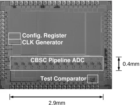
The die photo in Figure 4-12 shows the overall layout of the chip. The pipeline consists of 13 identical stages. The last stage does not resolve any bits. It just provides the correct load to the 12th stage. The outputs of only the first 10 stages were used in testing. The 11th and 12th stages were included in case the ADC had linearity and noise performance exceeding 10 bits. The chip also contains a configuration register, a clock generator and a test bit decision comparator. The area of the pipeline is 1.2 mm2 while the area of the overall chip is 10.9 mm2. The total chip area is much
larger than the pipeline because the design required a large number of pads for testing flexibility and because the pipeline was not folded. Most of the pads were used by bit outputs. All of the raw bit outputs were taken off chip and reduced from 24 to 12 using MATLAB. In order to avoid design complexity the pipeline was laid out in a line rather than being folded into two lines. This was done so that each stage would see the same capacitance and therefore could use the same currents. If the pipeline was folded the stage directly before the fold would see more output capacitance than all of the rest. It would therefore have required a unique design or unique bias voltages. The layout of a single stage of the ADC is shown in Figure 4-13 and a stage floor plan is shown in Figure 4-14. Since the ADC is a single ended design, the stage is not laid out in a symmetric fashion. Only the bit decision and threshold detection comparators are laid out symmetrically because they are differential circuits. The two sampling capacitors are each divided in two and laid out in a cross-quad with dummy capacitors surrounding them. This layout technique minimizes the potential for capacitor mismatch. The clock lines and bit lines are located at the top of the stages far away from the sensitive analog nodes to prevent coupling from the digital
2.9mm
0.4mm
Figure 4-12: Die photograph. 0.18 µm CMOS process. Pipeline Area: 1.2 mm2.
to the analog circuits. All of the sensitive analog circuits are ringed with n-wells and substrate connections to minimize substrate noise coupling. The most sensitive nodes such as the input to the continuous time comparator are shielded on all sides by metal to prevent stray signals from coupling on to them.
DVDD/GND BULK CLOCKS Bit Drivers DVDD/GND Clock Drivers Bit Decision Compartor BitLogic Bit Decision Comparator BitLogic
VDD/GND
BULK
Level Detection
Compartor Level DetectionLogic
reference switches Caps Input Switches Reference Switches VDD/GND BULK VDD/GND VDD/GND BULK References Current Sources References