HAL Id: hal-03266265
https://hal.archives-ouvertes.fr/hal-03266265
Submitted on 21 Jun 2021
HAL is a multi-disciplinary open access
archive for the deposit and dissemination of sci-entific research documents, whether they are pub-lished or not. The documents may come from teaching and research institutions in France or abroad, or from public or private research centers.
L’archive ouverte pluridisciplinaire HAL, est destinée au dépôt et à la diffusion de documents scientifiques de niveau recherche, publiés ou non, émanant des établissements d’enseignement et de recherche français ou étrangers, des laboratoires publics ou privés.
Field Grading Composites Tailored by
Electrophoresis-Part 2: Permittivity Gradient in
Non-Uniform Electric Field
S. Diaham, Z. Valdez-Nava, T. Le, L. Lévêque, Lionel Laudebat, T. Lebey
To cite this version:
S. Diaham, Z. Valdez-Nava, T. Le, L. Lévêque, Lionel Laudebat, et al.. Field Grading Compos-ites Tailored by Electrophoresis-Part 2: Permittivity Gradient in Non-Uniform Electric Field. IEEE Transactions on Dielectrics and Electrical Insulation, Institute of Electrical and Electronics Engineers, 2021, 28 (2), pp.341-347. �10.1109/TDEI.2020.009031�. �hal-03266265�
Field Grading Composites Tailored by Electrophoresis – Part 2:
Permittivity Gradient in Non-Uniform Electric Field
S. Diaham
1, Z. Valdez-Nava
1, T. T. Le
1, L. Lévêque
1, L. Laudebat
1,2and T. Lebey
11LAPLACE, Université de Toulouse, CNRS, INPT, UPS, Toulouse, France 2Université de Toulouse, INU Champollion, place de Verdun F-81012 Albi, France.
ABSTRACT
A series of three articles present an innovative way to build advanced functionally graded materials (FGM) based on polymer/ceramic composites tailored by electrophoresis from the process principle to their field grading application in power electronics. In this Part 2, it was studied the impact of a non-uniform electric field on the high-k SrTiO3 particle
organization within an epoxy matrix. In that purpose, DBC substrates with sharp metallization tracks were used to generate a strong electric field divergence. This non-uniform field has been used to organize the particles around the field reinforcement regions during the electrophoresis process. It was discovered that the particles self-arrange into a conformal composite FGM layer that presents a local permittivity gradient: the highest ε being located around the electric field peak areas. This new process could be used to selectively ‘heal’ the electric field-induced weaknesses of any high voltage electrical system by using its own design.
Index Terms — functionally graded materials (FGM), composites, electrophoresis,
insulation, encapsulation, high voltage, field grading, power electronics module
1
INTRODUCTION
THE unstoppable rise in the global electrical energy demand has as main consequence an increase in the power, and consequently in the working voltage, –and thereby of the working electric field–, of most of the electronic devices and systems participating to the electrical energy conversion [1, 2]. To continuously sustain the development of advanced higher voltage power systems, polymers and/or composite polymer-based materials, used to provide the sufficient electrical insulation between the high voltage (HV) metal parts and ground, have to be more and more robust. It is particularly true when a non-homogeneous electric field occurs for which the divergence is partly due to the sharp geometry of the electrode configuration [3].
For instance, polymeric materials involved as insulators in power electronics systems such as epoxy resin, polyimide, silicone gel or silicone rubber, can rapidly age when the electrical field overcomes a certain threshold [4, 5]. This can lead to partial discharges, electrical treeing or even breakdown event.
Composite materials, based on mixing a polymer matrix filled with inorganic particles, appear in recent years more and more powerful in electrical insulation to improve the dielectric properties and to overcome the polymer limits (e.g. enhanced intrinsic performances, higher stability, longer
lifetime) [6-9]. So far, and especially, nanocomposites enable to slightly enhance the overall dielectric properties of these polymers and other ones [10, 11]. However, such an improvement could face a limit considering the continuous increase in the voltage and electric field in most of the applications.
Consequently, alternative material solutions are growing up through field grading materials, where the higher permittivity and/or conductivity properties of the materials are used as attenuation layers to mitigate the electric field [12, 13]. More interestingly, a very few researchers had developed field grading material concept by building them in a non-homogeneous distributed way: functionally graded
materials (FGM). FGM are a class of materials that are
tailored to have a spatial evolution of at least one property in one direction. In the case of composites, this is achieved by structuring a particle spatial distribution offering a property gradient in the initial isotropic matrix [14, 15]. Among the main research works of this topic, Okubo’s group has pioneered the development of FGM composites with particle distribution gradient processed by centrifugation force. These materials exhibit interesting permittivity gradient in the direction of the centrifugation force and have applications in HV gas-insulated switchgear for field relaxation [16, 17]. However, for power electronics systems (as power modules) with a more complex electrode design, the centrifugation process is no longer suitable to tailor locally a property gradient exactly where the electric field is
Manuscript received on 29 May 2020, in final form 30 November 2020, accepted xx Month 20yy. Corresponding author: S. Diaham
the most concentrated.
Previously in the Part 1 of this three-articles series [18], an innovative electrophoresis process to tailor a permittivity gradient within a polymer composite was reported (see Figure 1). The principle, process parameters and material properties were discussed when tailored under an homogeneous electric field using an electrode plane-plane configuration [19-21].
Figure 1. Impact of high permittivity particles arrangement in a polymer
composite on the permittivity gradient along a distance: (a) neat polymer, (b) particle homogenous distribution, (c) particle gradient distribution (FGM with gradient).
Presently in this Part 2, the same concept is discussed under a divergent electric field. Thus, the authors report how the particles self-organize themselves when their movement is induced by a sharp electrode configuration.
2 EXPERIMENTAL
2.1 MATERIALS AND COMPOSITE COMPOUNDS
The polymer used as the host matrix is a diglycidyl ether of bisphenol F (DGEBF) thermosetting epoxy resin. It is crosslinked using an amine-type hardener with a ratio of 10:1 (resin:hardener). The viscosity of the epoxy resin with harder is of 3000 mPa.s at room temperature and its density after curing is 1.23 g/cm3.
The high permittivity fillers used here are strontium titanate (SrTiO3) particles with a density of 5.11 g/cm3 and a
BET specific surface of 1.83 m2/g. SrTiO3 has the twofold
advantage of a negative Curie temperature that not interferes with the temperature application range, and of a higher dielectric strength (35 kV/mm) compared to BaTiO3 (5
kV/mm). They are polyhedral-shaped and have an average diameter of 600 nm. All the details can be found in ref. [18].
The composite mixture was elaborated by a direct blending process of the SrTiO3 particles (10 vol%) into the
liquid epoxy resin containing the hardener. The particles were then homogeneously dispersed within the matrix using a planetary mixer rotating at 3000 rpm for 8 minutes. The mixture was then degassed in primary vacuum (<1.5 kPa) before being poured on the electrophoretic test structures.
2.2 ELECTROPHORESIS PRINCIPLE
Electrophoresis is a physical process, which consists in
displacing particles within a liquid medium under the application of an electrostatic force (i.e. the Coulomb force) to the compound [22]. Trapping electric charges at the interface between the particles and the liquid enables the particles to move towards the electrode of opposite sign. To
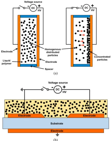
completely describe the transient regime of the layer formation, EHD (electro-hydro-dynamic) phenomenon should be taken into account [23]. In this paper, only is described the steady-state regime. Previously, the investigated FGM were obtained by applying a DC voltage on the liquid composite compound under uniform field (see Figure 2a). A consecutive thermal curing was performed in order to ‘freeze’ the particles where they have been accumulated.
(a)
(b)
Figure 2. Principle of the electrophoresis process under uniform DC
electric field (a). Same process using a lateral sharp electrode profile configuration on DBC substrate to induce a divergent electric field (b).
2.3 ELECTROPHORESIS IN DIVERGENT FIELD
In the current study, a modification of the electrode configuration from a plane-to-plane (uniform field) to a lateral sharp metallization’s profile one (divergent field) was implemented (see Figure 2b). This latter is typical of the electrode configuration found in power electronic modules where the copper metallization tracks are directly bounded and patterned with etching on ceramic substrates (DBC).
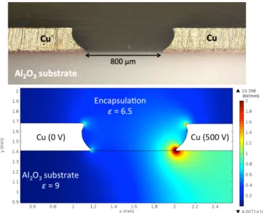
The DBC substrates used here were based on an alumina (Al2O3) ceramic substrate of 635 µm-thick metallized both
on top and bottom with 300 µm-thick copper layers. While the bottom Cu remained as a blank layer, the top Cu has been patterned, using a chemical etch through a mask, in the form of two tracks separated by a 1 mm gap in between them. The etching profile of the Cu layers is representative of those used as DBC substrates in power modules and presents a concave shape ending by sharp tip edges at the Al2O3 ceramic contact.
The tip-to-tip effective gap distance is thereby reduced down to 800 µm, as shown on the cross-section view in Figure 3a. After sealing this test structure with four side walls surrounding the tracks, the homogeneous epoxy/SrTiO3
liquid compound was poured to encapsulate the Cu tracks. An electrophoresis process was applied on the test structures involving a DC voltage set at 500 V for 15 min between the two top Cu tracks through soldered wires (not shown here in Figure 3, see Figure 2b). After switching the voltage off, the test structures were put into an oven at 150 °C for 20 min in air to crosslink the epoxy resin. Thus, accumulated and non-accumulated SrTiO3 particles were ‘frozen’ where they were
after DC voltage application. The curing process (both temperature plateau and rise time) has been optimized to be fast enough in order to mitigate particle sedimentation.
Figure 3. Cross-section of an Al2O3 DBC substrate used as a test structures
for divergent electrical field electrophoresis experiments (a). FEM simulation of the electric field reparation across the test structure submitted at an electrophoresis voltage of 500V (b).
2.4 ELECTRIC FIELD SIMULATION BY FEM
The finite element method used allows simulating the electric field distribution inside the structure. An electrostatic analysis has been performed by solving the Poisson’s equations, by using COMSOL Multiphysics to calculated the solution. In particular, the simulation provides quantitative results on the electric field.
Indeed, the exact shape of the DBC substrate has been designed under the simulation software and it should be noted that the maximum electric field at perfectly sharp edges is theoretically infinite, and thus a numerical solution simulation results are mesh-dependent.
For a more accurate analysis near the curved lines, the mesh was refined in these zones with a variable quadratic tetrahedral element for a more precise representation of the corner’s shape and tips [24]. Around the triple point zone, the mesh was refined to allow the calculation of the electric field every 0.4 μm. The applied potential on the metallization was 500 V while the non-covered and counter electrodes were both grounded.
3 RESULTS
AND
DISCUSSION
3.1 ELECTRIC FIELD DIVERGENCE AROUND DBC SUBSTRATES
Using this DBC electrode configuration, the electric field is no longer uniform like it could be in a classical plane-plane electrode one. Figure 3b shows the electric field distribution of a cross-sectioned DBC substrate modeled by finite element method (FEM) when it is initially encapsulated with the homogeneous epoxy/SrTiO3 of 10 vol% (permittivity
e=6.5).
It this case, there are two main reasons to induce a field divergence. The first one is related to the sharp edge of the Cu metallization that strongly enhances the electric field at the closest facing electrode tips by a pure geometrical effect (i.e tip-to-tip configuration). By this sharp-edge effect, the field is also enhanced around the top corners of the Cu tracks. On the other hand, the electric field divergence is further enhanced at the electrode tips by the ‘triple point’ effect where the junction of three different materials with different dielectric properties (i.e. metal, ceramic and composite) is located. The electric field around the HV electrode (Figure 3) is higher because there is the bottom electrode of the DBC connected at the ground potential (Figure 2b).
While the equivalent uniform electric field would have been of 625 V/mm with 500 V applied across an effective gap of 800 µm between parallel electrodes, the present divergent field is actually enhanced up by the spike effect around the HV electrode tips. Although the field is partly located into the Al2O3 ceramic, the highest electric field
region is refracted into the encapsulation, which has the lowest permittivity. Even if the electric field at the tip is theoretically infinite, in the vicinity of the tip high electric field values in the range of 2 kV/mm are observed. Such a non-uniform field distribution should obviously impact the particle movement and accumulation close to the HV electrode.
3.2 PARTICLE LAYER ACCUMULATION UNDER A NON-UNIFORM ELECTRIC FIELD
As reported in [18] in a plane-plane configuration, low electric field values (100-500 V/mm are largely enough to initiate the SrTiO3 particle movements within the liquid
epoxy resin and to collect them at the HV electrode over time. Presently, the sharp electrode configuration has as main consequence to concentrate further the particles around the highest electric field regions (i.e. around the tip regions).
Figure 4. Cross-section optical microscope image of cured epoxy/SrTiO3
composites without and with electrophoresis process at 500 V: (top image) randomly-dispersed composite and (bottom image) FGM composite with electrophoresis.
Figure 4 shows cross-section optical microscope images of cured epoxy/SrTiO3 composites processed with and
without electrophoresis. Thus, an accurate comparison of the particle distributions with the epoxy matrix can be made. While the randomly-dispersed composite presents a good and homogeneous distribution of the SrTiO3 particles in the
entire bulk, the FGM composite is made up of a non-conformal particle layer with high permittivity that accumulates around the HV electrode. The coating mainly occurs around the two sharp tips where the field reinforces the most in the DBC test structure (see Figure 3b). Moreover, on the HV electrode top side, one can observe a progressive decrease in the FGM layer thickness. Such a thickness reduction can be explained by the fact that the electric field viewed by the particles in this region progressively decreases as soon as they are far enough from the inter-electrode gap until becoming insignificant. As the FGM layer thickness is directly correlated to the field-dependency [18], it becomes understandable that the accumulated layer thickness on the DBC electrode top side is decreasing until zero.
Nevertheless, the concave shape of the Cu metallization tracks in the inter-electrode gap has unexpectedly collected a large amount of particles. Actually, this curvature zone, which does not correspond initially to the highest electric field region, seems presenting an important layer thickness as well. This might be explained by a preferential piling region for the particles occurring when the electric field dynamic is modified. The first accumulated particles could participate to minimize further the field around the sharp corners making the curvature region a novel collecting particles location. This entire particle layer could have been built progressively by trying to minimize at each moment the electric field.
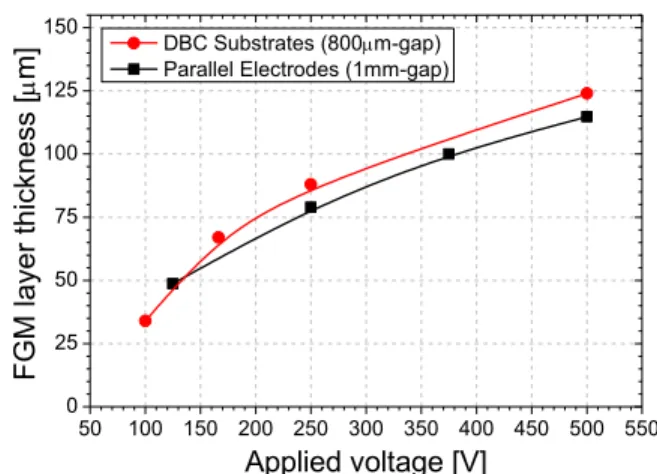
Figure 5. Thickness dependency of the accumulated particle layer versus
the applied voltage for 15 min for uniform and non-uniform electrode test structures (for DBC, the thickness is measured in the inter-electrode space at a height of 150µm from the ceramic surface). Data for parallel electrodes are taken from [19].
The thickness dependency of the accumulated particle layer in the gap of the DBC test structures has been evaluated for different applied voltages (for 15 min) and the results are shown in Figure 5. When comparing these data obtained in non-uniform field with those in uniform field extracted from [18], one can observe that the accumulated layer is thicker for a given voltage when the electric field is non-uniform. Here also, the thickness increases by following an electric field dependency and this highlights that SrTiO3 particles
self-organize where the field is the highest.
3.3 PARTICLE DISTRIBUTION IN FGM LAYER IN NON-UNIFORM ELECTRIC FIELD
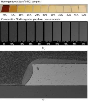
In order to understand further the internal structuration of the particles in the accumulated layer, the particle content distribution has been evaluated by developing an SEM imaging analysis technique. The method is based on firstly measuring accurately the grey level from backscattered electrons SEM images for a set of randomly-dispersed epoxy/SrTiO3 cross-sectioned flat samples (from 0 to 50
vol%), as shown in Figure 6a [25]. An image processing software was used in that goal. A normalized grey level master curve was obtained as a function of the filler content. Then, a 2D cartography of the grey level was measured on a cross-sectioned FGM composite processed on DBC substrate after electrophoresis (see Figure 6b). To avoid any artefact related to the incident electron beam setting parameters, all the samples were placed on the same holder and analyzed simultaneously during SEM.
50 100 150 200 250 300 350 400 450 500 550 0 25 50 75 100 125 150 DBC Substrates (800µm-gap) Parallel Electrodes (1mm-gap)
FG M laye r t hi ckne ss [ µ m] Applied voltage [V]
(a)
(b)
Figure 6. (a) Set of homogenous dispersed epoxy/SrTiO3 composited (by
5 vol%-step) and their respective cross-section SEM images for grey level measurement. (b) Cross-section backscattered electrons SEM image epoxy/SrTiO3 FGM composites after electrophoresis (500 V/15min).
Finally, a 2D-image reconstruction was performed using MATLAB®. Figure 7 shows what the SrTiO3 particle
concentration distribution looks like (by steps of 10 vol%) within and around the accumulated layer. The white regions correspond to the indicated filler content range. In the depleted region, the particle concentration has either not been affected (5-15 vol%) by the electric field or slightly affected (15-25 vol%). These observations are in good agreement with the low field magnitude in these zones (compared to Figure 3b). The 5-15 vol% range corresponds well to the initial filler content introduced in the epoxy resin (10 vol%). More interestingly, the accumulated layer presents an internal particle concentration distribution depending on the electric field magnitude viewed by each region. Therefore, the SrTiO3 particles self-organize in a density grading way
by following the electric field distribution. The highest the field, the more concentrated the particles.
Figure 7. 2D reconstruction of the SrTiO3 particle concentration
distribution within and around the accumulated layer. The white regions correspond to the indicated SrTiO3 volume content range. The two top
images show the density in the depleted region. The four middle images show the density within the accumulated layer. The bottom image is the overall particle distribution reconstruction.
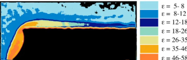
3.4 PERMITTIVITY GRADIENT SELF-ADAPTATION AROUND THE TRIPLE POINT
Figure 8. Permittivity of homogeneous composites as a function of SrTiO3
filler content. The inset shows the corresponding FGM permittivity gradient cartography calculated using the fitting curve.
As shown in [18], the permittivity of the accumulated layer is directly dependent on the applied electrophoretic field and thus on the particle concentration that results.
In order to assess the permittivity gradient within the FGM layer, dielectric spectroscopy measurements have been performed on flat homogeneous composite samples with accurately-known filler contents (like those from Figure 6a). Figure 8 shows the permittivity curve (measured at 20 °C, 1 kHz) versus the SrTiO3 filler content and the corresponding
fitting trend. Using the fitted trend, the SrTiO3 particle
concentration has been converted into a permittivity cartography around the DBC substrate metallization where one can clearly highlight a tailored permittivity gradient corresponding to the electric field distribution peaks, as shown in Figure 9. This self-structured permittivity gradient follows the electric fringe field and exhibits higher permittivity values around the electrode sharp corners (e>35) and decreases all along the FGM layer on the topside of the metallization until progressively reaching down e»6 (as for the randomly-dispersed composites). Complementary studies will have to be carried out to look at the impact of FGM structuration on mechanical and thermal properties.
Figure 9. 2D numerical reconstruction of the permittivity distribution
within and around the accumulated particle layer.
4 CONCLUSION
In this second paper of the series dealing with the development of advanced functionally graded materials (FGM) tailored by electrophoresis, it was investigated the impact of a non-uniform electric field on high-k SrTiO3
particle’s organization within an epoxy matrix. To exemplify this, DBC substrates, as those used in power electronic modules with sharp Cu metallization tracks, were used to generate a strong divergent electric field particularly around the tip regions (i.e. triple point and electrode corners). This non-uniform field, that typically induces electrical aging in HV applications, has been cleverly used to self-structure the particles around these field reinforcement regions during the electrophoresis process. Consequently, it has been discovered that the particles self-arrange into a conformal epoxy/SrTiO3 composite FGM layer. This layer locally
presents a permittivity gradient where the highest values are located around the electric field peak necessary to mitigate them. The next article, Part 3, of this three-articles series will present the impact of this permittivity gradient structuration on the field grading efficiency. This will be evaluated using electrostatic field modeling and breakdown voltage measurements of encapsulated power electronic DBC substrates.
ACKNOWLEDGMENT
The authors would like to thank the French Research National Agency (ANR) for funding this work in the frame of the ELECTRON project N°ANR-13-JS09-0007-01 (ANR JCJC 2013-2017).
REFERENCES
[1] V.G. Agelidis, G. Demetriades, and N. Flourentzou, “Recent Advances in High-Voltage Direct-Current Power Transmission Systems,” IEEE Int. Conf. Indus. Technol., 2006, pp. 206-213. [2] S. Ji, Z. Zhang, and F. Wang, “Overview of High Voltage SiC Power
Semiconductor Devices: Development and Application,” CES Trans. Electr. Mach. Sys., vol. 1, pp. 254-264, 2017.
[3] M.A. Fard et al, “Electrical Treeing in Cable Insulation under Different HVDC Operational Conditions,” Energies, vol. 11, 2406, 2018.
[4] J.-H. Fabian, S. Hartmann,, and A. Hamidi, “Analysis of Insulation Failure Modes in High Power IGBT Modules,” Proc. IEEE Ind. Appl.
Conf. (IAC), 2005, pp. 799-805.
[5] M. Sato et al., “Dynamic Potential Distributions of Surface Discharge in Silicone Gel,” IEEE Trans. Dielec. Electr. Insul., vol. 22, pp. 1733-1738, 2015.
[6] D.D.L. Chung, “Composite materials for electrical applications,” in
Engineering Materials and Processes, ed. B. Derby, Springer-Verlag,
London, 2003, pp. 73-89.
[7] Z. Li et al, “Effects of Nano-filler Addition on Partial Discharge Resistance and Dielectric Breakdown Strength of Micro-Al2O3/Epoxy
Composite,” IEEE Trans. Dielec. Electr. Insul., vol. 17, pp. 653-661, 2010.
[8] I. Plesa et al, “Properties of Polymer Composites Used in High-Voltage Applications,” Polymers, vol. 8, 173, 2016.
[9] N. Andraschek et al, “Mica/Epoxy-Composites in the Electrical Industry: Applications, Composites for Insulation, and Investigations on Failure Mechanisms for Prospective Optimizations,” Polymers, vol. 8, 201, 2016.
[10] S. Diaham et al, “Huge Nanodielectric Effects in Polyimide/Boron Nitride Nanocomposites Revealed by the Nanofiller Size,” J. Phys. D: Appl. Phys., vol. 48, no. 38, 2015.
[11] D. Tan and P. Irwin, “Polymer Based Nanodielectric Composites,” in
Advance in Ceramics – Electric and Magnetic Ceramics, Bioceramics, Ceramics and Environment, ed. C. Sikalidis, InTech, Rijeka, 2011, pp.
115-132.
[12] G. Mitic, T. Licht, and G. Lefranc, “IGBT Module Technology with High Partial Discharge Resistance,” IEEE Ind. Appl. Conf. (IAS), 2001, pp. 1899-1904.
[13] L. Donzel and J. Schuderer, “Nonlinear Resistive Electric Field Control for Power Electronic Modules,” IEEE Trans. Dielectr. Electr. Insul., vol. 19, pp. 955-959, 2012.
[14] N.J. Lee et al, “Characterization of Functionally Gradient Epoxy/Carbon Fiber Composite Prepared under Centrifugal Force,” J. Mater. Sci., vol. 32, pp. 2013-2020, 1997.
[15] M. Krumova, C. Klingshirn, F. Haupert, and K. Friedrich, “Microhardness Studies on Functionally Graded Polymer Composites,” Comp. Sci. Technol., vol. 61, pp. 557-563, 2001. [16] K. Kato et al, “Application of Functionally Graded Material for Solid
Insulator in Gaseous Insulation System,” IEEE Trans. Dielec. Electr. Insul., vol. 13, pp. 362-372, 2006.
[17] M. Kurimoto et al, “Application of Functionally Graded Material for Reducing Electric Field on Electrode and Spacer Interface,” IEEE Trans. Dielec. Electr. Insul., vol. 17, pp. 256-263, 2010.
[18] S. Diaham et al, “Field Grading Composites Tailored by Electrophoresis – Part 1: Principle and Permittivity Gradient in Uniform Electric Field,” IEEE Trans. Dielec. Electr. Insul., submitted, (same series)
[19] S. Diaham et al, “Method for processing an electrically insulating material providing same with self-adjusting electric field grading properties for electrical components,” no. WO2017211847A1, Dec. 14, 2017.
[20] L. Lévêque, “Nouveaux matériaux composites à gradient de permittivité structurés par un champ électrique et leur application pour la gradation de potentiel,” PhD dissertation, University of Toulouse, 2017.
[21] S. Diaham et al, “An Original Way to Tailor Field Grading Composite Materials with Permittivity Gradient by Electrophoresis,” IEEE Int.
Conf. Dielectric (ICD), 2018, pp. 1-4.
[22] L. Besra and M. Liu, “A Review on Fundamentals and Applications of Electrophoretic Deposition (EPD),” Progr. Mater. Sci., vol. 52, pp. 1-61, 2007.
[23] P. Atten and M. Haidara, "Electrical Conduction and EHE Motion of Dielectric Liquids in a Knife-Plane Electrode Assembly," IEEE Trans. Dielec. Electr. Insul., vol. EI-20, no. 2, pp. 187-198, April 1985. [24] L. Krähenbühl et al, “Numerical treatment of rounded and sharp
corners in the modeling of 2D electrostatic fields,” J. of Microwaves, Optoelectr. and Electromag. Appl., vol. 10, no.1, pp. 66-81, 2011. [25] L. Lévêque et al, “Effects of Filler Content on Dielectric Properties of
Epoxy/BaTiO3 and Epoxy/SrTiO3 Composites,” Annu. Rep. Conf.
Sombel Diaham (M’16) was born in 1982 in
Montauban, France. He was M.Sc. graduated in 2005 and received his PhD degree in 2007 in Electrical Engineering from University of Toulouse, France. In 2008, he joined the LAPLACE as Associate Professor. He received his Research Supervision Habilitation (HDR) from University of Toulouse in 2017. His research work deals with insulating polymers for high voltage power electronics.
Since 2009, he develops a research activity on composites (nanodielectrics and (di)electrophoretic-structured composites) for power electronics. Since 2018, he has been an invited researcher in Analog Devices, Limerick (Ireland), working on insulation design for HV digital isolators used in isolated-gate drivers. He co-authored 42 papers in international scientific journals, 68 papers presented in international conferences, 5 book chapters, 1 book as Guest Editor and 6 granted patents.
Zarel Valdez-Nava (M’16). He received his
PhD in Materials Science in 2005 jointly from University of Toulouse, France and the Autonomous University of Nuevo Leon, Mexico. In 2008, he joined the LAPLACE as Researcher of the French National Scientific Research Center (CNRS). His research work deals with insulating and dielectric materials for high voltage and/or for high temperature power electronics.
His interests concern the relationship between the processing of composite and ceramic materials in regards of their performance in real electrical engineering applications. He has co-authored over 30 papers in international scientific journals.
Louis Lévêque was born in 1989 in France. He
received his Engineering degree in Materials Science from the University of Nantes (Polytech Nantes) in 2012, and his PhD degree in Electrical Engineering from the University of Toulouse in 2017. He is contributed as PhD student in the framework of the ELECTRON-ANR project. From 2017-2019, he worked on the PROCETS European project at Tenneco, Belgium.
In 2020, he joined the High School Saint-Exupéry in Bellegarde-Sur-Valserine (Valserhône, France), where he is a teacher of Science and Technology in Industry and Sustainable Development.
Trung Trong Le was born in 1986 in Thanh
Hoa, Vietnam. He obtained his MSc degree in Electrical Engineering from Hanoi University of Science and Technology in 2009 and received the PhD degree from the University of Toulouse in 2016. He contributed as a post-doctoral researcher in the framework of the ELECTRON-ANR project. He is currently a research associate at Laplace Laboratory and research engineer at IRT Saint-Exupéry, France, working on application of FGM composites to power electronic modules.
Lionel Laudebat was born in Toulouse,
France, in 1974. Former student of the Brittany site of the Ecole Normale Supérieur de Cachan. He received the “Agrégation” in Electrical Engineering in 1998 and the PhD degree from the University of Toulouse III in 2003. He is currently an Associate Professor of Electrical Engineering at the University of Toulouse, Albi site (France).
He is associated researcher in LAPLACE since 2015. His main research interests include numerical simulation and modeling of power electronic
materials, studies of dielectric materials included modeling and characterization especially for ceramics and composite materials.
Thierry Lebey (M’98) received his M.Sc.
degree in Solid State Physics in 1984, his Ph.D. in Electrical Engineering in 1989, both from University Paul Sabatier in Toulouse. Since 1990, he is engaged with the French National Scientific Research Center (CNRS) where he is now Senior Research Scientist. He is the author of more than 80 journal and 130 conference papers and holds 10 international patents. From 2016 to 2019, he was Director of the Laboratory of Plasma and Energy Conversion - LAPLACE - in Toulouse. Since 2020, he is working as an high voltage expert for Safran Group.