HAL Id: cea-01974557
https://hal-cea.archives-ouvertes.fr/cea-01974557
Submitted on 8 Jan 2019
HAL is a multi-disciplinary open access archive for the deposit and dissemination of sci-entific research documents, whether they are pub-lished or not. The documents may come from teaching and research institutions in France or abroad, or from public or private research centers.
L’archive ouverte pluridisciplinaire HAL, est destinée au dépôt et à la diffusion de documents scientifiques de niveau recherche, publiés ou non, émanant des établissements d’enseignement et de recherche français ou étrangers, des laboratoires publics ou privés.
Conductivity via Thermally Induced Gap-States in a
Polyoxometalate Thin Layer
Qirong Zhu, Barbara Paci, Amanda Generosi, Séverine Renaudineau, Pierre
Gouzerh, Xihui Liang, Claire Mathieu, Cindy Rountree, Guillaume Izzet,
Anna Proust, et al.
To cite this version:
Qirong Zhu, Barbara Paci, Amanda Generosi, Séverine Renaudineau, Pierre Gouzerh, et al.. Con-ductivity via Thermally Induced Gap-States in a Polyoxometalate Thin Layer. Journal of Physical Chemistry C, American Chemical Society, 2019, 123, pp.1922-1930. �cea-01974557�
Conductivity via Thermally Induced Gap-States in a
Polyoxometalate Thin Layer
Qirong ZHU1,2, Barbara PACI4, Amanda GENEROSI4, Séverine RENAUDINEAU1, Pierre
GOUZERH1, Xihui LIANG3,6, Claire MATHIEU3, Cindy ROUNTREE5, Guillaume IZZET1,
Anna PROUST1, Nicholas BARRETT3, Ludovic TORTECH1,2
1Sorbonne Université, CNRS, Institut Parisien de Chimie Moléculaire, IPCM, 4 Place Jussieu, F-75005 Paris,
France
2LICSEN, NIMBE, CEA, CNRS, Université Paris-Saclay, CEA Saclay 91191 Gif-sur-Yvette Cedex, France 3SPEC, CEA, CNRS, Université Paris Saclay, F-91191 Gif sur Yvette, France
4ISM-CNR-Area di Ricerca di Tor Vergata, Via del Fosso del Cavaliere 100, 00133 Roma, Italy
5SPHYNX, SPEC, CEA, CNRS, Université Paris-Saclay, CEA Saclay 91191 Gif-sur-Yvette Cedex, France 6Guangzhou Research Institute of Opto-Mechano-Electrical technology, No. 3, Keyan Road, Guangzhou,
Guangdong, 510663, People's Republic of China
Abstract
We report a study of -[P2W18O62]6-, Wells-Dawson polyoxometalate layers deposited on ITO
coated glass substrates. A variety of techniques has been used including atomic force microscopy for surface topography characterization, current mapping and current-voltage characteristics, X-ray photoemission spectroscopy for chemical analysis, UV-visible photoemission spectroscopy for determination of band line-ups and energy dispersive X-ray reflectivity for determination of layer thicknesses and scattering length densities. The conditions of film deposition and subsequent thermal annealing strongly affect the film characteristics. In particular, we show that nanostriped films a few tens of nm thick can be obtained in a reproducible manner and that such structuring is accompanied by the appearance of gap-states and by a switch from an insulating to a conductive state. Current-voltage characteristics demonstrate that highly ordered films of K6[P2W18O62] allow electron flow only
into an organic photovoltaic device and show the conduction through it thanks to favorable band alignment between ITO, the gap states and the active photovoltaic layers.
Introduction
The heterostructure in an optoelectronic device is frequently described as an energy staircase favoring charge transport in the valence (holes) or conduction (electrons) bands through the device. Enhancement of charge carrier lifetime and mobility may be achieved by inserting appropriate interfacial layers (Ils) which therefore play a key role in improving power conversion efficiencies (PCEs) of organic light-emitting diodes (OLEDs) and organic photovoltaic (OPV) solar cells.1,2 A wide range of materials, including notably polymers and
metal oxides, has been used for interfacial layer engineering in organic solar cells (OSCs).3
With the development of inorganic interfacial layers and the implementation of novel architectures, organic electronics has now reached maturity and is primed for commercialization. However the complexity of such multilayer devices hinders in-depth understanding of interfacial electrical conduction so that optimization of charge transport and minimization of electron-hole recombination remain two key challenges in organic electronics.4-8
More generally speaking, metal oxides have a broad potential for applications not only in energy conversion and storage,9,10 but also in data storage.11 In comparison with organic
materials, they usually display better transport properties and stability in air, longer lifetimes and higher transparency,12-14 but they often require relatively high temperature thermal
annealing (higher than 200°C) that may be incompatible with organic electronic technology.
Within this context, polyoxometalates15,16 (POMs) currently attract growing interest as an
metal-oxo anions that are molecular analogues of metal oxides.17 More specifically, in view of
their remarkable electrochemical15,18,19 and photochemical20-22 properties, they are interesting
models for quantum-sized semiconducting oxides. Therefore, in addition to their application as catalysts, POMs – especially Keggin- and Wells-Dawson-type species – are increasingly used as molecular components in devices such as non-volatile memories,25-27 capacitors,28,29
OLEDs,30-32 and OSCs. In addition to molybdenum12,33,34 and tungsten35,36 oxides, POMs –
mainly Keggin-37-41 and Wells-Dawson-type40,41 molybdates and tungstates and also a few
lacunary42 and hybrid43 species, have been used as cathode or anode interfacial layers in
different architectures OSCs where they serve as electron or hole extraction layers, respectively, enhancing efficiency via energy level alignment.
While indium tin oxide (ITO) on glass is widely used as the top anode electrode in optoelectronic devices, up to now little consideration has been given to the insertion of a POM layer between ITO and the active layer. It is therefore necessary to study the properties of ITO/POM junctions. In a preliminary investigation we considered the behavior of a 140 nm thick layer of K6[P2W18O62], hereafter noted K6-P2W18.44 Here, we report the results of a more
detailed study. Layers of K6-P2W18 of different thicknesses have been deposited on ITO and characterized using various techniques, including conducting atomic force microscopy (c-AFM) to obtain topographic images and current maps, local spectroscopy to obtain current-voltage characteristics and the electronic band diagram, X-ray (XPS) and ultra-violet (UPS) photoelectron spectroscopy to probe the chemical composition, and energy dispersive X-ray reflectivity (EDXR) to estimate the local charge density. We have also considered the lithium salt, Li6[P2W18O62], and the acid form, H6[P2W18O62], hereafter noted Li6-P2W18 and
H6-P2W18, respectively, to study the influence of the POM counter-ion. We established the necessary conditions for obtaining highly structured POM layers. We found that the disorder-order transformation in thick layers is accompanied by the appearance of gap-states and by a
transition from an insulating to a conductive state. The possible origin and the role of the gap states are discussed. Finally, the integration of a 46 nm K6P2W18 film as a hole transporting layer (HTL) in a conventional ITO/HTL/P3HT:PCBM/LiF/Al OSC confirmed the assumptions inferred from C-AFM, XPS and UPS studies.
Experimental section
Materials
ITO coated glass substrates (75 Ω cm−1) were purchased from Solems and silicon substrates
from Siltronix. K6[-P2W18O62]·14H2O45 and Li6[-P2W18O62].33H2O46 were prepared
according to procedures reported in the literature with only minor modifications. The acid form H6[-P2W18O62].31H2O was obtained using the Drechsel method as reported in the Supporting
Information. Poly(3-hexylthiophene) (P3HT), [6,6]-phenyl-C61-butyric acid methyl ester (PCBM, purity 99.5%), dimethyl sulfoxide (DMSO, purity 99.9%), 1,2-dichlorobenzene (ODCB, purity 99%), and lithium fluoride (LiF, assay 99.99%) were all purchased from Sigma-Aldrich. Aluminum (Al, purity 99.5%) was bought from GoodFellow. All the chemicals were used as received without further purification.
Preparation of substrates
All substrates were cleaned following the sequential process: (i) in the case of glass/ITO, the ITO electrode was defined using an adhesive tape to protect the desired track. The unprotected part was etched using a mixture of Zn powder and 38% w/w HCl; (ii) the adhesive tape was removed and the substrate was cleaned with ethyl acetate; (iii) wet cleaning was achieved by sequential ultrasonic baths using first alkaline detergent solution (5% v/v in deionized water),
and then dichloromethane, ethanol and isopropanol (IPA), each for 10 min; (iv) the dried surfaces were exposed to UV-ozone treatment for 10 min. Once cleaned, the substrates were rapidly transferred into the glovebox for spin coating.
Preparation of POM films
The K6-P2W18 powder was dissolved in DMSO at a concentration of 100 mg/mL (2.2×10⁻²
M) for thick films and 10 mg/mL (2.2×10⁻³ M) for thin films. The Li6-P2W18 and H6-P2W18
powders were dissolved in DMSO at a concentration of 10 mg/mL (2.2×10⁻³ M and 2.3×10⁻³
M, respectively) for thin films. A 46 nm thick K6-P2W18 film was spin-coated from a 100 mg/mL solution in three steps: step 1 at 500 rpm for 30 s, step 2 at 900 rpm for 20 s and step 3 at 2600 rpm for 10 s. Thin K6-P2W18 (1.9 nm), Li6-P2W18 (2.2 nm) and H6-P2W18 (3.8 nm) films were spin-coated from 10 mg/mL solutions in two steps: step 1 at 500 rpm for 10 s and step 2 at 2600 rpm for 50 s. Then the spin-coating films were annealed on a hot plate at 140 C for 10 min in a nitrogen glovebox. Thicknesses were estimated by XPS taking in consideration the Beer-Lambert law and by AFM and scratch depth measurements (Figure S5).
Organic solar cell fabrication
A stacked (ITO/POM/P3HT:PCBM/LiF/Al) OSC was fabricated as follows. The POM film was first deposited onto ITO as described above, then a 100~150 nm active layer consisting of P3HT:PCBM (15 mg/mL of P3HT and 12 mg/mL of PCBM, blend in ODCB) was deposited onto the POM layer and subsequently annealed at 80 °C for 15 min under nitrogen in a glovebox. Then, the samples were placed into a high vacuum chamber (10-7 mbar) for
evaporation of LiF (1.2 nm, at a rate of 0.01 Å s−1) and Al (100-150 nm, at 0.5 Å s−1) through
Instrumentation
For surface morphology measurements, we used a Bruker ICON AFM in fast scan mode with a silicon tip (k = 4 N m−1, radius = 5 nm). For C-AFM and local spectroscopy studies, we used
an Agilent PicoLE AFM in current sensing mode with a Pt/Ir tip (k = 0.2 N m−1, radius = 20
nm) by applying a specific bias. XPS measurements were performed in an ultra-high vacuum chamber (pressure lower than 10−9 mbar) with a monochromatic Al Kα X-ray source (1486.7
eV) and a SPHERA-Argus analyzer (ScientaOmicron). The pass energy was 40 eV giving an overall energy resolution (photon bandwidth and spectrometer) of 0.4 eV. The binding energy scale was calibrated using the C 1s (C-C peak set at 284.8 eV). UPS data were obtained by using a HIS-13 He I source, h=21.2 eV (ScientaOmicron) and the work function was measured by applying a bias of –6.2 V to the sample during recording the photoemission threshold. The photo-electrical characterization of OPVs was performed using a xenon lamp, with a AMG1.5 filter calibrated at 80 mW cm−2.
EDXR measurements were performed to measure the film thickness, interface roughness and electron density.47 A polychromatic incident radiation produced by a W anode X-ray tube was
used as probe (operating energy range: 10-55 keV), and an energy sensitive Solid State High purity Ge-single crystal detector accomplished the signal detection.
Results and discussion
AFM characterization of POM films
We began by investigating the effect of thermal annealing on the surface texture of 46 nm thick K6-P2W18 films grown on various substrates. Figures 1b-d show the AFM topography of 46
nm K6-P2W18 films on glass, silicon and ITO substrates, respectively. The K6-P2W18 solid film on the glass substrate is rough and irregular; moreover, cracks are visible (Figure 1b). On the silicon substrate, large height variations are observed across the film; the surface is highly heterogeneous (Figure 1c). In contrast, the ITO substrate provides a POM film with limited height variations and, in addition, promotes the formation of highly ordered strip domains, each of which is at an angle of 90° with respect to its neighbors (Figure 1d), while silicon or glass show no evidence of strip ordering. This structuring process is reproducible and the domain size can attain 100x100 m². Two line profiles, on and off the strip on a well-structured K6-P2W18 film surface (Figure S3) reveal that strips are crossing plateau and valley, which indicates that the ordering process is not restricted to surface texturing but involves the formation of an anisotropic bulk phase. Several K6-P2W18 films with a thickness from 2 to 150 nm have been grown on glass/ITO but well-structured films have only been observed for thicknesses between 46 nm and 150 nm (Figures S3 and S4). According to our results (Figure 1 and Figures S1 to S4), the necessary conditions for obtaining highly ordered strip domains oriented at 90° with respect to one another are i) use of a glass/ITO substrate, ii) deposition from a solution in DMSO, iii) thickness larger than 46 nm and iv) thermal annealing at 140°C for 10 min.
Figure 1. (a) Schematic representation of the Wells-Dawson type polyoxoanion [P2W18O62]6-.
(b), (c) and (d) AFM topographic images of 46 nm K6-P2W18 films grown on glass (b), silicon (c) and glass/ITO (d) substrates. Topography (e) and current mapping (f) (bias = -600 mV) of a highly ordered K6-P2W18 film on glass/ITO.
The conductivity of an annealed 46 nm K6-P2W18 film was investigated by applying a negative bias of 600 mV between ITO and a platinum/iridium AFM tip. In such conditions, given the relatively large optical band gap (3.5 eV) of K6-P2W18 and the positions of the valence and conduction band edges, the film is expected to be insulating. However, the current map in Figure 1f reveals high conductivity in the ordered strips while the two rectangular domains without strips visible in Figure 1e are clearly insulating. Thus, the K6-P2W18 film switches
from an insulating to a conductive state under structuration. As discussed above, strips represent a long range bulk structuring process. They therefore appears indispensable to provide conducting paths for charge transport in thick K6-P2W18 layers.
XPS characterization of POM films and POM/ITO interfaces
First, a full XPS core level analysis of a well-ordered 46 nm K6-P2W18 film grown on glass/ITO was carried out. The P 2p and K 2p spectra are shown in Figures S8 and S9. The XPS W core level spectrum (Figure 2a) was fitted after subtraction of a Shirley background, using symmetric 30% Gaussian/70% Lorentzian functions and a full width half maximum (FWHM) of 1.0 eV. The W 4f7/2 and W 4f5/2 peaks at 35.8±0.1 eV and 38±0.1 eV Binding Energy (BE)
are typical for W in its highest oxidation state (W6+).48 There is no indication of W5+ at the
surface of the film.
Figure 2. Photoelectron spectroscopy of an annealed 46 nm K6-P2W18 film grown on a
glass/ITO substrate: XPS W 4f (a) and O 1s (b) core-level spectra.
The O 1s spectrum of the film is shown in Figure 2b. The asymmetric peak was deconvoluted into three components located at 530.8, 531.7 and 532.8 eV BE, hereafter respectively referred
to as Oeq, Opol and Owat explained below. The relative proportions of Oeq and Opol were angle
dependent whereas that of Owat remained constant. The highest energy peak Owat is attributed
to hydroxylated species, including most certainly residual water. It is worth mentioning that no measurable trace of solvent was detected (i.e. no sulfur 3p1/2 3p3/2). The two main components,
Oeq and Opol are associated with oxo ligands of the POM. There are nine non-equivalent types
of oxo ligands in the Dawson structure (Figure 1a).The 18 O=W, the 36 OW2 and the eight
central oxygen atoms are chemically different from each other49,51,51 and it is tempting to
attribute the component with the lowest binding energy to the more basic bridging oxo ligands and the median one to the less basic terminal oxo bonds. However, this assignment would not account for the angular dependence of the spectrum. Thus, assuming a preferential orientation of the POMs based on the highly ordered structure of the layer, we favor an assignment in which these two peaks are attributed to equatorial and polar oxo ligands, respectively (hence, the notations Oeq and Opol).
We then studied layers thin enough to probe simultaneously the POM layer and the ITO substrate. In addition to a 1.9 nm K6-P2W18 film, we prepared a 2.1 nm Li6-P2W18 film and a 3.8 nm H6-P2W18 film for investigation of the effect of the counter-ion. XPS survey spectra of these three films and of ITO are shown in Figure S10 while the W 4f and O 1s core level spectra are shown in Figures 3a-f. Deconvolution of the XPS W 4f7/2 spectra of 140°C annealed
thin films of K6-P2W18 (Figure 3b) and Li6-P2W18 (Figure 3d) reveals two components at 34.5
and 35.8 eV BE, representative of 5+ and 6+ W oxidation states, respectively.41 The W5+
component represents 13% of the total intensity for the K6-P2W18 film (7% for the Li6-P2W18 film) and has a slightly larger FWHM (1.2 eV) than the W6+ component. As no other reducing
agent is present, we postulate that ITO spontaneously injects electrons into the POM layer. The percentages of W5+ obtained from Figures 3d and 3b indicate that approximately one and two
electrons per POM have been transferred from ITO to the POM for the 1.9 nm and 2.1 nm films, respectively. On the other hand, no W5+ is seen in XPS spectra of thick films, whether annealed
or not (Figure S9a), which can be explained by the decrease in the concentration of negative carriers further away from the interface. The doping level, as evidenced by the W5+ signal, is of
the order of 1021 cm-3. Taking into account the band gap this would correspond to a depletion
region of the order of 1 nm, similar to the electron inelastic mean free path. The effect of such doping is therefore expected to be detectable only in the very thin POM layers. The variation of the W5+ concentration in function of the POM layer thickness is depicted in Figure 3g.
The reduction of K6-P2W18 films at the interface with ITO may be compared with the
spontaneous reduction of a (NH4)6-P2W18 film by aluminium.41 The observed differences
regarding the degree of reduction are due to the higher reducing power of Al in comparison with ITO.
Figure 3. (a-f) O 1s and W 4f XPS spectra of 1.9 nm K6-P2W18 (a,b), 2.1 nm Li6-P2W18 (c,d)
and 3.8 nm H6-P2W18 (e,f) films. (g) Variation of the percentage of W5+ as a function of layer
thickness.
In addition to the signal from the ITO substrate, deconvolution of the XPS O 1s spectra of the thin films measured at the same angle (Figures 3a, 3c, 3e) revealed the same three components (Oeq, Opol and Owat) as for the thick film (Figure 2b). However, the intensity ratios differ (Table
S1), highlighting the effect of the counter-ion on the structuration of the annealed POM layer, most probably on the in bulk orientation of the anions. The Oeq/Opol ratio increases going from
K+ to Li+ and then H+. Furthermore, assuming that the component at the highest BE (O
originates from residual water, this gives 12 H2O per POM for the K6-P2W18 and Li6-P2W18
layers, and 6 for the H6-P2W18 layer.
UPS characterization of POM films
To get further insight into the origin of the conducting nature of annealed POM films, we investigated their electronic structure using UPS. The valence band (VB) and the gap region up to the Fermi level of a well-structured 46 nm K6-P2W18 film on glass/ITO as well as those of bare glass/ITO are shown in Figure 4a. The position of the valence band maximum (VBM) as estimated from a linear extrapolation of the VB leading edge, is 3.3 eV with respect to the Fermi level for K6-P2W18 (Figure S7) and 2.9 eV ITO, thus there is a 0.4 eV valence band offset. In addition, we observed a photoemission signal between the VBM and the Fermi level, indicating the presence of filled gap states. By subtracting the ITO spectrum from that of the POM, we highlighted a signal specifically attributed to gap states in the POM layer (inset Figure 4b). It is worth noting that no gap state is observed in the absence of post-deposition annealing (see Figure S6). The most intense feature in the gap can be decomposed into two components which are fitted by Gaussian peaks located at 0.7 eV (peak 1) and 1.1 eV (peak 2) BE.
The spectra of the valence band (VB) and band gap region obtained for the 1.9 nm (K6), 2.2 nm (Li6) and 3.8 nm (H6) annealed films are presented in Figures 4c and 4d. The VBM energy is 3.4 eV BE for K6- and Li6-P2W18, and 3.3 eV for H6-P2W18, (Figure 4c), indicating that alkali metal counter ions (K+ and Li+) shift the VBM to slightly higher energy compared to H+.
Figure 4. (a) Valence band spectra of a thick (> 46 nm) annealed K6-P2W18 film on ITO, (b)
extraction and deconvolution of the gap state signal, (c) Spectra of thin K6-, Li6- and H6-P2W18 layers on ITO, (d) zoom on the energy region of the gap states, (e-f-g) deconvolution of the gap state signal into two components for each of the three thin layers, (h) intensity ratio of the two gap state components as a function of counter ion.
In the same way as for the analysis of the UPS data for the thick (46 nm) POM layer (Figure 4b), the spectrum of the ITO substrate was subtracted from those of the thin POM layers (Figure 4e-g). The UPS spectrum of the H6-P2W18 film (Figure 4g) shows a clear decrease in the gap state intensity compared to the K6-P2W18 (Figure 4e) and Li6-P2W18 (Figure 4f) films. As in the case of the 46 nm K6-P2W18 film, two states referred to as 1 and 2, pinned at 0.7 eV and 1.1 eV BE below the Fermi level, can be resolved in the gap for the thin K6-P2W18 and Li6-P2W18 films whereas gap state 2 is almost absent for the acid form. These results are reported in Figure 4h.The films are conducting, with the exception of that based on H6-P2W18 which is almost insulating. We conclude that gap states, especially gap state 2, are at least in part responsible for the observed increase in conductivity of the films under annealing.
The existence and the role of gap states in semiconductors and their interfaces are well documented but their origin often remains unclear. In molecular semiconductors, they may result from contact with another material, thermal annealing, charge injection, defects or modifications of the crystal structure.52 In the present case the origin of gap states is particularly
puzzling. Let us first consider the possibility of charge doping. As discussed above, electrons are injected from ITO into the POM film; however, the UPS (Figure 4b) and W 4f XPS (Figure 2) studies of annealed 46 nm K6-P2W18 films on ITO/glass substrate unequivocally show that the presence of gap states and W5+ are not correlated. We can therefore exclude W reduction as
the main cause for the existence of gap states in the thick films. Let us then discuss the possibility of structural defects in the Dawson structure. On the basis of IR data of catalytic studies, it has often been argued that reduction of POMs, especially polyoxomolybdates, is accompanied by the elimination of one or several bridging oxygens.53 In this respect it may also
been noted that unsaturated sites, namely defect structures when one or more metal-oxygen bonds around the same metal atom are broken while the latter remains connected to the defect
site are commonly considered as reactive intermediates in the Mars-van Krevelen type oxidation reactions catalyzed by POMs, especially H5PV2Mo10O40.54,55 The existence of oxygen
vacancies has been advanced to explain the observation of band gaps in SiO2/APTES/H3PW12O40/IPA stacks.29 However, while the presence of oxygen vacancies is
well-established in molybdenum and tungsten oxides, where they are associated with the appearance of new features below the Fermi level,33,35 as yet no oxygen-defect POM has been
reported. It should further be noted that thermal analysis of H6P2W18O6256,57 and
K6P2W18O6257,58 demonstrates that the {P2W18O62} structure is stable up to 450 °C.
Accordingly, the possibility of oxygen vacancies in our Dawson structure may be reasonably ruled out. Thus, considering that no significant chemical change, except partial reduction of tungsten at the near interface ITO/POM, is anticipated for the POM, the origin of the gap states is rather to be found in the change in film structure upon annealing. This view is further supported by the effect of solvent (DMSO vs. DMF and H2O; see Figures S1 and S2) and that
of the counter ions (Figures 3 and 4). Residual water may also play a role in the process. The OFF/ON conductivity switching should therefore rather be seen as a self-doping effect induced by the thermal annealing, the bulk structuration and residual water (and solvent) constituting the layer.
UPS displays a clear signature of electronic states which could be responsible for the enhanced conductivity in the POM films grown on ITO after thermal annealing. However, it does not shed any light on the spatial distribution of conductivity in the POM layers. Based on the C-AFM topography (Figure 1e) and current (Figure 1f) maps, we suggest that long-range ordering enables efficient conduction pathways as depicted in Scheme S1.
Correlation between local I-V and gap states
UPS shows that two gap states are pinned 0.7 and 1.1 eV below the Fermi level (Figure 2b). The position of the conduction band minimum (CBM) of K6-P2W18 can be deduced from the optical gap (Figure S13). In this way, band alignment between ITO and K6-P2W18 can be predicted. Local spectroscopy using C-AFM on a highly ordered K6-P2W18 film (Figure 5) was performed. In local spectroscopy, a positive bias on ITO would drive electrons from K6-P2W18 to ITO, while a negative bias on ITO would sweep electrons from ITO to K6-K6-P2W18 (Figure 5a). The aim is to probe the electron transfer under an external applied bias, which also results in band bending at the ITO/POM interface. The electron transport process is revealed by an I-V characteristic, shown in Figure 5b where five regions can be identified: 0 V V 1.5 V (area 1), V = 0 V (area 2), -0.9 V V -0.5 V (area 3), -1.6 V V -1.0 V (area 4) and V -1.8 V (area 5).
Figure 5. (a) Schematic diagram of local spectroscopy with AFM. (b) Current-voltage
characteristic of a thick (46 nm) well-structured K6-P2W18 film grown on glass/ITO with applied bias ranging from -3 V to +1.5 V. (c) Corresponding energy staircase.
The corresponding energy staircase associated with the junction is shown in Figure 5c and sheds additional light on the conduction mechanisms. In area 1 (Figure 5b) the current is null, which means an insulating state or a blocking diode behavior. With a positive bias, the energy barrier in bulk K6-P2W18 (Figure 5c area 1) increases and electrons from the tip are blocked by the conduction band offset with respect to the POM. Indeed with positive bias on ITO the gap states are unoccupied and the electron density is therefore localized in the valence band of the tip. When the bias is negative, electrons are injected into the gap states. From +1.5 V to -3 V, band bending in bulk K6-P2W18 is gradually reduced and then reversed. Under negative bias, there are two different electron transfer mechanisms. The slopes of the I-V plot in areas 3 and 4 suggest an increase in electron mobility, which reflects the gap state enhancement of conductivity in the POM layer. The presence of gap states allows electrons to flow from ITO to K6-P2W18 (Figure 5c, areas 2 and 3). With a high enough negative bias (below -1.8 V, area 5) the I-V plot is parabolic at first and then becomes linear (see Figure S11), reflecting an ohmic contact and full overlap of the CBs of K6-P2W18 and ITO. In this case, the Fermi level and the gap states are shifted into the CB, which modifies the conduction of the K6-P2W18 layer by removing the energy barrier.
Energy band diagram and integration in solar cell
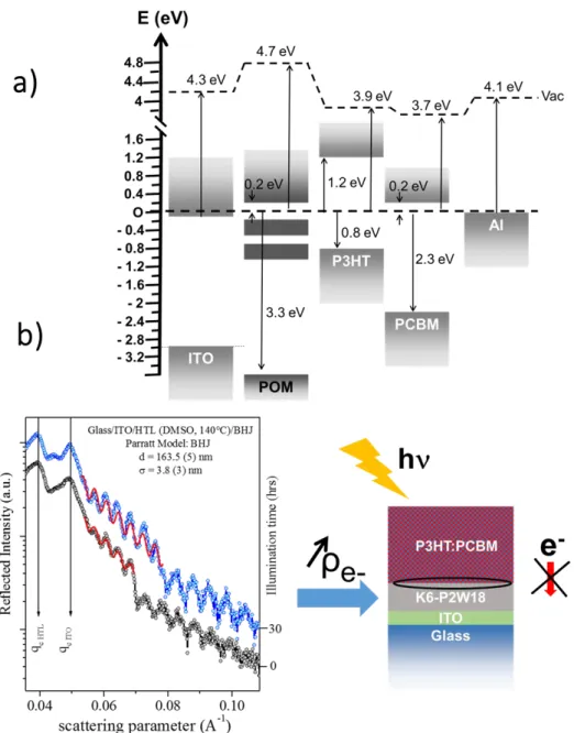
Highly ordered K6-P2W18 films on ITO show therefore a diode-like behavior. This suggests a charge transfer selectivity, only allowing electron flow from ITO to K6-P2W18 or, equivalently, hole injection from K6-P2W18 to ITO. The I-V characteristic from -1.8 V to 0 V demonstrates the role of the gap states in building an electronic bridge for hole injection into the ITO electrode at low bias. The ITO/POM band alignment can now be inserted into the overall band diagram
of a POV stack, as shown in Figure 6a, demonstrating the potential of the POM gap states to act as an electronic bridge gate between the highest occupied molecular orbital (HOMO) of P3HT to the CB of the ITO electrode.
EDXR was carried out to characterize the obtained OPV stack before and after illumination. The experimental conditions were optimized in order to enhance the bulk heterojunction (BHJ) signal; the P3HT-PCBM critical reflection edges and Kiessig fringes are well visible in Figure 6b. The P2W18 reflection edge was also observed, but Kiessig fringes arising from K6-P2W18 were not detected since they are masked by the contribution of the polymeric blend.
Figure 6. (a) Global energy band diagram of a P3HT:PCBM photovoltaic cell with the
K6-P2W18 thin film at the ITO interface, and (b) EDXR patterns of glass/ITO/K6-P2W18/P3HT:PCBM and best fits, black curve correspond to dark measurement and blue curve to the measurement performed under illumination.
Analysis of the reflectivity edges and electron densities of each contributing layer is reported in Figure S12.
From the Parratt fitting59 of the EDXR pattern in Figure 6b the morphological parameters of
the P3HT-PCBM BHJ are deduced (thickness d = 163.8 nm, roughness = 0.5 nm) in good agreement with the expected thickness given the film deposition conditions. The electron
densities of K6-P2W18 and of the BHJ were obtained in the dark state, corresponding to: HTL ρe = 3.04x10⁻⁵ Å-2 and BHJ ρe = 1.3x10⁻⁵ Å-2, in very good agreement with previously published
P3HT:PCBM results.47 No thickness or roughness variations were observed for the BHJ upon
illumination. However, some modification has occurred, indicating that illumination affects the electronic contrast at the interface. First of all, in the illuminated sample the first Kiessig fringe (0.04 A-1) of the HTL is now partially visible. Moreover, it is clear that the oscillation amplitude
has changed, which is confirmed by the Parratt fitting procedure. Indeed, the electron density of the HTL is now e = 3.20x10⁻⁵ Å-2, higher than in the dark state. On the other hand, the BHJ
electron density is constant, thus suggesting that the observed increase of the electron density concerns the HTL-ITO system.
Therefore, EDXR studies of the system {Glass/ITO/K6-P2W18/P3HT:PC60BM} detected an increase of the electron density at the K6-P2W18-ITO system under illumination. The excitons are generated under illumination and separated due to the P/N junction (P3HT:PCBM); the holes produced by the exciton separation are drained to the ITO while the absence of counter electrode induces the electrons accumulation in the POM responsible for the increase of the charge density. K6-P2W18 is a selective hole transport layer (blocking electron generated by the active layer under illumination). It can be denominated at the anodic ITO surface as a hole transport layer, HTL, thanks to the presence of gap states and N-Type semi-conductor characteristics. This provides confirmation of the hole injection phenomenon we observed from photoemission spectroscopy and local spectroscopy, i.e. the charge transfer between ITO/POM.
The photovoltaic performance using the K6-P2W18 film in a conventional P3HT:PCBM stack is presented in Figure S14. The first observation about the current voltage curve is that the POM can be successfully used as hole transport layer adjacent to the ITO. The performance of the cells obtained demonstrated of an increase of the open circuit voltage from 0.44 to 0.52 V on
built-in voltage, due to the gap states. The resulting performance of the cells reach 2.5% of power conversion efficiency. There also appears to be a slight decrease of the current density attributed the resistivity of the POM layer. This may imply not only the ability of the POM to drain efficiently holes from the active layer to the ITO but also that the gap states play a crucial role in the charge transport.
Conclusion
AFM, XPS and UPS, local spectroscopy and EDXR analyses were performed on several annealed and unannealed P2W18 films with different thicknesses and different counter-ions (K+, Li+, H+). We reproducibly obtained highly-structured K6-P2W18 films on glass/ITO
provided that they are i) deposited from POM solutions in DMSO, ii) thick enough and iii) post-annealed at 140 °C for 10 min. The formation of nano-stripes is accompanied by a switch from an insulating to a conducting state, the appearance of two gap states pinned at 0.7 and 1.1 eV below the Fermi level and also by an electron transfer from ITO to the POM layer – though this could not be directly demonstrated for thick films. We argue that the origin of gap states likely lies in the structuring process in which counter-ions and residual water play a crucial role. Gap states play a key role in the conduction mechanism(s). Integration of a structured K6-P2W18 film at the ITO anode of a {Glass/ITO/P3HT:PCPM/LiF/Al} stack confirms that it acts as a selective hole transport layer to ITO and results in an increase of the open circuit voltage from 0.44 V to 0.52 V.
AUTHOR INFORMATION
*E-mail: [email protected]. Phone: +33169086556
*E-mail: [email protected]. Phone: +33144273034
*E-mail: [email protected]. Phone: +33169083272
SUPPORTING INFORMATION
Supplementary materials is available in the supplementary information describing: the synthesis of H6[-P2W18O62].31H2O, providing additional AFM topographical studies, describing UPS analysis of an unannealed K6-P2W18 layer, and local spectroscopy performed by AFM, EDXR analysis, giving complementary surface and electronic analysis performed by EDXR, and finaly presenting the characteristics of the OPV devices.
ACKNOWLEDGEMENTS
The authors would like to thanks the région Ile de France and the DIM Nano-K for funding the PhD grant to Qirong Zhu.
References
(1) Steim, R.; Kogler, F. R.; Brabec, C. J. Interface Materials for Organic Solar Cells. J. Mater. Chem. 2010, 20 , 249962512.
(2) Ma, H.; Yip, H.-L.; Huang, F.; Jen, A. K.-Y. Interface Engineering for Organic Electronics. Adv. Funct. Mater. 2010, 20, 1371–1388.
(3) Yin, Z.; Wei, J.; Zheng, Q. Interfacial Materials for Organic Solar cells: Advances and Perspectives. Advanced Science 2016, 3, 1500362.
(4) Yu, X.; Marks, T. J.; Facchetti, A. Metal Oxides for Optoelectronic Applications. Nat. Mater. 2016, 15, 383–396.
(5) Yip, H.-L.; Hau, S. K.; Baek, N. S.; Ma, H.; Jen, A. K.-Y. Polymer Solar Cells That Use Self-Assembled-Monolayer- Modified ZnO/Metals as Cathodes. Adv. Mater. 2008, 20, 2376–2382.
(6) Yuan, Y.; Reece, T. J.; Sharma, P.; Poddar, S.; Ducharme, S.; Gruverman, A.; Yang, Y.; Huang, J. Efficiency Enhancement in Organic Solar Cells with Ferroelectric Polymers. Nat. Mater. 2011, 10, 296–302.
(7) Kim, J. Y.; Kim, S. H.; Lee, H.-H.; Lee, K.; Ma, W.; Gong, X.; Heeger, A. J. New Architecture for High-Efficiency Polymer Photovoltaic Cells Using Solution-Based Titanium Oxide as an Optical Spacer. Adv.
Mater. 2006, 18, 572–576.
(8) Gilot, J.; Barbu, I.; Wienk, M. M.; Janssen, R. A. J. The Use of ZnO as Optical Spacer in Polymer Solar Cells: Theoretical and Experimental Study. Appl. Phys. Lett. 2007, 91, 113520.
(9) Li, J.; Liu, Y.; Zhu, Z.; Zhang, G.; Zou, T.; Zou, Z.; Zhang, S.; Zeng, D.; Xie, C. A Full-Sunlight-Driven Photocatalyst with Super Long-Persistent Energy Storage Ability. Sci. Rep. 2013, 3, 2409.
(10) Wang, G.; Yang, Y.; Han, D.; Li, Y. Oxygen defective metal oxides for energy conversion and storage. Nano Today 2017, 13, 23-39.
(11) Ielmini. D. Resistive switching memories based on metal oxides: mechanisms, reliability and scaling. Semicond. Sci. Technol, 2016, 31, 063002.
(12) Sun, Y.; Takacs, C. J.; Cowan, S. R.; Seo, J. H.; Gong, X.; Roy, A.; Heeger, A. J. Efficient, Air-Stable Bulk Heterojunction Polymer Solar Cells Using MoOx as the Anode Interfacial Layer. Adv. Mater. 2011, 23, 2226–2230.
(13) Cowan, S. R.; Schulz, P.; Giordano, A. J.; Garcia, A.; MacLeod, B. A.; Marder, S. R.; Kahn, A.; Ginley, D. S.; Ratcliff, E. L.; Olson, D. C. Chemically Controlled Reversible and Irreversible Extraction Barriers Via Stable Interface Modification of Zinc Oxide Electron Collection Layer in Polycarbazole-Based Organic Solar Cells. Adv. Funct. Mater. 2014, 24, 4671–4680.
(14) Seo, H. O.; Park, S.-Y.; Shim, W. H.; Kim, K.-D.; Lee, K. H.; Jo, M. Y.; Kim, J. H.; Lee, E.; Kim, D.-W.; Kim, Y. D.; et al. Ultrathin TiO 2 Films on ZnO Electron-Collecting Layers of Inverted Organic Solar Cell. J.
Phys. Chem. C 2011, 115, 21517–21520.
(15) Pope, M. T. Heteropoly and Isopoly Oxometalates. Springer-Verlag Berlin, Heidelberg 1983.
(16) Pope, M. T.; Müller, A. Polyoxometalate Chemistry: An Old Field with New Dimensions in Several Disciplines. Angew. Chem. Int. Ed. Engl. 1991, 30, 34–48.
(17) Klemperer, W. G. Metal oxide chemistry in solution: the early transition metal polyoxoanions. Science
1985, 228, 533-541.
(18) Sadakane, M.; Steckhan, E. Electrochemical Properties of Polyoxometalates as Electrocatalysts. Chem. Rev. 1998, 98, 219–238.
(19) Ueda, T. Electrochemistry of Polyoxometalates: From Fundamental Aspects to Applications. ChemElectroChem 2018, 5, 823-838.
(20) Papaconstantinou, E. Photochemistry of Polyoxometallates of Molybdenum and Tungsten and/or Vanadium. Chem. Soc. Rev. 1989, 18, 1–31.
(21) Gómez-Romero, P. Polyoxometalates as Photoelectrochemical Models for Quantum-Sized Colloidal Semiconducting Oxides. Solid State Ion. 1997, 101–103, 243–248.
(22) Yamase, T. Photo- and Electrochromism of Polyoxometalates and Related Materials. Chem. Rev.
1998, 98, 307-326.
(25) Busche, C.; Vilà-Nadal, L.; Yan, J.; Miras, H. N.; Long, D.-L.; Georgiev, V. P.; Asenov, A.; Pedersen, R. H.; Gadegaard, N.; Mirza, M. M.; et al. Design and Fabrication of Memory Devices Based on Nanoscale Polyoxometalate Clusters. Nature 2014, 515, 545–549.
(26) Chen, X.; Zhou, Y.; Roy, V. A. L.; Han, S.-T. Evolutionary Metal Oxide Clusters for Novel Applications: Toward High-Density Data Storage in Nonvolatile Memories. Adv. Mater. 2018, 30, 1703950. (27) Hu, B.; Wang, C.; Wang, J.; Gao, J.; Wang, K.; Wu, J.; Zhang, G.; Cheng, W.; Venkateswarlu, B.; Wang,
M.; et al. Inorganic–Organic Hybrid Polymer with Multiple Redox for High-Density Data Storage. Chem. Sci. 2014, 5, 3404–3408.
(28) Herrmann, S.; Aydemir, N.; Nägele, F.; Fantauzzi, D.; Jacob, T.; Travas-Sejdic, J.; Streb, C. Enhanced Capacitive Energy Storage in Polyoxometalate-Doped Polypyrrole. Adv. Funct. Mater. 2017, 27, 1700881.
(29) Balliou, A.; Douvas, A. M.; Normand, P.; Tsikritzis, D.; Kennou, S.; Argitis, P.; Glezos, N. Tungsten Polyoxometalate Molecules as Active Nodes for Dynamic Carrier Exchange in Hybrid Molecular/Semiconductor Capacitors. J. Appl. Phys. 2014, 116, 143703.
(30) Palilis, L. C.; Vasilopoulou, M ; Georgiadou, D. G.; Argitis, P. A water soluble inorganic molecular oxide as a novel efficient electron injection layer for hybridlight-emittingdiodes (HyLEDs). Org. Lett.
2010, 11, 887-894.
(31) Tountas, M.; Topal, Y.; Kus, M.; Ersöz, M.; Fakis, M.; Argitis, P.; Vasilopoulou, M. Water-Soluble Lacunary Polyoxometalates with Excellent Electron Mobilities and Hole Blocking Capabilities for
High efficiency Fluorescentand Phosphorescent Organic Light Emitting Diodes. Adv. Funct. Mater.
2016, 26, 2655-2665.
(32) Ohisa, S.; Kagami, S.; Pu, Y.-J.; Chiba, T.; Kido, J. A Solution Processed Heteropolyacid Containing MoO3 Units as a Hole-Injection Material for Highly Stable Organic Light-Emitting Devices. ACS Appl.
Mater. Interfaces 2016, 8, 20946-20954.
(33) Vasilopoulou, M.; Douvas, A. M.; Georgiadou, D. G.; Palilis, L. C.; Kennou, S.; Sygellou, L.; Soultati, A.; Kostis, I.; Papadimitropoulos, G.; Davazoglou, D.; et al. The Influence of Hydrogenation and Oxygen Vacancies on Molybdenum Oxides Work Function and Gap States for Application in Organic Optoelectronics. J. Am. Chem. Soc. 2012, 134, 16178–16187.
(34) Soultati, A.; Douvas, A. M.; Georgiadou, D. G.; Palilis, L. C.; Bein, T.; Feckl, J. M.; Gardelis, S.; Fakis, M.; Kennou, S.; Falaras, P.; et al. Solution-Processed Hydrogen Molybdenum Bronzes as Highly Conductive Anode Interlayers in Efficient Organic Photovoltaics. Adv. Energy Mater. 2014, 4, 1300896.
(35) Vasilopoulou, M.; Soultati, A.; Georgiadou, D. G.; Stergiopoulos, T.; Palilis, L. C.; Kennou, S.; Stathopoulos, N. A.; Davazoglou, D.; Argitis, P. Hydrogenated Under-Stoichiometric Tungsten Oxide Anode Interlayers for Efficient and Stable Organic Photovoltaics. J. Mater. Chem. A 2014, 2, 1738– 1749.
(36) Vasilopoulou, M.; Soultati, A.; Argitis, P.; Stergiopoulos, T.; Davazoglou, D. Fast Recovery of the High Work Function of Tungsten and Molybdenum Oxides via Microwave Exposure for Efficient Organic Photovoltaics. J. Phys. Chem. Lett. 2014, 5, 1871-1879.
(37) Palilis, L. C.; Vasilopoulou, M.; Douvas, A. M.; Georgiadou, D. G.; Kennou, S.; Stathopoulos, N. A.; Constantoudis, V.; Argitis, P. Solution Processable Tungsten Polyoxometalate as Highly Effective Cathode Interlayer for Improved Efficiency and Stability Polymer Solar Cells. Sol. Energy Mater. Sol. Cells 2013, 114, 205–213.
(38) Jia, X.; Shen, L.; Yao, M.; Liu, Y.; Yu, W.; Guo, W.; Ruan, S. Highly Efficient Low-Bandgap Polymer Solar Cells with Solution-Processed and Annealing-free Phosphomolybdic Acid as Hole-Transport Layers. ACS Appl. Mater. Interfaces 2015, 7, 5367-5372.
(39) Zhu, Y.; Yuan, Z.; Cui, W.; Wu, Z.; Sun, Q.; Wang, S.; Kang, Z.; Sun, B. A cost-effective commercial soluble oxide cluster for highly efficient and stable organic solar cells. J. Mater. Chem. A 2014, 2, 1436-1442.
(40) Vasilopoulou, M.; Polydorou, E.; Douvas, A. M.; Palilis, L. C.; Kennou, S.; Argitis, P. Annealing-Free Highly Crystalline Solution-Processed Molecular Metal Oxides for Efficient Single-Junction and Tandem Polymer Solar Cells. Energy Environ. Sci. 2015, 8, 2448–2463.
(41) Vasilopoulou, M.; Douvas, A. M.; Palilis, L. C.; Kennou, S.; Argitis, P. Old Metal Oxide Clusters in New Applications: Spontaneous Reduction of Keggin and Dawson Polyoxometalate Layers by a Metallic Electrode for Improving Efficiency in Organic Optoelectronics. J. Am. Chem. Soc. 2015, 137, 6844– 6856.
(42) Tountas, M.; Topal, Y.; Polydorou, E.; Soultati, A.; Verykios, A.; Katzoglou, A.; Papadopoulos, T. A.; Auras, F.; Seintis, K.; Fakis, M.; et al. Low Work Function Lacunary Polyoxometalates as Electron Transport Interlayers for Inverted Polymer Solar Cells of Improved Efficiency and Stability. ACS Appl. Mater. Interfaces 2017, 9, 22773-22787.
(43) Tountas, M.; Topal, Y.; Verykios, A.; Soultati, A.; Kaltzoglou, A.; Papadopoulos, T. A.; Auras, F.; Seintis, K.; Fakis, M.; Palilis, L. C.; et al. A silanol-functionalized polyoxometalate with excellent electron transfer mediating behavior to ZnO and TiO2 cathode interlayers for highly efficient and extremely stable polymer solar cells. J. Mater. Chem. C 2018, 6, 1459-1469.
(44) Alaaeddine, M.; Zhu, Q.; Fichou, D.; Izzet, G.; Rault, J. E.; Barrett, N.; Proust, A.; Tortech, L. Enhancement of Photovoltaic Efficiency by Insertion of a Polyoxometalate Layer at the Anode of an Organic Solar Cell. Inorg Chem Front 2014, 1, 682–688.
(45) Sakai, Y.; Ohta, S.; Shintoyo, Y.; Yoshida, S.; Taguchi, Y.; Matsuki, Y.; Matsunaga, S.; Nomiya, K. Encapsulation of Anion/Cation in the Central Cavity of Tetrameric Polyoxometalate Composed of Four Tritanium(IV)-Substituted -Dawson Subunits, Initiated by Protonation/Deprotonation of the Bridging Oxygens on the Intramolecular Surface. Inorg. Chem. 2011, 50, 6575-6583.
(46) Kato, C.; Nishihara, S.; Tsunashima, R.; Tatewaki, Y.; Okada, S.; Ren, X.-M.; Inoue, K.; Long, D.-L.; Cronin, L.. Quick and selective synthesis of Li6[-P2W18O62].28H2O soluble in various organic
solvents. Dalton, Trans 2013, 42, 11363-11366.
(47) Albertini, V. R.; Paci, B.; Generosi, A. Energy Dispersive X-Ray Reflectometry as a Unique Laboratory Tool for Investigating Morphological Properties of Layered Systems and Devices. J. Phys. Appl. Phys.
2006, 39, R461.
(48) Fleury, B.; Billon, M.; Duclairoir, F.; Dubois, L.; Fanton, A.; Bidan, G. Electrostatic immobilization of polyoxometallates on silicon: X-ray Photoelectron Spectroscopy and electrochemical studies. Thin Solid Films 2011, 519, 3732-3738.
(49) Filowitz, M.; Ho, R. K. C.; Klemperer, W. G.; Shum, W. Oxygen-17 Nuclear Magnetic Resonance Spectroscopy of Polyoxometalates. 1. Sensitivity and Resolution. Inorg. Chem. 1979, 18, 93–103. (50) López, X.; Bo, C.; Poblet, J. M. Electronic Properties of Polyoxometalates: Electron and Proton Affinity
of Mixed-Addenda Keggin and Wells−Dawson Anions. J. Am. Chem. Soc. 2002, 124, 12574–12582. (51) Pascual-Borràs, M.; López, X.; Rodríguez-Fortea, A.; Errington, R. J.; Poblet, J. M. 17O NMR Chemical
Shifts in Oxometalates: From the Simplest Monometallic Species to Mixed-Metal Polyoxometalates. Chem. Sci. 2014, 5, 2031–2042.
(52) Yang, J.-P.; Bussolotti, F.; Kera, S.; Ueno, N. Origin and Role of Gap States in Organic Semiconductor Studied by UPS: As the Nature of Organic Molecular Crystals. J. Phys. Appl. Phys. 2017, 50, 423002. (53) Eguchi, K.; Toyozawa, Y.; Yamazoe, N.; Seiyama, T. An Infrared Study on the Reduction Processes of
Dodecamolybdophosphates. J. Catal. 1983, 83, 32–41.
(54) Efremenko, I.; Neumann, R. Computational Insight into the Initial Steps of the Mars–van Krevelen Mechanism: Electron Transfer and Surface Defects in the Reduction of Polyoxometalates. J. Am. Chem. Soc. 2012, 134, 20669–20680.
(55) Khenkin, A. M.; Efremenko, I.; Martin, J. M. L.; Neumann, R. The Kinetics and Mechanism of Oxidation of Reduced Phosphovanadomolybdates by Molecular Oxygen: Theory and Experiment in Concert. Phys. Chem. Chem. Phys. 2018, 20, 7579–7587.
(56) Baronetti, G.; Briand, L.; Sedran, U.; Thomas, H. Heteropolyacid-Based Catalysis. Dawson Acid for MTBE Synthesis in Gas Phase. Appl. Catal. Gen. 1998, 172, 265–272.
(57) Sambeth, J. E.; Baronetti, G. T.; Thomas, H. J. A Theoretical–Experimental Study of Wells–Dawson Acid: An Explanation of Their Catalytic Activity. J. Mol. Catal. Chem. 2003, 191, 35–43.
(58) Comuzzi, C.; Dolcetti, G.; Trovarelli, A.; Cavani, F.; Trifirò, F.; Llorca, J.; Finke, R. G. The Solid-State Rearrangement of the Wells-Dawson K6-P2W18O62·10H2O to a Stable Keggin-Type Heteropolyanion Phase: A Catalyst for the Selective Oxidation of Isobutane to Isobutene. Catal. Lett.
1996, 36, 75–79.
(59) Parratt, L. G. Surface Studies of Solids by Total Reflection of X-Rays. Phys. Rev. 1954, 95, 359– 369.
![Figure 1. (a) Schematic representation of the Wells-Dawson type polyoxoanion [P 2 W 18 O 62 ] 6-](https://thumb-eu.123doks.com/thumbv2/123doknet/13186584.391612/9.892.161.747.113.772/figure-schematic-representation-wells-dawson-type-polyoxoanion-p.webp)