Automated Circuit Extraction from
Mask Descriptions of MOS Networks
RLE Technical Report No. 503
February 1984
Steven Paul McCormick
Research Laboratory of Electronics Massachusetts Institute of Technology
Cambridge, MA 02139 USA
This research was supported in part by the Bell Labs Fellowship in Applied Computer Science and in part by U.S. Air Force Contract F29620-81-C-0054.
-1-^_^_111^·1_-··LLI···-II_-I--..-I '
Automated Circuit Extraction from Mask
Descriptions of MOS Networks
by
Steven Paul McCormick
B.S., University. of Massachusetts/Amherst (1979)
Submitted to the
Department of Electrical Engineering and Computer Science in partial fulfillment of the requirements
for the degree of
MASTER OF SCIENCE
at the
Massachusetts Institute of Technology February 1984
C Massachusetts Institute of Technology 1984
Signature of Author
Department of Electrical Engineering and Computer Science
I I February 17, 1984 Certified by Jonathan Allen Thesis Supervisor Accepted by Arthur C. Smith Chairman, Department Committee on Graduate Students
1
-
-
$-_--_--- I`-1-1" ---_·--·lly--rrrrrms·L·L----XI-·-^ .-_--- ---IIIX-l -- __
1 C
Por
'4'
Automated Circuit Extraction from Mask
Descriptions of MOS Networks
by
Steven Paul McCormick
Submitted to the
Department of Electrical Engineering and Computer Science on February 17, 1984 in partial fulfillment of the requirements
for the Degree of Master of Science.
Abstract
An automated circuit extractor generates an equivalent circuit description of an integrated circuit (IC) entirely from the geometric mask information. By analyzing the circuit description, IC performance can be estimated without having the IC design implemented. This thesis presents a methodology for accurate extraction of interconnection resistance, inter-nodal capacitance, ground capacitance, and transistor dimensions-circuit parameters important in characterizing the speed, noise-immunity, and static performance of designs for modern MOS technologies. Extracting each circuit parameter follows a general, numerical extraction algorithm with high accuracy. However, where possible, the general algorithms are replaced with simple techniques that do not sacrifice accuracy but execute much faster. Vital to the extraction methodology is a geometric operation that decomposes regions into domains appropriate for specialized algorithms and general algorithms.
Thesis Supervisor: Jonathan Allen
Title: Professor of Electrical Engineering and Computer Science
2
Acknowledgments
I thank Jonathan Allen for the initial project suggestion, for his continued support and valuable recommendations and ideas on extraction.
I thank the users of EXCL who have tested the extraction methodologies, uncovered problems, and made suggestions for improvement. In particular, I thank Donald Baltus who made the first exhaustive test of EXCL.
I thank William Evans for his valuable discussions on extraction and future needs of MOS IC design.
Finally, I thank Robert Armstrong for HPORAW-the system that generated the figures in this thesis.
This research was supported in part by the Bell Labs Fellowship in Applied Computer Science and in part by U. S. Air Force Contract F29620-81-C-0054.
3
Table of Contents
Chapter One: Introduction 9
1.1 Overview of EXCL 10
1.2 Overview of Remaining Chapters 11
Chapter Two: Extraction Models for Integrated Circuits 13
2.1 NMOS Technology 14
2.2 Types of Circuit Analysis 16
2.3 Transistor Modelling 18
2.4 Interconnection Capacitance Modelling 22
2.4.1 Ground Capacitance 22
2.4.2 Inter-Nodal Capacitance 23
2.5 Interconnection Resistance 25
2.6 Modelling Distributed RC's 26
2.7 Modelling Fabrication Degradations 27
Chapter Three: Connectivity Extraction Algorithms 28
3.1 Decomposition of Mask Geometries 28
3.2 Sort by Maximum Y 30
3.3 Scan of Geometrical Objects 30
3.3.1 Reducing the Vertical Search 32
3.3.2 Reducing the Horizontal Search 32
3.3.3 Rescan Queue 34
3.4 Geometrical Object Intersection 35
3.4.1 Error Watches 43
3.5 Intersection Removal 44
3.6 Path, Switch, And Contact Creation 45
3.7 Circuit Element Calculation 47
3.7.1 Circuit Extraction 47
3.7.2 Network Cleaning 50
3.8 Connection of Network 51
3.8.1 Minimum Circuit Values 52
3.8.2 Connection 52
3.9 Output Format 53
Chapter Four: Resistance Extraction 56
4.1 Field Analysis of Electric Conduction 57
4.2 Finite Elements Techniques 58
4.2.1 Boundary Conditions 61
4.2.2 Direct Solution of V 62
4.2.3 Iterative Solution of V 63
4.2.4 Comparison of the Direct and Iterative Solutions 4.2.5 Calculation of Rd and Resistor Networks
4.2.6 Accuracy of the Finite Element Method 4.3 Resistance Calculation of Straight-Subregions
4.3.1 Current-Spreading Region
4.4 Stored Calculations of Commonly Occurring Shapes 4.5 Subdividing Geometric Regions
4.5.1 Locating Straight Subregions
4.5.2 Storing and Locating Library Subregions 4.6 Connecting Resistor Subnetworks
4.7 Geometric Information for Capacitance Extraction Chapter Five: Interconnection Capacitance Extraction
5.1 Inter-Nodal Capacitance
5.1.1 Subdivision of Capacitance Problem 5.1.2 Field Theory of Capacitance Calculation 5.1.3 Finite Element Techniques
5.1.3.1 Determination of Weighted-Green's Functions 5.1.3.2 Sources of Error in the General Method 5.1.4 Overlapping Conductors
5.1.5 Parallel Conductors
5.1.6 Library Shapes in Inter-nodal Capacitance Extraction 5.1.7 Distribution of Capacitance Among Resistor Nodes 5.1.8 Window Size Determination
5.2 Ground Capacitance
5.3 Summary of Capacitance Extraction Chapter Six: Transistor Size Extraction
6.1 Rectangular Transistors 6.2 Non-Rectangular Transistors
6.2.1 Straight Subregion Dimensions 6.2.2 Library Subregion Dimensions 6.2.3 Irregular Subregion Dimensions
6.2.4 Dimension Combination and Coherency Check Chapter Seven: Conclusions
7.1 Final Notes and Recommendations for Improvement Appendix A: Distributed RC Modelling with r-Ladders Appendix B: Band-Matrix Operations
B.1 Band-Matrix Storage
B.2 Gauss Elimination with Band-Matrices
8.3 Repeated Solution with Different Boundary Values Appendix C: Spherical Coordinate Simulations
5 65 65 68 69 70 71 71 73 74 76 77 79 80 81 82 84 87 93 94 95 97 98 100 101 103 105 105 106 107 107 108 108 110 112 113 116 116 118 118 120 _____l·_XI____ __
Table of Figures
Figure 1 - 1: Organization of EXCL 11
Figu re 2-1: Conductors in the NMOS technology 14
Figu re 2-2: NMOS technology 1t6
Figu re 2-3: Top view example of non-rectangular transistor. 19
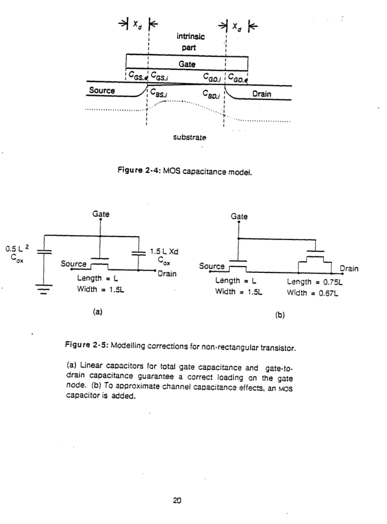
Figu re 2-4: Mos capacitance model. 20
Figu re 2-5: Modelling corrections for non-rectangular transistor. 20
Figu re 2-6: Capacitance types for interconnections. 22
Figure 2-7: Coupling capacitance between two nodes. 24
Figure 2-8: Connections for modelling tangential resistance. 26
Figu re 2-9: Pi-ladder networks for approximating distributed RC lines 27
Figu re 3- 1: Approximation for shapes with non-orthogonal edges 30
Figure 3-2: Major Program Modules of CONNECT 31
Figure 3-3: Bin Placement of Mask Objects 33
Figu re 3-4: Scanning process of a MOS transistor layout 34
Figure 3-5: Types of intersections 37
Figu re 3-6: A missed Metal-Cut intersection 38
Figu re 3-7: CMOS rule for error watches 43
Figu re 3-8: Rectangle conversion from random form to non-intersected form 44
Figure 3-9: Combination of Network Components 46
Figure 3-1 0: Cleaning Network Components 51
Figu re 3-1 1: Example Layout 53
Figu re 3-1 2: Complete Extracted Network of Example Layout 54
Figu re 3-13: Connected network 54
Figu re 3-14: Connected network with all resistors ignored 55
Figu re 4-1: Finite elements of a planar resistor 59
Figu re 4-2: Node designations for node i and its neighbors 59
Figu re 4-3: Resistor network analogy of a single finite element 61
Figure 4-4: Finite element resistor network 61
Figure 4-5: Network for direct solution example 62
Figu re 4-6: Number of iterations vs. one-dimensional finite element count. 66
Figu re 4-7: Completely connected resistor network 67
Figure 4-8: Conditions for combining connection regions 68
Figu re 4-9: Discretization error vs. finite element separation 69
Figu re 4-10: Current-spreading regions and maximum error estimates 70
Figu re 4- 1 1: Segment operations for isolating straight subregions 73
Figure 4-12: Straight regions hidden across two parallel rectangles. 74
Figu re 4-1 3: Library tree structure for four entries 75
Figu re 4-14: Resistance extraction of complete region 78
Figu re 5- 1: Capacitance types for a multi conductor system. 79
Figure 5-2: Complete capacitance network for a three conductor system 80
Figure 5-3: Subdivision of capacitance region. 82
Figure 5-4: Green's Theorem for finding V at point p 84
Figu re 5-5: Cross-sectional view of conductor geometries. 85
Figure 5-6: Finite element for inter-nodal capacitance extraction. 86
Figure 5-7: Shape functions for conductor shapes shown in inset 89
Figure 5-8: Field simulations for determining weighted-Green's functions. 90 Figu re 5-9: Weighted-Green's Functions vs. distance for a constant Shape Function 92
Figure 5-10: Simulation boundaries for diffusion conductor 93
Figure 5-1 1: Cross-section view of simulations for determining the fringe correction factor 95 Figure 5-1 2: Parallel capacitance functions for conductor shapes shown in inset. 96 Figure 5-13: Top view of capacitance calculations for determining the end correction 97
factor
Figu re 5-1 4: Subregions in inter-nodal capacitance library. 98
Figure 5-1 5: Distribution of inter-nodal capacitance among resistor nodes. 99
Figure 5-1 6: Flux lines from edge of target conductor 101
Figu re 6-1: Samples of transistors with calculable dimensions 106
Figu re 6- 2: Entries of transistor dimension library 107
Figure 6-3: Samples of transistors that cannot be sized 109
Figure 7-1: 7r-ladder network 113
Figure 7-2: Rectangular region divided into two-dimensional node grid 117
Figure 7-3: Band matrices 117
Figure 7-4: Setup of finite element analysis for determination of Greens's functions. 120
7
Table of Tables
Table 2-1: Capacitance values for non-rectangular transistor 21
Table 2-2: Sample capacitance constants for NMOS process 24
Table 2-3: Sample sheet resistances for NMOS process 25
Table 3-1: Intersection checks for example NMOS process 36
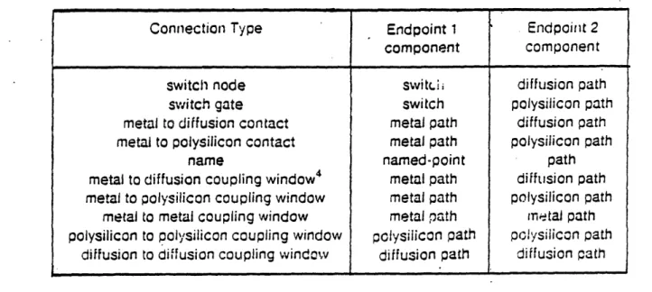
Table 3-2: NMOS connection types 46
Table 3-3: Extraction Library Procedures 48
Ta ble 4- 1: Sample library shapes and equivalent networks for NMOS process 72 Table 5-1 : Series of weighted-Green's functions for two conductors on different layers. 91
Table 5-2: Capacitance extractor parameters 104
Table 7- 1: Relative error of minimum pole for n-stage r-ladder 115
Table 7-2: Summary of approximate operation count and memory needs for gauss 119 elimination
CHAPTER ONE
Introduction
An integrated circuit designer generally wishes to locate and fix circuit design problems before dedicating his design to the expensive IC fabrication line. Inadequate speed, degraded logic levels, and excessive noise are just some of the circuit problems that plague the IC designer. Not too many years ago. extracting active device and connectivity information was sufficient to characterize the IC's circuit behavior. However, as IC structures are scaled down in size, problems associated with IC interconnections become particularly acute, for the effects' from parasitic resistances and capacitances begin to dominate over device effects. Today, a necessary step in locating potential circuit problems is extracting equivalent circuits for active devices and interconnections.
Previous computer programs have been written 1, 2, 3] for extracting transistor information and interconnection capacitance formed by overlapping layers. These extractors are proficient in verifying logical correctness, but not circuit performance correctness. None extract arbitrary inter-nodal capacitance information, and only one program [11 attempts to extract interconnection resistance information. To locate circuit problems, the IC designer must extract a complete spectrum of circuit parameters including interconnection resistance, ground capacitance (capacitance to the substrate), inter-nodal capacitance (or coupling capacitance), transistor sizes, and transistor areas. This is particularly true for designers of "analog sensitive" circuits such as random access memories, sense amplifiers, or bootstrap drivers.
General numerical techniques are known for solving each extraction problem in the spectrum [4]. The term "general" in this case is attached to methods that work for arbitrary shapes. Some of the general techniques-most notably for resistance and inter-nodal capacitance-are limited to very small problems because of their need for vast computing resources. In order to extract larger designs, automated circuit extractors have been developed [5] which use simpler techniques that do not solve the general problem. While the techniques are usually good for long, rectangular field regions, they sacrifice considerable accuracy around irregular regions.
9
--This thesis describes an automated circuit extractor, EXCL (EXtractor of Circuits from Layouts), that extracts complete interconnection and transistor information. It uses a range of extraction techniques for each problem-some are special-case and fast, others are general and slow. In the resistance, inter-nodal capacitance and transistor sizing problems, a single and powerful algorithm separates field regions into subregions of three kinds. Where the fields are one-dimensional (as the fields describing conduction in a long straight wire) one kind of subregion is formed, and the problem is solved using a simple equation. Of the remaining subregions, those with prespecified, commonly-occurring shapes have their solution found in a library. Only those subregions that cannot be solved with the previous two techniques use general techniques. Separating the problem in this way allows
EXCL to operate with reasonable speed without sacrificing accuracy. This gives EXCL the capacity to detect potential circuit hazards in larger IC designs containing sensitive circuits.
1.1 Overview of EXCL
EXCL converts raw mask geometric data generated by the IC designer into an equivalent circuit representation for subsequent simulation or analysis. An important feature of EXCL is its programming modularity. The program is not bound to any specific IC fabrication process or mask set specification, for all technology related instructions reside in two easily-modified program modules.
Figure 1-1 shows the general organization of EXCL. It is broken into a connectivity extractor part and an extraction library part. The connectivity extractor processes geometric mask information into isolated regions associated with individual circuit elements. This is controlled by one of the technology dependent modules. Next, the other technology dependent module, EXTRACT, instructs EXCL on how to convert geometric data into circuit data. It does so by calling on extraction algorithms contained in the extraction library. For instance, the user can include a command in
EXTRACT that says: for each region of a certain layer, activate the extraction library's "resistance extractor" to convert geometric data into resistor network data. By allowing the user to make such decisions, he can tailor the extractor to meet his own needs, i.e., he can make his own extraction
model.
Each of the basic extraction problems is self-contained in the extraction library. The library includes procedures for computing resistance, coupling capacitance, transistor sizes, and other parameters based on a region's area or perimeter.
10
geometric file geometric modules
Ni
circuit formatting modules circuit file IT' coupling capacitance extractorConnectivity Extractor Extraction Library
Figure 1 -1: Organization of EXOL
1.2 Overview of Remaining Chapters
The thesis is presented in three main parts. The first part (chapter 2) introduces an NMOS fabrication technology, and discusses each of the relevant circuit parameters that might be extracted. This part presents some of the basic issues that a designer must consider when developing an
extraction model for EXTRACT.
The next part (chapter 3) discusses the connectivity extractor of EXCL. It discusses the geometric and circuit portions of the connectivity extractor, including the two technology dependent modules.
The last main part (chapters 4 through 6) presents in detail each of the extraction algorithms for extracting resistance, interconnection capacitance, and transistor sizes. Some of the extraction algorithms are well-known, while others-most notably for coupling capacitance-had to be
11 resistance extractor EXTRACT EXTRACT-LIBRARY transistor size extractor ' II
I
11 II I II I II I II I I II I I I I I .4 -__e Jl - t - --'---"I~--~-~U~II^'II'~-li-- Ideveloped for EXCL. The basic algorithm for dividing a region into its subregions with different solution techniques is similar for each of these problems. The main discussion of the algorithm is found in the resistance chapter (chapter 4).
12
CHAPTER TWO
Extraction Models for Integrated Circuits
An extraction model is the complete set of rules, algorithms, and constants that is applied to
an IC layout to convert the mask information into an equivalent circuit. For any layout, an extraction model should generate a unique equivalent circuit, however, we have few restrictions on which rules and algorithms we can actually place in the extraction model. An extraction model generally reflects the intended use for its output. For instance, if we intend to simulate the output circuit with a logic simulator, the extraction model should contain rules for finding logic gates and interconnections between logic gates. With EXCL, our primary wish is to extract enough circuit information such that we can accurately compute the anticipated performance of the integrated circuit on a continuous voltage, current, and time scale. For digital IC's, this means that we do not intend to deal with simple, discrete logic levels, but with the complete range of analog voltages.
One circuit performance behavior usually sought by the digital IC designer is the circuit's switching speed, but, he may also wish to characterize coupling noise, logic levels, power consumption, leakage current, ...; the list goes on. When characterizing each of these circuit behaviors, different circuit elements become important. While one exhaustive extraction model suffices for all of these circuit analyses, we can take a more efficient approach and change the extraction model to fit the type of circuit analysis. EXCL has the capacity to incorporate broad changes in the extraction model. In this chapter we will examine which circuit elements are relevant for each type of analysis, and will examine the different extraction models for an example technology. Integrated circuit modelling can be categorized into two main areas-the modelling of active devices, and the modelling of interconnections, and each will be described in this chapter.
All of the discussion in this document assumes a planar IC technology, but beyond that technology restriction, the principles can be applied to most any technology. This is particularly true for interconnection principles, because interconnection models are similar for any type of conducting
13
---and insulating material. Active device modelling is less general. ---and depends more on the fabrication technology. For the discussion of active device modelling and for all of the examples. we will assume a fixed NM.~OS technology. The mask sequence for our simple NOS technology is the same as that described in Mead and Conway [61. The next section briefly outlines the technology.
2.1 NMOS Technology
The simple NOS technology has three conductor types. diffusion. polysilicon, and metal; each occupies a different vertical position or "layer" (see figure 2-1). Two of the layers, diffusion and polysilicon, are positioned above the silicon substrate", and are surrounded by insulating silicon dioxide. sometimes called "oxide". The third conductor, diffusion. exists as part of the substrate itself. isolated electrically by an impurity-induced, back-biased diode. The IC designer patterns the three conductors in the two dimensions parallel to the substrate. The complete set of patterns for all layers is the layout. No electrical conduction exists between the three conductors, and the designer is free to cross connectors on different layers as he pleases, with the exception of diffusion and polysilicon. The designer can, however, provide an electrical connection between metal and either of the other layers by placing a "contact cut" at any horizontal position occupied by both layers.
-
'
'7---~
Metal
i 1,··
Substrate
Figu re 2- 1: Conductors in the NMOS technology
Positions on the layout with both diffusion and polysilicon mark the active regions for this technology. During IC fabrication, the polysilicon layer is deposited first. The polysilicon rests on a
14
thick silicon dioxide layer over most of the IC surface, but over regions specified by the diffusion mask the polysilicon rest on a much thinner silicon dioxide layer. Afterward, when diffusion conductors are created, the polysilicon blocks the diffusion impurities from entering the substrate at the active areas. This combination of thin oxide and no diffusion impurities yields MOSFET transistors.
The transistor's source and drain are located at either edge of the active area where diffusion extends beyond the overlap; the gate is the polysilicon conductor.
The process engineers selects the proper semiconducting material types for the silicon substrate and diffusion impurity such that the MOS transistors are N-channel (that is the majority carrier in the channel is electrons). By selectively regulating certain minute amounts of impurity in the active area, the technology provides two types of N-channel transistors. One type, the enhancement transistor, has a positive threshold voltage and can therefore be turned off completely. These transistors serve as switching elements. The other depletion transistor has a negative threshold, and thus always conducts to some degree. These are used as "pullup" devices for the NMOS logic gates. The layout designer discriminates between the two transistor types with an additional ion implant mask that is placed over depletion transistor areas.
The IC layout designer must follow a set of design rules governing the minimum dimensions for layout patterns. The rules specify such parameters as minimum conductor sizes, spacings, extensions, etc. The design rules are based on the fabrication and lithography process and are set such that one can be relatively certain of obtaining a circuit free of electrical defects. For the most part, the extractor is unaffected by the occurrence of a design rule violation in a layout. Unlike the photolithographic process, the extractor can separate lines to a much higher degree. Nonethless, such designs should not be encouraged. Some very contorted layout patterns that violate one or more design rules cause the extraction model to fail and generate wild circuits. For this reason, the extractor expects an input layout that violates no design rules.
Figure 2-2(a) shows a sample NMOS layout. It is accompanied by the corresponding
cross-sectional view of the IC structure. For all layouts illustrated as examples in this document, layers are identified by name when relevant.
15
-C metal ion --- -implant I I . L_ _ ross-section lie diffusion -(a)
Figure 2-2: NMOS technology
(a) sample layout, (b) IC structure cross-section of sample.
2.2
Types of Circuit
Analysis
A circuit design passes through many representation levels: from the architectural, register, logic, and transistor levels to, finally, the mask layout level. After the designer progresses through all these levels and has a mask layout, the circuit extractor enables him to check whether the hardware described by the mask layout will perform as expected. Performance checks are usually made to ensure adequate circuit speed, logic levels, noise immunity, and power distribution. For dynamic MOS
circuits, charge leakage might be checked. Each of these checks needs a different set of circuit parameters. NMos circuit parameters are matched with analysis types in the following paragraphs. Speed Delays in an MOS circuit is dominated by RC time delays associated with the
transistors and interconnections. All transistor conduction and capacitance effects are important, as are interconnection resistance and ground capacitance effects. Inter-nodal capacitance is important only to the extent that it adds to total capacitance.
Logic Levels Guaranteeing adequate logic levels requires only DC or static checks. Therefore, capacitances are not needed-only transistor conduction parameters, and power supply line resistances.
16 polysilicon I poiysilicon I (b) ps " _._ _ _ A
Noise Immunity The switching transfer characteristics found with the "logic level" parameters are important in finding a logic element's noise immunity. To find sources of coupling noise requires coupling capacitances and ground capacitances.
Power Consumption - . .
Supply current calculations require the same static circuit elements which are needed for logic level calculations.
Charge Leakage Charge leakage usually occurs at a rate slow enough to make capacitances unnecessary. A main source of leakage is through the back-biased diode of diffused conductor regions.
A designer should make an even more basic check to verify correct logical operation. A switch-level representation is the most convenient form of portraying the logic elements of an MOS circuit. The switch-level representation views all transistors as a switch between the source and drain, denoted here as "node 1" and "node 2".1 The switch is either "off" (non-conducting), "on"
(conducting), or in the "x" (unknown) state, depending on transistor type, and the logic level of the transistor's gate. In most switch level representations [7, 81, the switch's "on" conductance between "node 1" and "node 2" is also relevant. This is especially true for ratioed circuit designs in which two or more "on" transistors pull a single node in opposite directions. Finally, the MOS switch-level model must include information about node ground capacitances in the event of charge sharing. Charge sharing occurs when two otherwise isolated nodes become connected though a transistor. If the nodes start at opposing logic levels, then the resulting logic values on both nodes take on the initial value of the "strongest" node, where "strongest" means greater capacitance to ground. Two charge sharing nodes with roughly equivalent strengths acquire "x" states on both. An extraction model for switch-level simulation locates transistors with conduction and capacitance information, and locates interconnection ground capacitances. Since the switch-level simulation has only a few discrete states, careful calculation of these parameters is not needed.
1Because the current flow direction changes for some transistors of an Mos circuit, and since the model views the device reciprocally, the standard node designations, "source" and "drain", will not be used.
17
I-2.3 Transistor Modelling
The information found by a circuit extractor is most often used by a circuit simulator. The extractor's output must match the input expected by the simulator. Although transistors are the hardest element for circuit simulators to model, the transistor information required by circuit extractors such as SPICE [9] is not difficult to extract on a per transistor basis. The required circuit information for a bipolar transistor, for instance, amounts to no more than a transistor area. For a
NCSFET transistor, the SPICE circuit simulator needs a length and width dimension. (All other parameters on a SPICE MOSFET "card" model the interconnections leading to the actual transistor terminals. EXCL does not use these, as it accounts for interconnection effects with lumped circuit elements as will be described soon.) To improve the transistor characterization, EXCL may extract additional circuit elements from the mask description of the transistor.
The SPICE circuit simulator also requires model information for each transistor type-model
information like threshold voltage, transconductance, surface potential, etc. It is not the responsibility of a circuit extractor to find this information. Transistor model parameter extraction should be performed on a per fabrication technology basis, not on a per layout basis. Programs have been developed to assist in model parameter extraction from a set of MOS transistor curves [10].
We will now consider the NtOS transistor. Aside from the MOS transistor's length and width, a circuit extractor must find which transistor model to assign to each transistor. The extractor must distinguish between depletion and enhancement transistors. Since short channel effects are, on occasion, poorly modelled by the circuit simulator, separate models may be needed for short-channel transistors. Therefore, the selection of transistor model depends not only on the occurrence of the ion implant mask, but also on transistor length. One should also note that the effects of length and width are non-linear especially at small dimensions, and that the extractor must find exact dimensions.
When a circuit simulator creates an internal equivalent model for a transistor, it assumes a rectangular transistor. If the actual transistor layout is not rectangular, slight simulation model errors will be present. In our extraction model, the transistor's length and width are selected to give correct current conduction modelling. For the non-rectangular transistor of figure 2-3, for instance, we choose a length, L, and an approximate width, 1.5L, for correct conduction modelling. However, the transistor capacitances are not accurately modelled. This discussion of transistor capacitance uses
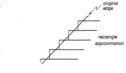
the MOS capacitance model shown in figure 24. Table 21 indicates how the capacitances are incorrectly estimated by the rectangular transistor. The total gate capacitance-a function of transistor area-is underestimated by 25%. The transistor capacitance problem is solved by adding other capacitive circuit elements. One of the solutions presented in figure 2-5 has two linear capacitors that correct for the total gate capacitance and the extrinsic gate-to-drain capacitance; the other solution has an "os capacitor" that corrects for the same capacitances, and includes a more accurate modelling of transistor channel charge. Either of these solutions can be included in standard extraction models of EXCL. The overestimated, extrinsic gate-to-source capacitance could be corrected with a negative capacitance. Since this element is unavailable in SPICE, it is best ignored.
T
L L/2 -1V - L/2 LeFigu re 2-3: Top view example of non-rectangular transistor.
19
X Xdj A Xd
aI
I I intrinsic art Ilf~t~*a~e I , I Gate _.- i "BDj'l ... I '. .. ''~ I.... .,I,.
I ... ODrain substrateFigure 2-4: MOS capacitance model.
Gate 1.5L Xd =... Source.e j~ [
OX
Drain Length = L Width = 1.5L Source-m Length = L Width = 1.5L (a) Length = 0.75L Width = 0.67L (b)Figure 2-5: Modelling corrections for non-rectangular transistor.
(a) Linear capacitors for total gate capacitance and
gate-to-drain capacitance guarantee a correct loading on the gate
node. (b) To approximate channel capacitance effects, an MOS
capacitor is added. 20 Gate 0.5 L 2 Cox rain Source CBe II I ... _ ..r I ---- -- c .__
r1
:(s$- GasI
I
I
cani C11. IdI
Cgate CGS. e Actual L X 1.5L rectangular Solution (a) Solution (b) 2 (L2CX ) 1.5 (L2CoX) 2 (L2CX) 2 (L2Cox) 1 (L xd Cox) 1.5 (L xd COX) 1.5 (L xd COx) 1.5 (L xd CoX) 3 (L xd Cox) 1.5 (L d COX) 3 (L xd COX) 3 (L xd COX)
Table 2-1: Capacitance values for non.rectangular transistor
2The value of Cqate includes all capacitance associated with the channel. This includes the voltage dependent CGD
i'
C CDi' and ateBS GS. i Bi BS~j'
21
----
2.4 Interconnection Capacitance Modelling
Two electrical parameters, resistance and capacitance, are extracted from layouts. To date, capacitance has been the more important for calculating circuit speed. Capacitive loading from interconnections frequently exceeds the capacitive loading from transistor gates.
2.4.1 Ground Capacitance
The total capacitance around a conductor is broken into the three components shown in figure 2-6. Inter-nodal capacitance forms between two conductors. The other two capacitances, edge and bottom capacitance, connect between the conductor and substrate. Since the substrate voltage remains fixed, these two capacitors are effectively "grounded"; the sum of edge and bottom capacitance is, therefore, known as ground capacitance. The dividing line between edge and bottom capacitor regions s only loosely defined by the plane extending straight down from the conductor edge. For a tighter definition, bottom capacitance is the portion of ground capacitance that is a function of conductor area (parallel to the substrate), and edge capacitance is the portion of ground capacitance that is a function of conductor perimeter. One can obtain good measurements for edge and ground capacitance with carefully selected test structures. One test structure has a very large circular conductor region. From this structure one measure mostly bottom capacitance. The other test structure has the same conductor surface area, but is arranged as a mesh of narrow conductor strips. The perimeter capacitance. which is no longer negligible, is calculated by subtracting the area related capacitance of the first test structure from the total measured capacitance of the second test structure.
Cinter-nodal
Conductor 1 Conductor
bottom edge
/ / / / / / substrate / / / / /);~
Figu re 2-6: Capacitance types for interconnections.
Each conductor layer has a different capacitance per unit dimension. In our typical NMOS
22
process, diffusion has the largest capacitance because of its proximity to the substrate; metal has the least. Table 2-2 gives some sample capacitance constants for the NMOS process. While metal and polysilicon capacitances are linear, the ground capacitance for diffusion is not. Diffusion capacitance effects arise from the voltage-dependent; space-char.e layer formed by the back-biased
p-n junction region under the diffused conductor. The junction capacitance as a function of junction
voltage, VD8, is
1- 08
(Ps
The process dependent parameters-zero-bias junction capacitance, C, bulk potential, (qB' and junction grading coefficient, w-are extracted during model parameter extraction. Only the layout dependent Area parameter comes from circuit extraction. The voltage-dependent capacitance value must be calculated in the circuit simulator, since V is a function of the simulation. In the circuit simulators, a back-biased diode properly models the voltage-dependent diffusion capacitance described in the above equation. Generally, two parallel, back-biased diodes are needed: one for diffusion bottom capacitance, the other for diffusion edge (or sidewall) capacitance. We can see that capacitance modelling with back-biased diodes requires two circuit parameters, Area and
Perimeter, and five model parameters, C w, Cjosw, wsw (the sw subscript is for "sidewall"
parameters), and qp8.3 Standard EXCL extraction models provide a switch that allows the user to
enable either an extraction model with accurate diode capacitance modelling or an extraction model with approximate linear capacitance modelling.
2.4.2 Inter-Nodal Capacitance
We have seen in figure 2-6 that the inter-nodal or coupling capacitance lies between two IC conductors. The two conductors can be on any pair of conductors and can have many orientations between them. Particularly strong capacitive coupling exists between overlapping conductors (such as metal over polysilicon), or between long stretches of parallel conductors. However, the extractor should be prepared for any conductor orientation. Since silicon dioxide separates all conductors, inter-nodal capacitors are linear. The only exception to this is between diffused conductors, where inter-nodal capacitance is minimal.
3
These model parameters are exactly the values included in the spice MOSFET model parameters, since SPICE includes diffusion capacitance if source or drain dimensions are specified.
23
Capacitance Cbottom C edge Cbottom C edge Cbottom C edge inter-nodal Cinter-fl odal diffusion, substrate diffusion, substrate polysilicon, substrate polysilicon, substrate metal, substrate metal, substrate diffusion. metal polysilicon, metal 1.25 X 10⁻⁴ pF / m2 3.5 X 10 4 pF / m 0.50 X 10⁻⁴ pF / m2 0.40 X 10⁻⁴ pF /m 0.25 X 10⁻⁴ pF/ m 2 0.40 X 10 -4 pF/ m 0.25 X 0.30 X 10-4 pF /m 2 10-4 pF / im2
Table 2-2: Sample capacitance constants for NMOS process
Con< g1 :tor 2 r _'g2
I
Figu re 2-7: Coupling capacitance between two nodes.
Inter-nodal capacitance values are used for circuit noise and speed analyses. When two nodes are coupled with an inter-nodal capacitance, Cc, as shown in figure 2-7, a change on one node
induces a voltage on the coupled node. In IC's, the induced voltage is coupling "noise". If the conductor 1 voltage changes by AV1, the induced voltage change on conductor two is
Cc
AV2 = AV1 C C 2' (2.1)
For digital IC designs, we can determine the maximum induced noise on conductor 2 by assuming a maximum voltage change on conductor 1. The maximum A V equals the difference between the high
24 Layer pair
Cc
and low logic voltages, Vign, - V w. If we are only interested in noise values greater than a minimum,
1AV.min 2 then using equation (2.1), we know that the following condition must hold:
A V
C > - (Cc + C2.in = Cg)* (2.2)
high low
We can effectively compute y by knowing the noise immunity characteristics of the logic circuits. A large number of the coupling capacitances in an LSI circuit fail the condition of equation (2.2), for potentially every node pair has some inter-nodal coupling. An extraction model that recognizes the condition, will be vastly more efficient. Inter-nodal capacitance effects speed analysis only by contributing its capacitance to a node's total capacitance. Activating the condition of equation (2.2) interjects a maximum error of y into the speed calculations.
2.5 Interconnection Resistance
Due to the uniform thickness and resistivity of integrated circuit conductors, the resistance problem is usually a two-dimensional, geometric one. In the well-known resistance equation,
R = (p Length) / (Width Thickness),
the known conductor thickness and material resistivity combine to give a new parameter, sheet
resistance or Pst, = p/Thickness. Resistance is now described by
R = (pa, Length) / (Width Thickness).
The dimension of psh is ohms, but it is typical to refer to the dimension as ohms per square (/[), since the ratio Length/Width gives the number of end-to-end "squares" for a conductor. Table 2-3 lists some sample sheet resistances for the NMOS process.
Conducting Layer Sheet Resistance
diffusion 12 02/1
polysilicon 25 Q2/O
metal 0.03 /1
Table 2-3: Sample sheet resistances for NMOS process
The resistance of an interconnection is calculated between different connections (contact
25
-cuts, transistor terminals, etc.). Chapter 3 gives a complete list of connection types. Some connections are single points, but the more interesting types extend over a large area; most notable in this category is the transistor channel to diffusion conductor connection. Usually, the resistivity on one side of the connection (channel) is much larger. than the. resistivity on the other (diffusion). In such cases, the tangential resistance is unimportant on the high-impedance side and important on the low-impedance side. Assuming a uniform voltage on the connection, the tangential resistance is modelled adequately when the full connection region is present on the high-impedance side. On the low-impedance side, however, separate connections are needed to account for tangential resistance (see figure 2-8).
low-impedance material
high-impedance material
Figure 28: Connections for modelling tangential resistance.
2.6 Modelling Distributed RC's
Both the resistance and capacitance effects distribute over the length of an IC interconnection. While some simulators can estimate delays directly for distributed RC lines [1 1], most simulators cannot. For such simulators, an extractor must generate an equivalent resistor and capacitor network with discrete nodes and elements. In EXCL, the resistance and capacitance extractors combine to model distributed RC's with an n-stage n-ladder network, as shown in figure 2-9. The total line resistance and capacitance are denoted by R and C, respectively. In addition to R and C, IC interconnections usually have a discrete drive resistance, RT, and a discrete load capacitance, CT, connected at opposite ends of the interconnection. RTand CT are shown for the one-stage nr-ladder.
As the number of 7-ladder stages increases, the modelling becomes more accurate. EXCL always breaks a resistive line and inserts a node at an interconnection branch, but to guarantee a certain modelling accuracy, long interconnections without branches may need added nodes to increase the number of ladder stages. For each node pair of the ?r-ladder network, EXCL inserts the whole, extracted resistance between the nodes and divides equally the extracted capacitance from the physical region between the nodes.
26 I _ _ _ _ I _ 1VV11 - -- %N I 1. - 1 . er n n atfl n
-""""
I
i
RT R/2 R/2
IC2
]
7C2
IT
1'4
7c2
'4
1-stage with drive resistor 2-stage
and load capacitor
R/3 R/3 R/3
IC16
jC/3
7C/3
7C6
3-stage
Figure 2-9: Pi-ladder networks for approximating distributed RC lines
The ladder network does not model the interconnection exactly, and how close the network approximates the actual behavior is discussed by Sakurai [12]. Appendix A calls upon these results and develops a criterion for the number of r-ladder stages needed. The criterion guarantees that the ladder network step response time does not vary by more than Ata.9from the true distributed RC step
response time. The time considered here measures the delay for voltage at the end opposite the step source to reach 90% of its final value.
2.7 Modelling Fabrication Degradations
The true physical regions on an IC differ in detail from the regions of a mask description. Errors with photolithography may cause real objects to expand or shrink from the mask specifications, or errors with mask alignment may cause an overall offset between two or more mask layers. These errors may alter interconnection resistance, inter-nodal capacitance, and even transistor size by a noticeable amount. To model the true behavior of the IC, the extraction model should simulate these anomalies by translating or expanding (shrinking) all rectangles of a layer by equal amounts.
27
CHAPTER THREE
Connectivity Extraction Algorithms
The connectivity extractor is divided into four subprograms. CIFPARSE and SORTREC execute first during an extraction and preprocess the geometric IC mask data. CONNECT, the third and main subprogram, converts geometric mask information into an internal circuit representation. Lastly, the fourth subprogram, FORMAT, converts the internal circuit representation into the appropriate output network format. The algorithms of each subprogram that pertain to extracting connectivity information from a layout are described in detail in this chapter.
3.1 Decomposition of Mask Geometries
The first subprogram, CIFPARSE, parses the geometric mask description provided by the user.
The most common and universal source is a Caltech Intermediate Form (CIF) [6] file. A CIF file is a collection of symbols describing IC geometric layouts. A symbol may contain mask objects such as rectangles, wires, polygons, point names, etc., each tagged with its mask layer. A symbol may also contain symbol calls to other, previously defined symbols.
CIFPARSE fully instantiates the geometric mask description into each of its component boxes and named points. Interiors of Boxes define the areas of interest for a given mask layer. A box is described by four integers representing the minimum and maximum x and y coordinates, and by one character representing the mask layer. A named point given by the user tags a mask region with a meaningful name; it is primarily used to tag a name to an electrical node. A named point is described by a character string for the name, and by an x and y coordinate and mask layer which locate the box region. After instantiation, these are the only geometric object types used by EXCL.
During the CIF instantiation process, all wires and polygons must be converted to an equivalent set of orthogonal rectangles, and all symbol calls must be replaced by the actual mask objects contained in the called symbol. Only named points from the top-level CIF symbol are retained to avoid
name conflicts arising from multiple calls to lower-level CIF symbols. Thus, after expansion the resulting data structure contains a "smashed" set of all boxes describing the layout and a set of named points from the top-level CIF symbol.
By instantiating the entire layout, we note that the layout hierarchy is lost, resulting in wasteful, repeated extractions of cell layouts which are replicated. A "hierarchical extractor"-that is an extractor that recognizes cell replications, and extracts the layout only once--would not only save extraction time, but could also pass the layout hierarchy through to the circuit network. The problem with this approach is that typically no restrictions are placed on the cell's layout boundary, thus allowing arbitrary overlaps of cells. (Allowing no overlaps, on the other hand, is too restrictive.) An erroneous overlap of cells could alter the intended network into something quite different. This IC design disaster must be detected by the extractor. Clearly, when a general hierarchical extractor looks for repeated cells, it must also examine the overlaps of other cells for each replication. This adds considerably to the extractor's execution time and complexity. A better approach is to support the layout and circuit hierarchy in a system at a higher level. Regulating and checking cell overlaps would be carried out in the higher-level system.
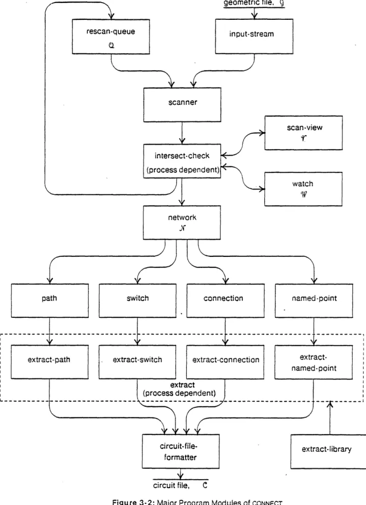
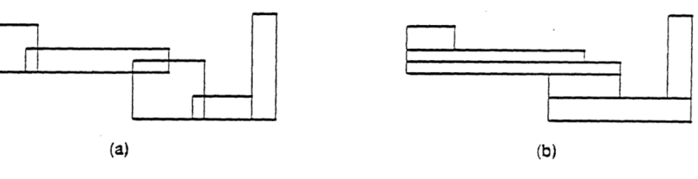
A second problem with converting the mask data to boxes is that of non-orthogonal line definitions. Handling non-orthogonal geometries properly necessitates additional complexity in the geometric data structures and procedures-complexity that has questionable value when considering the great infrequency of orthogonal geometries in IC layouts. In an alternate approach, a non-orthogonal geometry is converted into a set of smaller, non-orthogonal rectangles that approximate the original geometry as figure 3-i demonstrates. Geometric computations are affected as follows:
1. Calculations of area are no different than the actual values.
2. Calculated perimeter values are larger than the real values due to the staircase effect of the approximating rectangles.
3. Resistance calculations may be different. Non-orthogonal geometries always use general calculation methods. We will see in the next chapter that such methods divide the geometry into a square grid. If the staircase dimensions are small en-ough to match the grid spacing, resistivity calculations are not effected.
29
nriainal ,- .. ..
edge
,ctangle proximation
Figu re 3-1: Approximation for shapes with non-orthogonal edges
3.2 Sort by Maximum Y
In preparation for the scanning process of CONNECT, the second subprogram, SORTREC, sorts the
geometrical objects from maximum y coordinate to minimum y coordinate. A box's y coordinate is considered as the top of the rectangle. If one covered a plot of the layout with a sheet of paper and slowly pulled it down, the order of appearance of objects has the same ordering that results from
SORTREC.
3.3 Scan of Geometrical Objects
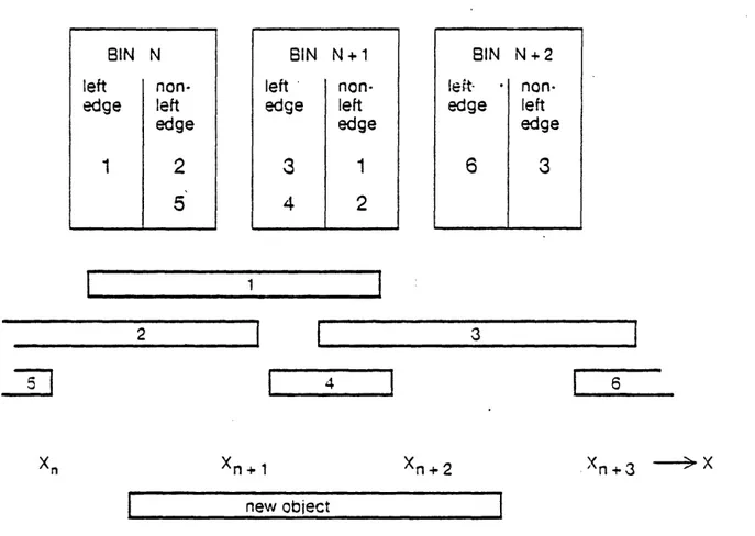
Once the entire layout has been decomposed into sorted mask objects, the next process is to locate the regions of relevant circuit elements defined by rectangle overlaps and to group together rectangles that are connected. This is the job of the third and major subprogram of the connectivity extractor. Figure 3-2 charts the major modules of the third subprogram. Each box represents (1) a collection of one or more procedures, and (2) in many cases, a data type upon which the procedures operate. The lines show the directions of information flow.
Basically, this subprogram, examines the mask objects sequentially from the geometric input file, . When an object is examined, relevant intersections with other mask objects in a "scan-view set", , are located and remembered. Then, the newly examined object is added to set rand the cycle is repeated with the next mask object from the input file. This can be a costly portion of connectivity
30
geometric file, (j rescan-queue f2,
\
scannerI1
_-_ _
connection extract-connection-I;
extract (process dependent) circuit-file- | formatter act-I-point7-
--ract-library circuit file, CFigure 3-2: Major Program Modules of CONNECT
31 intersect-check (process dependent) scan-view watch W network ... path switch
1---r u---___. ~~~~~~~ extrac I , II L - - - - -named-point extract-switch extr, named input-stream ]1 E II = . II_ _ _ __ I I i~~~~~
I
L ii I i II
, W~~~~~~~~ l .I
.I
.(--IIPI^----·---··- .11·_-11 -·1__11__ - ^-II1II__1Y·-·lll-l.__l 11 ---1I---I·_-·--I-I-··-C --LILI----L-·II-- ·-L--·--_l
1L
I
J'
I \1L ;t-path___1)
__
extraction if the mask object examination is done in a random order. The set i'continues to grow with each new object, and the complexity increases as the square of the number of rectangles.
3.3.1 Reducing the Vertical Search
The scanning process used by EXCL and other extractors 2] reduces execution time. A horizontal scan-line begins at the top of the layout. As the sorted mask objects are examined, the scan-line is always defined as the top edge of the mask object. Clearly, from the nature of the sort described in the previous section. the scan-line always moves downward. With the sorted scan, mask object intersection checks, need to be done only with rectangles still lying in the range of the scan-line. Thus, when the scan-line moves below a mask object in the "scan-view set", i. it is removed from further intersection checks. The execution time for this algorithm depends upon the number of objects at any given scan-line. and thus, roughly upon the width of the layout. For a square layout, the scanning process has a computation complexity approximately of order N'Log2N for N mask
objects.
3.3.2 Reducing the Horizontal Search
The scanning process narrows the search for intersecting rectangles to the approximate vertical coordinate. Narrowing the search along the horizontal coordinate results in a further reduction of computation complexity [13, 14]. One can do this by placing objects from the set f into horizontal bins. A bin contains all mask objects of S'which lie between two fixed horizontal coordinates, xnand
xn + ' Thus, each new mask object needs to be checked against only those objects in bins which fall in the same x-coordinate range as the new object.
The procedure is complicated slightly since the objects may span more than one bin as shown in figure 3-3. The objects within a bin are further subdivided into two columns:
1. The objects whose left edges are in the range of that bin are placed in the left edge column,
2. all other objects are placed in the non-left edge column.
When the "new object" is checked for intersections, we wish to check all mask objects from the bins which lie in its xcoordinate range, but only once for each object. The objects in both columns are checked from the bin at the left edge of the new object (bin N in figure 3-3), while only the objects in the left-edge column are checked in the remaining bins (bins N + 1 and N + 2). For the example in
32
I 1 !
2
I1~~
3i 4 1
Xn Xn+l1 Xn+2 Xn+3 > X
new object
Figure 3-3: Bin Placement of Mask Objects
Only the x-coordinates of the mask objects are shown; all objects intersect with the scan-line defined by the y-coordinate of the new object.
figure 3-3, mask objects 1 and 2 are checked only at bin N, not bin N + 1. Note also that the objects checked from bin N + 1 (mask objects 3 and 4) need no further x-coordinate intersection check, but that objects from the bins at the left or right edge of the new mask object (all mask objects except 3 and 4) must be checked further, for some of them may not actually intersect (as in the case of mask objects 5 and 6). 33 BIN N left non-edge left edge 1 2
5
BIN N+1 left ' non-edge left edge3
1
4 2 BIN N+2 left- · non-edge left edge 6 3 _~~~~~~~~~~~~~~I [11111^11·1---_1 1_--_1 1 --1_111^_-1-- C_^141- ·I l1 ^--_IIIII ·l-LI I-__---·---- 1 1I··_I- .---·IXIIII Il II _· - _ _ I
3.3.3 Rescan Queue
Although coordinate information below the scan-line is known during the examination of a rectangle, care must be taken to assume nothing about the geometries or connectivity below the scan-line. In some cases, new rectangles are defined which lie below the scan-line and thus should be reinserted into the sorted input stream to be examined at a later time. Such rectangles are inserted into the rescan-queue, Q. Rectangles in the rescan-queue are treated as though they are merged back into the geometric input stream, . To demonstrate how the rescan-queue might be used, consider the layout shown in figure 3-4.
I
nOcly5lIcon L -____
Udtfusn
7"'
Diffusion path ends here.
-...-, scan-line
\ A new 'channel' object
- and 'diffusion' object are
queued.
Figure 3-4: Scanning process of a Mos transistor layout
When the diffusion rectangle is first encountered, it is treated as a single rectangle. It is not until later, when the polysilicon rectangle is examined, that the extractor knows differently. The original diffusion rectangle becomes two diffusion rectangles (each a different node) and one "channel" rectangle. The extractor removes the original rectangle and replaces it by three rectangles: (1) the upper diffusion rectangle is added to the node of the original rectangle as though it has already been examined, (2) the channel rectangle and (3) the lower diffusion rectangle are added to Q., since they are on or below the scan-line. Details. of the operation on diffusion and polysilicon rectangles will be discussed the next section.
Procedure SCANNER demonstrates the main points presented in this section. INTERSECT-CHECK and NETWORK-CLEAN will be discussed later. (In the notation used here, a box, C3, precedes mask.
object variables, and underlined identifiers are constants.) 34
procedure SCANNER (): begin X,- empty network; -'emotv-aueue; D'- emot.-set; ;' - empty-watch;
next-clean - layout-top - clean-interval;
for each Cr E ( do
rec-scan-line - Cr.scan-line;
while QUEUEPEEK(Q.).scan-liFe > rec-scan-line do
[Is- OQUEUE-NEXT(C);
INTERSECT-CHECK(CS, X C, 'a, ,); end
INTERSECT-CHECK(Ilr, a, W, j);
if rec-scan-line < next-clean then
NETWORK-CLEAN(,, rec-scan-line, C);
next-clean - rec-scan-line - clean-interval;
end end for each Cls Ef Q do INTERSECT-CHECK(CS, Q, , , ', end NETWORK-CLEAN(.J, layout-bottom, C): retu rn(C) end
3.4 Geometrical Object Intersection
Up to this point, the program has made no distinction between the different layers of the mask objects. All operations have been independent of extraction-model or IC fabrication technology. This
section discusses the procedure INTERSECT-CHECK, a single procedure where all process-dependent,
geometric operations are defined. For instance, this procedure contains the rules governing which overlapping layers define a transistor, which rectangle combinations define a contact, and which rectangle groups define an interconnecting wire. It is one of the two extraction model dependent procedures.
INTERSECT-CHECK is called for each mask object that is examined during the scanning process. With each examined mask object, r, it updates the data structures by:
1. locating relevant intersections between r and other mask objects included in the "scan-view set", rc
35
-2. adding new mask objects appearing on or below the scan-line to the rescain-queue. (sect. 3.3.3),
3. adding new network information to T. and 4. placing r in the "scan-view set", 't
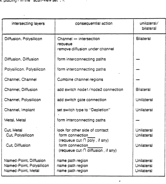
Table 3-1: Intersection checks for example NMCS process
To introduce INTERSECT-CHECK, the example NMOS process is used. Table 3-1 lists all of the relevant intersections for the NCS process. The second column lists the actions taken by INTERSECT.CHECK when an intersection is located, while the third column states whether the
36
intersecting layers consequential action unilateral/
bilateral
Diffusion, Polysilicon Channel - intersection Bilateral
requeue
remove diffusion under channel Diffusion, Diffusion form interconnecting paths Polysilicon. Polysilicon form interconnecting paths
Channel, Channel Combine channel regions
Channel, Diffusion add switch nodel /node2 connection Bilateral
Channel, Polysilicon add switch gate connection Unilateral
Channel, Implant set switch type to "Oepletion" Unilateral
Metal, Metal form interconnecting paths
Cut, Metal look for other side of contact Unilateral
Cut, Polysilicon form connection Unilateral
(requeue cut n poly, if any)
Cut, Diffusion form connection Unilateral
(requeue cut n diffusion, if any)
Named-Point, Diffusion name path region Unilateral
Named-Point, Polysilicon name path region Unilateral
Named-Point, Metal name path region Unilateral
--intersection needs to be checked in one direction or both. A bilateral intersection check is one
that must be made when either the first layer or the second layer is examined. Figure 3-5(a) shows two configurations for the bilateral intersection between Diffusion and Polysilicon. The intersection occurs in one case, while examining Diffusion, and in the other case, while examining
Polysilicon, The Diffusion- Polysilicon intersection demonstrates a typical bilateral intersection-the two layers cross, each extending outward from intersection-the intersection. A unilateral intersection check is one that needs to be made only when examining a rectangle of one of the layers-in the example, the first layer listed in the table. It is typical of unilateral intersections for the region of one layer to completely enclose the region of the other. Figure 3-5(b) shows a unilateral intersection between Cut and Metal. For the most part, the type of intersection is determined by the process' design rules. .-I I I I II Il L-- r- - - - -I Metal 1 scan-line I Ilu10 - --- ---. I I I I Iocilysificon I I I I diffusion
I---
Pa"Alcn . u I I-1
I I,,,,, (a) (b)Figu re 3- 5: Types of intersections
(a) Bilateral intersections, Diffusion
n
Polysilicon, and (b)unilateral intersection,
cut
n Metal.The distinction between bilateral and unilateral intersection checks has two consequences when writing the connectivity extractor. First, NTESECT-CHECK must have the ability to detect bilateral intersections from both directions, i.e., when examining either layer type. Secondly,.the unilateral
intersections of a process dictate the layer ordering or examining mask objects that sort to the same
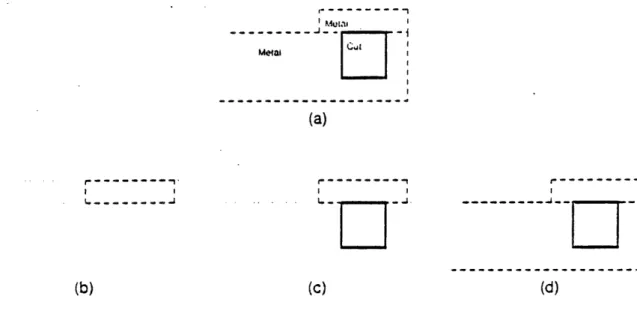
scan-line. If two mask objects which form a unilateral intersection are scanned at the same scan-line, then the object which does not activate the intersection check must be scanned first. Figure 3-6 shows how a contact cut might be missed if this rderig is not observed, and the Metal rectangle is examined last.
'- -- -- r - -' i M'I Metal l i (a)Mull~~~~~~ (a) . . . . . L. C (b) (c) I I - - - -- -)J__ _ ---(d)
Figure 3-6: A missed Metal-Cut intersection
(a) Original layout. The upper metal rectangle is examined (b). Then, when the scan-line moves down to the other boxes, the cut rectangle is examined next (c), and no intersection with
metal is found. When the metal rectangle is examined, no
intersection check with cut is made.
The complete INTERSECT-CHECK algorithm for the NMOS process is shown below. Procedures involving the network, ,X, will be discussed later. For clarity, variable names preceded by a box, C, refer to mask-object variables. Constant identifiers are underlined.
38
T-.. I ---
I,,,-{INTERSECT-CHECK for NMOS process. Inter-nodal capacitance windows are not located.)
procedure INTERSECT-CHECK (Or, QU.V,1V, N):
begin
case Or.layer of diffusion:
begin
(locate transistor regions)
for each Polysilicon intersection, OCp, in do
Ochannel - Cr n rp; QUEUE.AOO(, lchannel); Cdiffusion-fragmei7ts - d n channel; QUEUE-AOD((R, Cdiffusion-fragments); return; end diff-path - NEW-NETWCRK.PATH(.W", r);
(locate other path rectangles)
for each Diffusion intersection, Cd. and its path, p, in ( do
COMBItIE.NETWORK-PATHS(.'( p, diff-path);
end
(locate source or drain intersections)
for each Channel intersection, Cc, and its switch, s, in (l do
AOO-SOURCE/ORAIN(X,, , diff-path);
end
SCAN-VIEW-AOO(Ql, Or, diff-path);
end polysilicon:
begin
poly-path - NEN-NETNORK-PATH(J, Cfr);
for each Diffusion intersection, Cd, and its path, p, in a do
REMOVE-FRCM-PATH(JX, , Cd);
{locate transistors}
Ochannel i- ar a Cd; QUEUE-AOO(, Cchannel);
Cupper-d-fragment, Clower-d-fragments C- d n Ochannel ;
AOODD-TO-PATH@(, upper-d-fragment);
QUEUE-AODO(Q, Clower-d-fragments);
end
{locate other path rectangles}
for each Polysilicon intersection, CIp, and its path, p, in Q. do
CCMBINE.NETWORK-PATHS(.;, p, poly-path);
end
SCAN-VIEW-ADO(, Cr, poly-path);
end
39