HAL Id: hal-02324437
https://hal.archives-ouvertes.fr/hal-02324437
Submitted on 1 Nov 2019
HAL is a multi-disciplinary open access
archive for the deposit and dissemination of
sci-entific research documents, whether they are
pub-lished or not. The documents may come from
teaching and research institutions in France or
abroad, or from public or private research centers.
L’archive ouverte pluridisciplinaire HAL, est
destinée au dépôt et à la diffusion de documents
scientifiques de niveau recherche, publiés ou non,
émanant des établissements d’enseignement et de
recherche français ou étrangers, des laboratoires
publics ou privés.
Interface tailoring for charge injection mitigation in
insulators: Different principles and achievements
G. Teyssedre, S. Li, K Makasheva, N. Zhao, Christian Laurent
To cite this version:
G. Teyssedre, S. Li, K Makasheva, N. Zhao, Christian Laurent. Interface tailoring for charge injection
mitigation in insulators: Different principles and achievements. 2018 12th International Conference on
the Properties and Applications of Dielectric Materials (ICPADM), May 2018, Xi’an, China. pp.17-21,
�10.1109/ICPADM.2018.8401277�. �hal-02324437�
TABLE 1.
PRINCIPLE OF THE DIFFERENT METHODS ADDRESSED
Treatment Process outline Reasoning Grafting of
polar groups
Chemical grafting of polar atoms at the LDPE surface by exposure to F2/O2 gas mixture.
Polar groups are likely to produce deep traps for electrical charges
Thick nanocomposite layer
Interposition of a ≈30µm thick nano-composite made of BaTiO3 or TiO2 NPs and LDPE matrix by hot pressing
Charge stabilization owing to the high permittivity / high polarizability of NPs Thin nanocomposite layer Thin organosilicon dielectric layer deposition by plasma process incorporating a plane of Ag-NPs at controlled distance from the surface
Silver NPs owing to their ability to store positive or negative charges would act as deep traps for electrical charges
Interface Tailoring for Charge Injection Mitigation in
Insulators: Different Principles and Achievements
G. Teyssedre
1*, S.T. Li
2, K. Makasheva
1, N. Zhao
2, C. Laurent
11 Laplace, Université de Toulouse, CNRS, UPS, INPT, 118 route de Narbonne, F-31062 Toulouse Cedex 9, France; 2 SKLEIPE, School of Electrical Engineering, Xi’an Jiaotong University, Xi'an, Shaanxi, 710049, China
Abstract- Charge build-up in bulk insulation is one of the issues met in the development of materials for HVDC technologies. Progresses have been done for improving polymeric insulators, limiting charge build-up due to intrinsic processes. But margins of progress seem to be available by acting on the mitigation of charger generation at interfaces provided processes at play are well understood. In this contribution, we investigated different routes for tailoring the interface between electrode and polyethylene material, based on chemical modification of the insulation or layer intercalation. Three processes were tested, going from grafting of polar groups, thick nanocomposite layer intercalation up to thin nanocomposite layer deposition. Depending on the process, charge injection control is achieved either for negative charges or for charges of both polarities. The process of charge injection control is discussed with reference to the chemical/physical modifications brought about by the different treatments. The results provide indication towards a strategy to control the charge injection in power cables and other electrical components.
I. INTRODUCTION
In the development of HVDC technologies, one needs to handle the major drawback of insulating materials, which is the accumulation of electrical charges forming internal space charge with possibly two major issues: (i)- the out-of-control of the internal electric field distribution initiating current runaway [1] and (ii)- cumulated molecular level damages extending or creating defects and leading ultimately to breakdown [2]. As regards Polyethylene, which is the main material used in the insulation of HV cables, the efforts are directed to the reduction of crosslinked by-products or even the replacement by thermoplastic polymers and/or nanocomposites [3,4] and more generally to the understanding of charge trapping processes in those materials.
At the same time, it is recognized that charge build up [5,6] and even conductivity measurement results [7,8] heavily depend on electrode conditions of samples and not only on bulk properties of insulations. The screening of insulation and semicon materials for HVDC cables was achieved resorting to space charge criteria, but without real insight into why couples of materials perform better than others [9].
To prevent space charge accumulation, one necessary route, not examined in depth by the scientific community to date, is to control the charge injection at the interfaces between the insulating material and the “electrodes” (metallic or semi-conducting). Relatively few studies focus on the tailoring of interface properties to change its characteristics in terms of charge trapping probably because in way the phenomena at
play are complex and not correctly described. Two families of processes have been envisaged, consisting either in the chemical modification of the polymeric insulator, by e.g. fluorination or plasma attack [10, 11], or in intercalating a new layer between the insulator and the electrodes.
Results presented in the present contribution were obtained in the frame of the InTail project jointly run by Laplace and Skleipe Labs, aiming at tailoring the interface of dielectrics for charge injection mitigation. Three routes have been followed and trends obtained for each of them are briefly described, more details being given in [12].
II. PROCESSES FOR INTERFACE MODIFICATION
Different interface modifications have been implemented to the same kind of insulation, being low density polyethylene -LDPE, so as to get simple response. LDPE substrates were press-molded into films of typically 300 µm thickness and 80 mm diameter.
Features of the implemented three surface modification processes are summarized in Table 1. Two of them consider the addition of an interface layer: As thick layer (10-100 µm) we used a nanocomposite with high permittivity nanoparticles and LDPE matrix. As thin layer (less than 100 nm), a silver nanoparticles-containing organosilicon layer was deposited by plasma process. The last method consists in chemically modifying the LDPE matrix by chemical attack leading to an intermediate thickness treated layer (2 µm). The methods have in common to target charge trapping at the interface: the field at the electrode would be reduced and so the injection current.
Fig. 2. Space charge density profiles of (a) reference LDPE at polarization E=50 kV/mm, (b) reference LDPE at depolarization after E=50 kV/mm, (c) oxy-fluorinated LDPE at polarization E=50 kV/mm and (d) oxy-fluorinated LDPE at depolarization after E=50 kV/mm.
0 100 200 300 400 500 -60 -40 -20 0 20 40 an od e (C/m 3) (C/m 3) (C/m 3) (d) (c) (b) Reference LDPE Polarization E =50 kV/mm (C/m 3) 2 s 10 s 5 min 10 min 20 min ca th od e (a) 0 100 200 300 400 500 -20 -15 -10 -5 0 5 10 Position (m) Reference LDPE Depolarization after E =50 kV/mm 5 s 60 s 150 s 300 s Position (m) 0 100 200 300 400 500 -60 -40 -20 0 20 40 Oxyfluorinated LDPE (O/F_30) Polarization E =50 kV/mm 2 s 10 s 5 min 10 min 20 min Position (m) 0 100 200 300 400 500 -20 -15 -10 -5 0 5 10 Oxyfluorinated LDPE (O/F_30) Depolarization after E =50 kV/mm 5 s 60 s 150 s 300 s Position (m)
Fig. 1. SEM cross-sections of: Left - oxy-fluorinated LDPE; Right - AgNPs-containing organosilicon layer deposit on LDPE substrate.
d=1.7µm
oxy-fluorination and of LDPE provided with silver nanoparticles-containing organosilicon layer.
Assessment of the efficiency in charge injection mitigation was achieved through a main means consisting in space charge measurements in all instances, using similar protocols. Pulsed Electroacoustic -PEA measurements were carried out at room temperature with relatively short charging time (typically 20 min) in order to analyze the earlier instants of charge injection into the materials, and applying fields in the range 10 to 50 kV/mm. This was complemented by physicochemical analyses adapted to the process considered.
III. RESULTS AND DISCUSSION
A. (Oxy-) Fluorination
Fluorination and oxy-fluorination introduce polar groups at the surface of the material, likely to stabilize charges. The process consists in exposing the polymeric material to F2
and/or O2 gas mixture with N2. It is one of the most effective
approaches to enhance the adhesion properties of polymers. Three process schemes: oxy-fluorination (labeled as O/F), fluorination (F) and oxy-fluorination followed by fluorination (O/F+F) were implemented for tailoring the LDPE interface. The treatment times were 30 or 60 min, the gas volume ratio were 1 part of F2 and/or O2 in 4 parts of N2 and the total
pressure was 110 to 150mbar. The temperature was 25°C. The thickness of the oxy-fluorinated/fluorinated layer varies from about 0.1 µm to several microns depending on process conditions.
Fig. 2 shows space charge profiles obtained for oxyfluorination of LDPE for 30 min as compared to bare LDPE. It can be seen that holes and electrons are injected into the reference LDPE, forming positive and negative homocharges in the vicinity of the injecting electrodes. After O/F treatment, only positive space charge can be observed in the sample, which indicates that electron injection is efficiently suppressed by oxy-fluorination but hole injection seems to be hardly influenced. The same qualitative features were observed for fluorination, with an amount of space charge less than by oxy-fluorination. The combination of O/F abnd F treatment further reduced it but the net space charge, as measured after 5s under volts off remains significantly higher than in bare LDPE, and the qualitative features are the same.
Interface tailoring processes with the three proposed schemes all have marked suppression effect on the electron injection even under mild process conditions regardless of the fluorination intensity and introduction of oxygen atom.
However, the hole injection cannot be suppressed by the tailoring methods and even increases with process duration and pressure increasing, resulting in an increase of the total space charge.
XPS analyses were carried out to evaluate chemical modifications. It appears that F-treatment leads to hydrogen abstraction and F grafting. In the O/F-process oxygen hinders fluorination, which has positive effect with moderating F-grafting, but there can be peroxy radical formation and more complex chemistry with interaction with moisture for example [13]. The impact of the process on the polarity of charges is worth discussing: three mechanisms can be influenced, namely modification of barrier to injection, change of transport properties in the bulk or deep trapping. At the difference of other surface modification processes, as oxy-fluorination is a chemical attack of the material made in a vessel, it is not easy to modify only one face of the samples to provide a guess of the mechanisms. The barrier to injection is probably not the leading factor as in general the injection of charges is not by a process over the barrier but rather by channel through the barrier and involvement of localized states, especially in the case where defects are created. Transport in the volume can be modified through free volume decrease due to the size of F-atoms and crosslinking. This would slow down the transport of electrons. So the injected electrons would be trapped in the surface layers. As fluorine has strong electron affinity, it can be anticipated that it efficiently stabilizes excess negative charges but tends to repulse positive ones. It appears therefore not straightforward to block positive charge generation by fluorination treatment.
B. Thick nanocomposite layer intercalation
Dispersion of nanoparticles (NPs) into polymer matrixes has proved to be very effective in suppressing space charge build-up, as e.g. nanometer-size fillers of silica (SiO2) [14] and
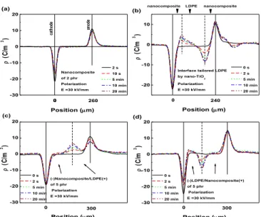
Fig. 3. Space charge density profiles of (a) single layer of NC; (b) LDPE with layers of NC on each face, (c) bilayer of NC/LDPE with anode on LDPE; (d) bilayer of LDPE/NC with anode on NC. NC is LDPE with 5 phr nano-TiO2 in all cases. Applied field E=30 kV/mm.
-30 -20 -10 0 10 20
nanocomposite LDPE nanocomposite
an od e (C/m 3) (C/m 3) (C/m 3) (d) (c) (b) Nanocomposite of 2 phr Polarization E =30 kV/mm (C/m 3) 2 s 10 s 5 min 10 min 20 min ca th od e (a) -20 -10 0 10 240 0
Interface tailored LDPE
by nano-TiO2 Polarization E =30 kV/mm 260 Position (m) 0 s 2 s 5 min 10 min 20 min Position (m) 0 -30 -20 -10 0 10 20 300 0 0 0 (-)Nanocomposite/LDPE(+) of 5 phr Polarization E =30 kV/mm 0 s 2 s 5 min 10 min 20 min Position (m) -30 -20 -10 0 10 20 (-)LDPE/Nanocomposite(+) of 5 phr Polarization E =30 kV/mm 0 300 0 s 2 s 5 min 10 min 20 min Position (m)
magnesium oxide (MgO) [3] into LDPE. Though the mechanisms behind these improvements are not completely clear at present, an interpretation based on deep trap formation at the interface between LDPE and MgO nanoparticles was put forward [15]. Our purpose in this work was to use a nanocomposite (NC) with NPs of high dielectric permittivity as a thick interface layer. The strategy is guided by a two-fold objective: first, owing to their high permittivity, particles would act as deep traps for charges. In the field of organic semiconductors, it is recognized that high-k dielectrics produce carrier localization enhancement and charge formation at the interface between the dielectric and semiconductor material [16]. Second, the interface layer would decrease the field in the higher permittivity part of the material, i.e. at the interface with electrodes, which is considered as constituting the weak region of insulators. So far scarce reports concern space charge of nanocomposite multilayers [17].
The sample processing conditions are available elsewhere [18]. Titanium oxide nanoparticles (nTiO2) with diameter
20±5 nm, surface-treated by silane, were dispersed into the LDPE in different concentrations in the range from 0.5 to 10 phr (parts per hundred parts of resin). The TiO2-LDPE
nanocomposite (NC) materials were press-molded into thin films of 60 µm thickness. Films were further co-pressed into bilayers or three-layer stacks of about 250 µm thickness, under a pressure of 10 MPa at 80 °C for 20 min.
The space charge profiles of the TiO2-LDPE NCs single
layers with different nanoparticle contents were measured by PEA method. As example, the results obtained for 5 phr TiO2
are shown in Fig. 3a. The positive and negative space charge formed in the bare LDPE, cf. Fig. 2a cannot be observed anymore, indicating that TiO2 nanoparticle doping can
effectively suppress both positive and negative space charge build-up, which is in good agreement with previous reports [19]. The electrical conductivity is substantially reduced, by a factor over 10 in the NCs compared to the LDPE.
Space charge profiles obtained on the LDPE film provided with NC layers with 5phr TiO2 are shown in Fig. 3b. It can be
seen that both negative and positive heterocharges are formed near the anode and cathode, respectively. In order to make clear the origin of these heterocharges, two-layer samples LDPE/NC were prepared by stacking thin films of LDPE and NC and using thicker NC layer (120 µm) in order to resolve features at the interfaces. The space charge characteristics of the bilayer samples are shown in Fig. 3c and 3d, where the NC is either at cathode or anode. A space charge region is formed at the LDPE/nanocomposite polymer interface in both cases, and coincide well with the space charge clouds of the interface tailored LDPE in Fig. 3b, showing that the heterocharges originate from dielectric/dielectric polymer interfaces. The sign of the charge is consistent with that predicted from Maxwell Wagner process [12].
Therefore, space charge in LDPE tailored with NCs is driven by two processes. The TiO2-LDPE NC as an intercalated layer
suppresses hole and electron injection from both electrodes due to its excellent charge suppressing ability shown in Fig. 3a. The ability mainly originates from the increase of trap amount
and trap level caused by TiO2 NPs. In addition the thick NC
layers introduce two dielectric/dielectric interfaces, on which an interface charge is formed, appearing as heterocharge owing to a lower conductivity in the NC layer than in LDPE. Definitely, the first process has positive effects for limiting space charge accumulation. The second one has as consequence to increase the electric field at both electrodes and may enhance charge injection, which goes against reducing charge accumulation in the LDPE. This should be avoided by choosing materials with proper conductivity and permittivity to reverse the sign of the interfacial charge.
C. Plasma-processed nanocomposite layer
One possible route for preventing charge build-up consists in forming deep traps at the interface in a way to permanently trap the injected charges. This would provide two effects: on one hand, the trapped charges would induce a counter field which will moderate the injecting field at the electrode thereby reducing further injection and on the other hand these charges would not be available anymore for transport. A rough estimation shows that, in order to reduce the field at the contact, typically by about 10 kV/mm as order of magnitude of applied field, a trap density of 6×1011 cm-2 is needed, representing an inter-particle distance of 13 nm if each particle holds one charge only. In order to do so, we have processed a thin dielectric layer containing a single layer of silver nanoparticles -AgNPs [20]. By their metallic nature, the AgNPs would stabilize the injected charges and the distance between the electrode and the plan of the silver nano-grains would allow an efficient capture of the injected carriers.
The nanocomposite layer used for tailoring LDPE interfaces consists of AgNPs/SiOxCy:H stack. The deposition was
performed in two-steps process: silver sputtering to obtain the single layer of AgNPs followed by plasma polymerization to create the dielectric embedding matrix. Tuning of the plasma
Fig. 4. Space charge density versus position of (a) reference LDPE at polarization E=50 kV/mm, (b) reference LDPE at depolarization after E=50 kV/mm, (c) two-face tailored with AgNPs/plasma polymer stack LDPE at polarization E= 50 kV/mm and (d) tailored LDPE at depolarization after E= 50 kV/mm. 0 100 200 300 400 -20 -10 0 10 anode 0s 5min 10min 20min 0s 5min 10min 20min ( C/ cm 3 ) Position (m) cathode Volt-on 0 100 200 300 400 -2 -1 0 1 2 Volt-off ( C/ cm 3) Position (m) cathode anode 0 100 200 300 400 -20 -10 0 10 Volt-on 0s 5min 10min 20min ( C/ cm 3 ) Position (m) cathode anode 0 100 200 300 400 -2 -1 0 1 2 (b) (a) Volt-off 0s 5min 10min 20min
Two-face tailored with S1 LDPE 50kV/mm Bare LDPE 50kV/mm ( C/ cm 3) Position (m) cathode anode (a) (b) (c) (d)
Fig. 5. Current-field plot obtained for reference LDPE and LDPE with tailored interfaces using SC electrodes. Data are relevant to charging current after 16 min of polarization.
10 100 10-9 10-8 10-7 10-6 b = 0.9 Bare LDPE
Two-face tailored with S1 LDPE
Curre nt de ns ity ( A/m 2 ) Vappl./d (kV/mm) a = 2.1
operating conditions, such as discharge power and sputtering time allows strict control over the size and density of the AgNPs in the dielectric matrix. The processed dielectric layer to cover the AgNPs is a plasma organosilicon deposit (SiOxCy:H) obtained in the same reactor with
argon-hexamethyldisiloxane mixture. The so-formed nanocomposite stack has 50 nm total thickness, cf. Fig. 1.
Either one or the two faces of the 300 µm thick LDPE sample were tailored with identical nanocomposite layers. Three values of the input power (40 to 80 W) and two values of the argon pressure (8.00 and 5.33 Pa) were used for AgNPs processing. Details on the structural characterization of the obtained nanocomposites and the relation between plasma parameters and AgNPs features are given elsewhere [20]. The size of particles could be tuned from less than 10 nm to more than 40 nm in diameter and the AgNPs could be ultimately coalesced. Considering a size of 15 nm for the AgNPs, which provided the best results in terms of space charge mitigation, the NC layer can be represented by a first region consisting of a plan of AgNPs embedded in organosilicon matrix of 35 nm in thickness, and a second one of only organosilicon layer with thickness estimated to 50 nm.
Fig.4 shows the space charge patterns obtained for bare LDPE and for LDPE with two-face tailored interfaces, both in volts-on and in volts-off for 50 kV/mm of applied field. In order to make the comparison independent from test electrodes, semicon layers were used on both faces of the samples. Prior to measurement, bare LDPE was submitted to the same vacuum conditioning as for the sample with processed nanocomposite layers in order to make the comparison with equal outgassing degree. As can be seen in the pictures, positive charges appear as the dominant carriers
in those conditions, consistently with experimental and modelling results reported previously [21]. Changing the polarity leads to nearly symmetrical space charge patterns, with again positive space charge region forming at the positive electrode and progressively extending to the bulk of the material. In case of tailored interfaces, the amount of space charge is greatly reduced, with virtually no charges being accumulated in the bulk and with field distribution exhibiting no evolution with charging time [20]. With using one-face tailored sample, it was confirmed that the treatment is efficient for both positive and negative charge injection. Already the organosilicon layer appears efficient in mitigating the space charge build-up. The introduction of AgNPs to form the stack strengthens the effect, provided large and isolated particles are settled at appropriate distance from the interface.
To further substantiate the results, we have plotted in Fig. 5 the current-voltage characteristics obtained at room temperature for bare LDPE and for two-face tailored LDPE. In both cases, the electrode in contact with the sample is a semiconducting material, i.e. the same configuration as for the space charge measurement results plotted in Fig. 4. As can be observed there is a substantial difference in the behavior of the two samples. First, a quantitative difference, with a drop of the apparent conductivity by about one decade in the sample with tailored interfaces, in the high field range. Second, there is a qualitative difference through a change in the slope of the current-voltage characteristic from 2 to almost 1, i.e. from what seems relevant to a space charge limited current to a behavior featuring ohmic conductivity. This appears consistent with the observed drastic reduction of charge injection.
IV. CONCLUSIONS
Briefly we can conclude the following about the efficiency of the three modification routes:
(i) We confirmed that TiO2 dispersion into LDPE leads to
substantial space charge reduction, in line with many of literature reports using insulating inorganic particles in general and TiO2 in specific. Interface tailoring by intercalating TiO2
-LDPE nanocomposite interface layer suppresses hole and electron injection because the trap amount and trap depth are
increased by TiO2 nanoparticle doping. However, at present,
the association of nanocomposites of the form used and LDPE leads to interface charge build-up appearing as heterocharge owing to the relative values of permittivity and conductivity in the intercalated layer and LDPE. Is not necessarily a reliable route as it will lead to field intensification into the LDPE layer. Changing the matrix is a track to investigate.
(ii) After treating the surface of LDPE by fluorination or
oxy-fluorination, electron injection appears fully suppressed even under weak process conditions regardless of the introduction of oxygen atom. However, it cannot suppress hole injection and even increases net positive charge build up under strong process conditions, resulting in the increase of the total space charge, presumably because the interface tailoring shallows hole traps. In addition, the introduction of O atoms hinders the fluorination reaction and enhances hole injection from the anode. Because of the activation of the surface, the O/F process should be rigorous control with avoiding interaction with moisture for example.
(iii) Thin plasma deposited layers containing metallic NPs
prevents very efficiently negative and positive charge build-up into LDPE. This is the first report in the literature on this aspect. The effect is explained by the trapping of charges on the particles and subsequent screening of the field at the interface with the electrode adjacent to the layer. AgNPs-containing nanocomposite is therefore considered as an efficient barrier for electron and hole injection.
Although charge injection control was investigated on laboratory structures, the work displays a panel of interface tailoring routes. Useful information is brought on process constrains, issues and merit for implementing interface modification in real systems. The process of changing the interface properties should of course be compatible with the production technology of the components. In the case of HVDC cable, surface chemical modification could be implemented during the extrusion process, as well as incorporating NPs, would it be carbon black (CB) particles close to the interface if their electronic properties provide similar effects as for AgNPs. Out of the cable application, tailoring interfacial electronic properties can be achieved by plasma deposition of thin nanostructured dielectrics. The versatility of the plasma process makes this technique applicable to different electric and electronic components.
ACKNOWLEDGMENT
This work was jointly supported by Agence Nationale de la Recherche in France, project ANR-InTail under Contract No. ANR-AA-PBLI-II-2011 and China National Funds for International (regional) projects of cooperation and exchange (Grant No. 51161130524).
REFERENCES
[1] Y. Zhang, J. Lewiner, C. Alquié and N. Hampton, "Evidence of strong correlation between space-charge buildup and breakdown in cable insulation", IEEE Trans. Dielectr. Electr. Insul, vol. 3, pp. 778–783, 1996. [2] G.C. Montanari, "Bringing an insulation to failure: the role of space charge", IEEE Trans. Dielectr. Electr. Insul., vol. 18, pp. 339–364, 2011.
[3] Y. Murakami, M. Nemoto, S. Okuzumi, S. Masuda, M. Nagao, N. Hozumi, Y. Sekiguchi and Y. Murata, "DC conduction and electrical breakdown of MgO/LDPE nanocomposite", IEEE Trans. Dielectr. Electr. Insul., vol. 15, pp. 33–39, 2008.
[4] I. Plesa, P.V. Notingher, S. Schlögl, C. Sumereder and M. Muhr, "Properties of polymer composites used in high-voltage applications", Polymers, vol. 8, p. 173 (pp. 1-63), 2016.
[5] G. Chen, Y. Tanaka, T. Takada and L. Zhong, "Effect of polyethylene interface on space charge formation," IEEE Trans. Dielectr. Electr. Insul., vol. 11, pp. 113–121, 2004.
[6] M. Taleb, G. Teyssèdre and S. Le Roy, "Role of the Interface on Charge Build-up in a Low-Density Polyethylene: Surface Roughness and Nature of the Electrode", Proc. IEEE Conf. Electr. Insul. Dielectr. Phenom. (CEIDP), pp. 112–115, 2009.
[7] M. Jeroense, M. Saltzer and H. Ghorbani, "Technical challenges linked to HVDC cable development", Revue Electricité Electronique, No. 4, pp. III–X, 2014.
[8] U.H. Nilsson, J. Andersson, V. Englund, V. Eriksson, P.O. Hagstrand and A. Smedberg, "The role and measurement of dc conductivity for HVDC cable insulation materials", Proc. IEEE Conf. Electr. Insul. Dielectr. Phenom. (CEIDP), pp. 31–34, 2015.
[9] D. Fabiani, G. C Montanari, C. Laurent, G. Teyssedre, P.H.F. Morshuis, R. Bodega, L.A. Dissado, A. Campus and U.H. Nilsson, "Polymeric HVDC cable design and space charge accumulation. Part 1: insulation/semicon interface", IEEE Electr. Insul. Mag., vol. 23-6, pp. 11–19, 2007
[10] Z. An, Q. Yang, C. Xie, Y. Jiang, F. Zheng and Y. Zhang, "Suppression effect of surface fluorination on charge injection into linear low density polyethylene", J. Appl. Phys., vol. 105, p. 064102, 2009.
[11] H. Hayashi, T. Nakano and Y. Ohki, "Effect of plasma surface modification on electrical conduction in polyethylene", Elect. Eng. Jpn., vol. 111, pp. 17–24, 1991.
[12] G. Teyssedre, S.T. Li, K. Makasheva, N. Zhao, L. Milliere and C. Laurent, "Interface tailoring for charge injection control in polyethylene", IEEE Trans. Dielectr. Electr. Insul., vol. 24, pp. 1319– 1330, 2017
[13] A.P. Kharitonov and L.N. Kharitonova, "Surface modification of polymers by direct fluorination: A convenient approach to improve commercial properties of polymeric articles," Pure Appl. Chem., vol. 81, pp. 451–471, 2009.
[14] X.Y. Huang, P.K. Jiang and Yi Yin, "Nanoparticle surface modification induced space charge suppression in linear low density polyethylene", Appl. Phys. Lett., vol. 95, p. 242905, 2009.
[15] T. Takada, Y. Hayase, Y. Tanaka and T. Okamoto, "Space charge trapping in electrical potential well caused by permanent and induced dipoles for LDPE/MgO nanocomposite", IEEE Trans. Dielectr. Electr. Insul., vol. 15, pp. 152–160, 2008.
[16] W. Xu, F. Wang, S.W. Rhee and S.M. Khaffaf, "Quasi-ordering in spontaneously associated surface dipoles: an intrinsic interfacial factor for high-k polymer insulated organic field-effect transistors", J. Mater. Chem., vol. 22, pp. 1482–1488, 2012.
[17] E. Kanegae, Y. Ohki, T. Tanaka and Y. Sekiguchi, "Space charge behavior in multi-layered dielectrics with LDPE and LDPE/MgO composites", Proc. IEEE Int’l. Conf. Solid Dielectr. (ICSD, Potsdam, Germany), pp.1–4, 2010.
[18] S.T. Li, N. Zhao, Y.J. Nie, X. Wang, G. Chen and G. Teyssedre, "Space charge characteristics of LDPE nanocomposite/LDPE insulation system", IEEE Trans. Dielectr. Electr. Insul., vol. 22, pp. 92–100, 2015. [19] R.J. Fleming, T. Pawlowski, A. Ammala, P.S. Casey and K.A.
Lawrence, "Electrical conductivity and space charge in LDPE containing TiO2 nanoparticles," IEEE Trans. Dielectr. Electr. Insul., vol. 12, pp. 745–753, 2005.
[20] L. Milliere, K. Makasheva, C. Laurent, B. Despax, L. Boudou and G. Teyssedre, "Silver nanoparticles as a key feature of a plasma polymer composite layer in mitigation of charge injection into polyethylene under DC stress", J. Phys. D, vol. 49, p. 015304, 2016.
[21] S. Le Roy, G. Teyssedre, C. Laurent, G.C. Montanari and F. Palmieri, "Description of charge transport in polyethylene using a fluid model with a constant mobility: fitting model and experiments", J. Phys. D, vol. 39, pp. 1427–1436, 2006.