HAL Id: hal-03162094
https://hal.archives-ouvertes.fr/hal-03162094
Submitted on 8 Mar 2021
HAL is a multi-disciplinary open access
archive for the deposit and dissemination of
sci-entific research documents, whether they are
pub-lished or not. The documents may come from
teaching and research institutions in France or
abroad, or from public or private research centers.
L’archive ouverte pluridisciplinaire HAL, est
destinée au dépôt et à la diffusion de documents
scientifiques de niveau recherche, publiés ou non,
émanant des établissements d’enseignement et de
recherche français ou étrangers, des laboratoires
publics ou privés.
Distributed under a Creative Commons Attribution - NonCommercial - ShareAlike| 4.0
International License
Broad Diversity of Near-Infrared Single-Photon
Emitters in Silicon
Alrik Durand, Yoann Baron, Walid Redjem, T. Herzig, A. Benali, S.
Pezzagna, J. Meijer, A. Yu. Kuznetsov, J.-M. Gérard, I. Robert-Philip, et al.
To cite this version:
Alrik Durand, Yoann Baron, Walid Redjem, T. Herzig, A. Benali, et al.. Broad Diversity of
Near-Infrared Single-Photon Emitters in Silicon. Physical Review Letters, American Physical Society, 2021,
126 (7), pp.083602. �10.1103/PhysRevLett.126.083602�. �hal-03162094�
Broad diversity of near-infrared single-photon emitters in silicon
A. Durand,1 Y. Baron,1 W. Redjem,1 T. Herzig,2 A. Benali,3 S. Pezzagna,2 J. Meijer,2 A. Yu. Kuznetsov,4
J.-M. G´erard,5 I. Robert-Philip,1 M. Abbarchi,3 V. Jacques,1 G. Cassabois,1 and A. Dr´eau1,⇤
1Laboratoire Charles Coulomb, Universit´e de Montpellier and CNRS, 34095 Montpellier, France
2Division of Applied Quantum Systems, Felix-Bloch Institute for Solid-State Physics,
University Leipzig, Linn´eestraße 5, 04103 Leipzig, Germany
3CNRS, Aix-Marseille Universit´e, Centrale Marseille, IM2NP,
UMR 7334, Campus de St. J´erˆome, 13397 Marseille, France
4Department of Physics, University of Oslo, NO-0316 Oslo, Norway
5Department of Physics, IRIG-PHELIQS, Univ. Grenoble Alpes and CEA, F-38000 Grenoble, France
We report the detection of individual emitters in silicon belonging to seven di↵erent families of optically-active point defects. These fluorescent centers are created by carbon implantation of a commercial silicon-on-insulator wafer usually employed for integrated photonics. Single photon emission is demonstrated over the [1.1,1.55]-µm range, spanning the O- and C-telecom bands. We analyse their photoluminescence spectrum, dipolar emission and optical relaxation dynamics at 10K. For a specific family, we show a constant emission intensity at saturation from 10K to temperatures well above the 77K-liquid nitrogen temperature. Given the advanced control over nanofabrication and integration in silicon, these novel artificial atoms are promising candidates for Si-based quantum technologies.
The boom of silicon in semiconductor technologies was closely tied to the ability to control its density of lattice defects [1]. After being regarded as detrimental to the crystal quality in the first half of the 20th century [2],
point defects have become an essential tool to tune the electrical properties of this semiconductor, leading to the development of a flourishing silicon industry [1]. At the turn of the 21st century, progress in Si-fabrication and
implantation processes has triggered a radical change by enabling the control of these defects at the single level [3]. This paradigm shift has brought silicon into the quantum age, where individual dopants are nowadays used as ro-bust quantum bits to encode and process quantum infor-mation [4]. These individual qubits can be efficiently con-trolled and detected by all-electrical means [4], but have the drawback of either being weakly coupled to light [5] or emitting in the mid-infrared range [6] unsuitable for op-tical fiber propagation. In order to isolate matter qubits that feature an optical interface enabling long-distance exchange of quantum information while benefiting from well-advanced silicon integrated photonics [7], one strat-egy is to investigate defects in silicon that are optically-active in the near-infrared telecom bands [8, 9].
Point defects emitting light exist in various semi-conductors [10–12]. While individual solid-state artifi-cial atoms have been observed in several wide bandgap semiconductors such as diamond [13, 14], silicon car-bide [15, 16] or hexagonal boron nitride [17], silicon is lagging behind [12]. The first optical detection of a single optically-active defect in silicon has only been reported recently [18] and reproduced in [19]. Besides this defect related to a carbon-complex called the G-center [20–22], we report here that silicon, despite its small bandgap, hosts a large variety of emitters that can be optically isolated at single scale. We identify six new families of
individual fluorescing defects in carbon-implanted silicon, that emit single photons in the near-infrared range cov-ering the O- and C-telecom bands. We investigate their photoluminescence spectra, dipolar emission and radia-tive recombination dynamics through lifetime measure-ments. At last, we demonstrate that G-centers have a constant emission intensity at saturation, from 10K to well above liquid-nitrogen temperatures.
The investigated sample comes from a commercial silicon-on-insulator (SOI) wafer (Soitec). The top 220-nm thick silicon layer was implanted with 36-keV carbon ions at a fluence of 5⇥ 1013cm 2. To heal the lattice
from damages generated during this process, the sam-ple underwent a subsequent flash annealing at 1050 C during 20 seconds. The experimental setup consists in a low-temperature scanning confocal microscope operating with above-bandgap optical excitation at 532 nm. The sample photoluminescence (PL) is collected by a high numerical aperture microscope objective (NA=0.85) and measured with fiber-coupled single-photon detectors fea-turing a detection efficiency of 10%. The optical detec-tion window was set to cover the near-infrared range from 1.1 µm to 1.55 µm. More details about the sample prepa-ration and optical setup can be found in [18].
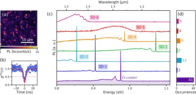
A PL image of the sample at 10K reveals a multi-tude of fluorescing spots (Fig. 1(a)). Analyzing their photon emission statistics with a Hanbury-Brown and Twiss setup indicates that all the isolated bright spots appear to be single emitters. Their autocorrelation func-tion g(2)(⌧ ) presents a clear antibunching that fulfills the
single-emitter condition: g(2)(0) < 0.5 [24], as displayed
on Fig. 1(b) (see SI). By examining the PL spectra of these isolated bright spots (Fig. 1(c)), we observe a broad diversity of emission between 1.1 and 1.55 µm associated with di↵erent fluorescing defects in the C-implanted
2
FIG. 1. (a) PL raster scan recorded at 10 K under excitation of the carbon-implanted SOI sample with a 532-nm laser at 10 µW.
Each isolated bright spot is a single emitter. (b) Second-order autocorrelation function g2(⌧ ) measured on a defect belonging to
family SD-1. At zero-delay, the curve displays a strong antibunching below the single-emitter threshold : g(2)(0) < 0.5. There
is no background correction. Data are fitted (solid line) with a two-level model [23]. (c) PL spectra recorded on seven di↵erent individual single-photon emitters. The bottom spectrum is associated with the G-center in silicon, recently isolated at single scale [18]. Spectra SD-1 to SD-6 correspond to six new families of single emitters randomly distributed over the sample. (d) Histogram of the number of defects per family.
TABLE I. Summary of the optical properties for the di↵erent families of single defects. ZPL uncertainties for families G, SD-2 and SD-4 correspond to the standard deviation calculated over the full family set. Statistical data for G-centers are taken from ref. [18].
Family SD-1 SD-2 SD-3 SD-4 SD-5 SD-6 G
Spectrum with ZPL Yes Yes Yes Yes No No Yes
ZPL energy [meV] ' 905 856± 3 ' 1071 989± 6 - - 977± 7
ZPL wavelength [nm] ' 1369 1448± 5 ' 1157 1253± 7 - - 1269± 9
Debye-Waller factor [%] 35 25 3 2 - - 15
1stphonon replica energy [meV] 14.5 14.5 14.5 9.5 - - 14.5
PL intensity at saturation [kc/s] 13 9 8 14 22 10 16
Resistant to thermal cycles Yes Yes Yes Yes No Yes Yes
Number of emission dipoles 1 1 1 1 1 1 1
ES lifetime(s) [ns] 14.4± 0.4 30.6 ± 0.5 30± 1 26± 1 4.4± 0.7 6.7± 0.8 36± 4
19± 5 35± 4
con. Besides individual G-centers investigated in a previ-ous study [18], we identify six new families of single emit-ters that we label from SD-1 to SD-6. Apart from the SD-2 family that might be related to interstitial carbon defects C(i) [25], these novel individual single-photon emitters could not be here related to luminescent defects in silicon previously identified in the literature through optical spectroscopy on large ensembles [20]. Given the small occurrence of those families with respect to the G-centers (Fig. 1(d)), one explanation could be that their
PL signal detected here at single scale is hidden by the emission of G-centers and possibly other defects in en-semble measurements.
These novel individual defects in silicon all emit in the near-infrared region. Their PL can even match the O-to C-telecom bands that covers the range from 1.26 O-to 1.56 µm. We first observe that the PL spectrum strongly di↵ers from one type of defect to another. While the zero-phonon-line (ZPL) dominates over the vibronic spectrum for families SD-1 and SD-2, it becomes less and less
in-3
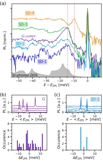
FIG. 2. (a) Comparison of the phonon-sideband for the
defects with a ZPL. Spectra are normalized to the ZPL
max-imum and plotted with respect to their ZPL energy EZP L.
The vertical lines show the position of the first phonon replica at 9.5 meV and 14.5 meV. The gray-shaded area indicates the silicon-phonon density of states. (b-c) (top) Typical PL spec-tra measured on individual defects for families G and SD-2 respectively. Spectra are plotted with respect to the mean
ZPL energy position hEZP Li. (bottom) Distribution of the
ZPL energy shift compare to the middle energy.
tense for families SD-3 and SD-4, until not being de-tectable for families SD-5 and SD-6 (Fig. 1(c)). The Debye-Waller factor (DW) meters the proportion of pho-tons emitted in the ZPL and provides information about the electron-phonon coupling [26]. As indicated in Table I, it reaches values as high as 35% and 25 % for SD-1 and SD-2 defects respectively, whereas it is limited to 2-3 % for families SD-2-3 and SD-4. A closer inspection of the phonon-sideband (PSB) reveals that the first phonon replica appears either at 9.5 meV (SD-4) or at 14.5 meV (SD-1 to SD-3, G-center), as depicted on Figure 2(a) and Table I. We note that the PSB of family SD-6 exhibits a periodicity of 9.5 meV. Since these energies do not
corre-spond to any of the maxima of the silicon-phonon density of states (Fig. 2(a)), the vibronic spectrum likely results from phonons combining localized and Bloch vibrational states [27].
Comparing the ZPL position for the most prevalent families SD-2 and G shows two radically di↵erent dis-tributions. The ZPL position randomly spreads over 20 meV around 977 meV for the G-centers due to local strain variations [28] (Fig. 2 (b)). By contrast, the ZPL of SD-2 defects is always found at three di↵erent energies equally split by 3 meV around 856 meV(Fig. 2(c)). Such a behav-ior suggests three defect configurations for SD-2 defects, which are less sensitive to local strain fluctuations, an appealing property in the prospects of indistinguishable single-photon emission [29]. We note that the average ZPL position for SD-2 centers matches the 856-meV value reported for interstitial carbon defects [25]. Advanced theoretical calculations would be required to explain the observed ZPL distribution.
FIG. 3. (a) Emission polarization diagram measured on single defects from families SD-1 to SD-4. The PL signal is recorded while rotating a polarizer in the detection path and corrected from background counts. The 0 and 90 directions match
the crystal axes [110] and [1¯10]. Solid lines are fits using a
cos2(✓) function. (b) Time-resolved PL decay recorded on
the same defects under 50-ps pulse excitation at 532 nm. The excited-state lifetime is extracted by fitting the data with a single exponential function (solid line). Data related to SD-5 and SD-6 defects can be found in SI.
Besides being near-infrared single-photon emitters, these single defects in silicon share additional interest-ing PL properties. First, these individual emitters are
4 perfectly photostable, with neither blinking nor bleaching
observed while recording their PL signals over time. Fur-thermore, no center fades away after room-temperature warming-up followed by cooling-down to 10K, except the defects of family SD-5 that either disappear or appear in optical scans (see SI). Then, like individual G-centers in silicon [18], these novel single-photon emitters show a bright emission under green optical excitation, with PL intensity at saturation on the order of 10-20 kcounts/s (Table I). These PL count rates are high considering the poor quantum efficiency of our detectors (only 10%) and that we collect at best 2% of the emitted photons due to the high refractive index of silicon (n⇠ 3.5) [18]. At last, all defect families emit linearly-polarized single photons. As shown on Figure 3(a) for families SD-1 to SD-4, each of the PL polarization diagrams measured on individ-ual centers shows the characteristic emission of a single dipole [30] (see SI for families SD-5 and SD-6). Although the interstitial Si atom inside the G-centers as well as in-terstitial carbons are reported to be mobile respectively above 30K [31] and 77K [20], we did not observe any change in the emission polarization diagram of G- and SD-2 defects neither at 130K and 70K respectively nor after successive thermal cycles of the cryostat (see SI).
To characterize the relaxation dynamics of the individ-ual single-photon emitters, we performed time-resolved PL measurements under 532-nm pulse excitation. The photon histograms recorded on single defects belonging to families SD-1 to SD-4 are shown on Figure 3(b). For those four families, we observe a mono-exponential de-cay providing a single excited-state (ES) lifetime rang-ing between 14 ns to 30 ns (Table I). On the contrary, families SD-5 and SD-6 feature a bi-exponential decay, with a short lifetime roughly at 5 ns and a long one around 19 ns and 35 ns respectively (see Table I & SI). All these values are orders of magnitude shorter than the ones measured on emitter ensembles in silicon, such as erbium dopants [9] or T-centers [8]. Consequently, these defects are already advantageous to develop bright Si-based single-photon sources even without requiring PL enhancement by Purcell-e↵ect [32].
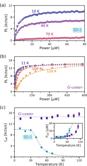
We finally analyze the PL saturation curves as a func-tion of temperature. Here we focus on the most frequent families SD-2 and G (Fig. 1(d)). Figures 4 (a-b) show the PL intensity evolution with optical power P at di↵erent temperatures for two single SD-2 and G-defects. Data follow the behavior from a two-level system modeled by the standard saturation equation:
I(P ) = Isat
P P + Psat
(1) with Isat being the maximum PL intensity at
satura-tion and Psat the saturation power. We observe for
both defects a rise of Psat with increasing temperature
(Fig. 4(c) Inset). This behavior stems from the ther-mal activation of non-radiative decay channels, as
evi-FIG. 4. (a-b) Background-corrected PL saturation curves
measured respectively on a single G-defect and a single SD-2 defect for di↵erent temperatures. Data is fitted with Eq. 1 to
extract the saturation power Psatand intensity at saturation
Isat. (c) Corresponding evolution of Isatand Psat(inset) with
temperature for the SD-2 (blue) and G- (purple) defects. The
dash lines are data fitting (see main text for Psatdata). The
Isat data for the SD-2 defect are fairly reproduced by the
function: a0/(1 + b0exp( Ea2/(kBT )), where a0 and b0 are
free parameters, and Ea2= 24± 3 meV the activation energy.
The dotted line for the G-data is a guide for the eye.
denced by the decrease of ES lifetimes at elevated tem-peratures [21] (see SI). The evolution of Psat with
tem-perature T is fitted with: a + b exp( Ea1/(kBT )), with a
and b as free constants, kB the Boltzmann constant and
Ea1the activation energy that gives the respective values
E(SD 2)a1 = 25± 1 meV and Ea1(G)= 95± 9 meV for SD-2 and G-defects. The most striking feature is related to the PL intensity at saturation: while Isat drops quickly
above 30K for the family SD-2, it stays constant for G-centers well-above the 77K-liquid nitrogen temperature
5 (Fig. 4). Since the PL counts mirror the ES population
of the emitters, this indicates that the G-defects behave as a closed-system when the temperature raises whereas the SD-2 defects are coupled to their environment.
In conclusion, we report the isolation at single scale of new optically-active point defects in silicon. These novel individual emitters provide a wide diversity of bright, linearly-polarized single-photon emission in the near-infrared range, matching the O- and C-telecom bands. We further demonstrate that some single defects exhibit additional appealing properties such as a small spread of the ZPL energies or a strong PL intensity well above the liquid-nitrogen temperature.
This multitude of fluorescent artificial atoms available in silicon could open a new path in exploring Si-based quantum technologies. These single defects could serve as building blocks to develop efficient and determinis-tic sources of photonic qubits in a material widely used for integrated photonics applications [7, 33]. Combin-ing optical and microwave magnetic excitations could en-able to investigate the spin properties attached to these unidentified new single-photon emitters, in view of isolat-ing individual spin-photon interfaces in silicon operatisolat-ing at telecom wavelength [8]. The advance nanotechnology based on this semiconductor, combined with the myr-iad of available defects [20, 34] points the way towards thriving quantum applications based on single defects in silicon [10, 35].
[1] Y. Yoshida and G. Langouche, eds., Defects and Impu-rities in Silicon Materials: An Introduction to Atomic-Level Silicon Engineering, vol. 916 of Lecture Notes in Physics. Tokyo: Springer Japan, 2015.
[2] H. J. Queisser and E. E. Haller, “Defects in Semiconduc-tors: Some Fatal, Some Vital,” Science, vol. 281, pp. 945– 950, Aug. 1998.
[3] A. Morello, J. J. Pla, F. A. Zwanenburg, K. W. Chan,
K. Y. Tan, H. Huebl, M. M¨ott¨onen, C. D. Nugroho,
C. Yang, J. A. van Donkelaar, A. D. C. Alves, D. N. Jamieson, C. C. Escott, L. C. L. Hollenberg, R. G. Clark, and A. S. Dzurak, “Single-shot readout of an electron spin in silicon,” Nature, vol. 467, pp. 687–691, Oct. 2010. [4] Y. He, S. K. Gorman, D. Keith, L. Kranz, J. G. Keizer, and M. Y. Simmons, “A two-qubit gate between phos-phorus donor electrons in silicon,” Nature, vol. 571, p. 371, July 2019.
[5] M. Steger, K. Saeedi, M. L. W. Thewalt, J. J. L. Mor-ton, H. Riemann, N. V. Abrosimov, P. Becker, and H.-J. Pohl, “Quantum Information Storage for over 180 s Us-ing Donor Spins in a 28Si “Semiconductor Vacuum”,” Science, vol. 336, pp. 1280–1283, June 2012.
[6] K. J. Morse, R. J. S. Abraham, A. DeAbreu, C. Bowness, T. S. Richards, H. Riemann, N. V. Abrosimov, P. Becker, H.-J. Pohl, M. L. W. Thewalt, and S. Simmons, “A pho-tonic platform for donor spin qubits in silicon,” Science
Advances, vol. 3, p. e1700930, July 2017.
[7] J. W. Silverstone, D. Bonneau, J. L. O’Brien, and M. G. Thompson, “Silicon Quantum Photonics,” IEEE Jour-nal of Selected Topics in Quantum Electronics, vol. 22, pp. 390–402, Nov. 2016.
[8] L. Bergeron, C. Chartrand, A. T. K. Kurkjian, K. J. Morse, H. Riemann, N. V. Abrosimov, P. Becker, H.-J. Pohl, M. L. W. Thewalt, and S. Simmons, “A silicon-integrated telecom photon-spin interface,”
arXiv:2006.08793 [cond-mat, physics:physics], June
2020. arXiv: 2006.08793.
[9] L. Weiss, A. Gritsch, B. Merkel, and A. Reiserer, “Erbium dopants in silicon nanophotonic waveguides,” arXiv:2005.01775 [physics, physics:quant-ph], May 2020. arXiv: 2005.01775.
[10] J. R. Weber, W. F. Koehl, J. B. Varley, A. Janotti, B. B. Buckley, C. G. Van de Walle, and D. D. Awschalom, “Quantum computing with defects,” Proceedings of the National Academy of Sciences, vol. 107, pp. 8513–8518, May 2010.
[11] I. Aharonovich, D. Englund, and M. Toth, “Solid-state single-photon emitters,” Nature Photonics, vol. 10, pp. 631–641, Oct. 2016.
[12] G. Zhang, Y. Cheng, J.-P. Chou, and A. Gali, “Material platforms for defect qubits and single-photon emitters,” Applied Physics Reviews, vol. 7, p. 031308, Sept. 2020.
[13] A. Gruber, A. Dr¨abenstedt, C. Tietz, L. Fleury,
J. Wrachtrup, and C. v. Borczyskowski, “Scanning Con-focal Optical Microscopy and Magnetic Resonance on Single Defect Centers,” Science, vol. 276, pp. 2012–2014, June 1997.
[14] C. Bradac, W. Gao, J. Forneris, M. E. Trusheim, and I. Aharonovich, “Quantum nanophotonics with group IV defects in diamond,” Nature Communications, vol. 10, p. 5625, Dec. 2019. Number: 1 Publisher: Nature Pub-lishing Group.
[15] D. J. Christle, A. L. Falk, P. Andrich, P. V. Klimov, J. U. Hassan, N. T. Son, E. Janz´en, T. Ohshima, and D. D. Awschalom, “Isolated electron spins in silicon car-bide with millisecond coherence times,” Nature Materi-als, vol. 14, pp. 160–163, Feb. 2015.
[16] M. Widmann, S.-Y. Lee, T. Rendler, N. T. Son, H. Fedder, S. Paik, L.-P. Yang, N. Zhao, S. Yang, I. Booker, A. Denisenko, M. Jamali, S. A. Momen-zadeh, I. Gerhardt, T. Ohshima, A. Gali, E. Janz´en, and J. Wrachtrup, “Coherent control of single spins in silicon carbide at room temperature,” Nature Materials, vol. 14, pp. 164–168, Feb. 2015.
[17] T. T. Tran, K. Bray, M. J. Ford, M. Toth, and I. Aharonovich, “Quantum emission from hexagonal
boron nitride monolayers,” Nature Nanotechnology,
vol. 11, pp. 37–41, Jan. 2016.
[18] W. Redjem, A. Durand, T. Herzig, A. Benali, S. Pezza-gna, J. Meijer, A. Y. Kuznetsov, H. S. Nguyen, S. Cu-e↵, J.-M. G´erard, I. Robert-Philip, B. Gil, D. Caliste, P. Pochet, M. Abbarchi, V. Jacques, A. Dr´eau, and G. Cassabois, “Single artificial atoms in silicon emitting at telecom wavelengths,” arXiv:2001.02136 [cond-mat,
physics:physics, physics:quant-ph], Jan. 2020. arXiv:
2001.02136.
[19] M. Hollenbach, Y. Berenc´en, U. Kentsch, M. Helm, and G. V. Astakhov, “Engineering telecom single-photon emitters in silicon for scalable quantum photonics,” Op-tics Express, vol. 28, pp. 26111–26121, Aug. 2020.
Pub-6
lisher: Optical Society of America.
[20] G. Davies, “The optical properties of luminescence cen-tres in silicon,” Physics Reports, vol. 176, pp. 83–188, May 1989.
[21] C. Beaufils, W. Redjem, E. Rousseau, V. Jacques, A. Y. Kuznetsov, C. Raynaud, C. Voisin, A. Benali, T. Herzig, S. Pezzagna, J. Meijer, M. Abbarchi, and G. Cassabois, “Optical properties of an ensemble of G-centers in sili-con,” Physical Review B, vol. 97, p. 035303, Jan. 2018. [22] C. Chartrand, L. Bergeron, K. J. Morse, H.
Rie-mann, N. V. Abrosimov, P. Becker, H.-J. Pohl,
S. Simmons, and M. L. W. Thewalt, “Highly
en-riched $ˆ{28}\mathrm{Si}$ reveals remarkable optical
linewidths and fine structure for well-known damage cen-ters,” Physical Review B, vol. 98, p. 195201, Nov. 2018. [23] A. Beveratos, R. Brouri, J.-P. Poizat, and P. Grangier,
“Bunching and Antibunching from Single NV Color Cen-ters in Diamond,” in Quantum Communication, Com-puting, and Measurement 3 (P. Tombesi and O. Hirota, eds.), pp. 261–267, Boston, MA: Springer US, 2002. [24] M. D. Eisaman, J. Fan, A. Migdall, and S. V. Polyakov,
“Invited Review Article: Single-photon sources and
detectors,” Review of Scientific Instruments, vol. 82, p. 071101, July 2011. Publisher: American Institute of Physics.
[25] K. Thonke, A. Teschner, and R. Sauer, “New photolu-minescence defect spectra in silicon irradiated at 100 K: Observation of interstitial carbon?,” Solid State Commu-nications, vol. 61, pp. 241–244, Jan. 1987.
[26] C. E. Dreyer, A. Alkauskas, J. L. Lyons, A. Janotti, and C. G. Van de Walle, “First-Principles Calculations of Point Defects for Quantum Technologies,” Annual Re-view of Materials Research, vol. 48, no. 1, pp. 1–26, 2018. [27] S. K. Estreicher, D. West, J. Goss, S. Knack, and J.
We-ber, “First-Principles Calculations of Pseudolocal Vibra-tional Modes: The Case of Cu and Cu Pairs in Si,” Phys-ical Review Letters, vol. 90, p. 035504, Jan. 2003. Pub-lisher: American Physical Society.
[28] V. D. Tkachev and A. V. Mudryi, “Piezospectroscopic ef-fect on zero-phonon luminescence lines of silicon,” Jour-nal of Applied Spectroscopy, vol. 29, pp. 1485–1491, Dec. 1978.
[29] A. Sipahigil, K. Jahnke, L. Rogers, T. Teraji, J. Isoya, A. Zibrov, F. Jelezko, and M. Lukin, “Indistinguishable Photons from Separated Silicon-Vacancy Centers in Di-amond,” Physical Review Letters, vol. 113, p. 113602, Sept. 2014.
[30] R. J. Elliott, I. G. Matthew, and E. W. J. Mitchell, “The polarization of luminescence in diamond,” Philosophical Magazine, vol. 3, pp. 360–369, Apr. 1958.
[31] K. P. O’Donnell, K. M. Lee, and G. D. Watkins, “Origin of the 0.97 eV luminescence in irradiated silicon,” Physica B+C, vol. 116, no. 1, pp. 258–263, 1983.
[32] E. M. Purcell, H. C. Torrey, and R. V. Pound, “Res-onance Absorption by Nuclear Magnetic Moments in a Solid,” Physical Review, vol. 69, pp. 37–38, Jan. 1946. [33] X. Qiang, X. Zhou, J. Wang, C. M. Wilkes, T. Loke,
S. O’Gara, L. Kling, G. D. Marshall, R. Santagati, T. C. Ralph, J. B. Wang, J. L. O’Brien, M. G. Thompson, and J. C. F. Matthews, “Large-scale silicon quantum photon-ics implementing arbitrary two-qubit processing,” Nature Photonics, vol. 12, p. 534, Sept. 2018.
[34] P. Pichler, Intrinsic Point Defects, Impurities, and Their
Di↵usion in Silicon. Computational Microelectronics,
Wien: Springer-Verlag, 2004.
[35] P. M. Koenraad and M. E. Flatt´e, “Single dopants in semiconductors,” Nature Materials, vol. 10, pp. 91–100, Feb. 2011.