Automated Design Synthesis of CMOS
Operational Amplifiers
by
Ognen J. Nastov
S.B. Elect. Eng., Massachusetts Institute of Technology (1991)
Submitted to the Department of Electrical Engineering and
Computer Science
in Partial Fulfillment of the Requirements for the Degree of
Master of Science
at the Massachusetts Institute of Technology
February 1994
®
Ognen J. Nastov, 1994
The author hereby grants to MIT permission to reproduce and
to distribute copies of this thesis document in whole or in part.
Signature of Author ...
O ...
Department of Electrical Engineering and Computer Science
January 19, 1994
Certified
by... . ... ...
.)
Gerald J. Sussman
Matsushita Professor of Electrical Engineering
n
C71
god
.
Thesis Supervisor
Automated Design Synthesis of CMOS Operational
Amplifiers
by
Ognen J. Nastov
Submitted to the Department of Electrical Engineering and Computer Science January 19, 1994
In Partial Fulfillment of the Requirements for the Degree of Master of Science
Abstract
In this thesis, I designed and implemented a system which autonomously designs optimal CMOS operational amplifiers. Throughout the design search, my system assembles the op amps by composing subcircuits. I evaluate op amps' performances by applying symbolic transformations and numerical techniques to the set of asserted approximate design equations. I also implemented a simulator-based performance evaluator that verifies the optimal designs.
My system controls the optimal design quest with a robust genetic algorithm. I integrate the searches through the topological and design parameter spaces in a novel, unique way. As a result, my system's design search is efficient, exhaustive, global, unbiased, and autonomous.
My system also designs op amps following an alternative strategy inspired by observation of human designers. In addition, my system autonomously generates such strategies.
Finally, I demonstrate my system's ability to autonomously design optimal CMOS op amps through a number of successful design experiments: a minimal area, high speed, micropower, high bandwidth, and high gain optimal designs.
This report describes research done at the Artificial Intelligence Laboratory of the Massachusetts Institute of Technology. Support for this research is provided in part by the Advanced Research Projects Agency of the Department of Defense under Office of Naval Research contract N00014-92-J-4097 and by the National Science Foundation under grant number MIP-9001651.
Thesis Supervisor: Gerald J. Sussman
Acknowledgements
I would like to express my thanks to all the people who have contributed in one way
or another to the realization of this thesis:
My thesis advisor Gerry Sussman for his continued support, skillful guidance, and valuable advice on all aspects of this thesis.
Hal Abelson, for his constant understanding and support, and for overseeing my early circuit optimization work.
Dr. Amar Bose, for his friendship, and for sharing his unique vision of the worlds of teaching, acoustics, and linear circuits with me.
Mark Jakiela, for introducing me to the world of genetic algorithms. Greg Allen, for his friendship and review of an early draft of this thesis.
Phillip Alvelda, Bill Rozas, Chris Hanson, and other AI lab members for answering questions on MOS technology, scheme, and other topics.
The Neilys, the Browns, the Sarginsons, and others, for their friendship. M.I.T. Varsity Swimming, for helping me stay in excellent physical shape. The U.S. Army, for stationing 300 peacekeeping troops in Macedonia.
Finally, my mother Svetlana and sister Vesna, for their endless love, encouragement, and unwavering support in every part of my life.
Contents
1 Introduction 13
1.1 Operational Amplifier Design Overview . . . ... 14
1.2 Previous VLSI Design Automation Efforts ... 15
1.3 Organization of Thesis ... 18
2 Design Example: An Optimal High Speed Op Amp 21 3 Modular Composition Scheme 43 3.1 Overview . . . ... 43
3.2 Op Amp Topological Template . . . 45
3.2.1 Topology Selection Strategy . . . ... 47
3.3 Object-Oriented Implementation Approach . ... 49
3.3.1 Object Structure ... 49
4 Op Amp Performance Evaluation 55 4.1 Approximate Design Equation Performance Evaluator ... 55
4.1.1 Design Equations . . . ... 57
4.1.2 Equation Solving Language ... 59
4.2 Simulator Based Performance Evaluator ... 62
5.1 5.2 5.3 5.4 5.5
Why a Genetic Algorithm? ... A Simple Genetic Algorithm ... Coding of Design Parameters ...
GA Design Strategy Setup and Runtime Parameters Choice
Fitness Function Structure ...
71
74
75
77 80
6 Alternative Design Strategies
6.1 Design Strategy Inspired by Observation of Human Designers (First-Cut) 6.1.1 First-Cut Design Example.
6.2 Automated Generation of First-Cut Design Procedures ...
7 Design Experiments
7.1 Minimal Area Op Amp Design ... 7.2 An Optimal Micropower Op Amp ... 7.3 An Optimal High Bandwidth Op Amp ....
7.4 In Search of A High Gain Op Amp ...
8 Conclusion 8.1 Contributions of Thesis . 8.2 Future Work . 83 83 86 92 97 97 105 105 113 115 115 116
A Subcircuit Modules and Circuit Components
A.1 Circuit Diagrams of Subcircuit Modules . . . A.2 Design Equations for the Op Amp Object . . A.3 Subcircuit Objects.
A.3.1 Current Mirrors (CM) ... A.3.2 Differential Stages (DS) ... A.3.3 Current Sources (CS) ... A.3.4 Output Stages (OS) ...
119 ... . . . 119 ... . . . 124 ... . . . 124 ... . . . 124 ... . . . 127 ... . . . 128 ... . . . 128
A.4 Circuit Component Objects ... 133
A.4.1 MOS Transistors ... . 133
A.4.2 Other Components ... . 135
13 MOS Device Models 137 _B.1 Device Model Constants ... 137
B.2 MOS Large-Signal Device Model ... .. 139
B.3 Small-Signal MOS Model ... 141
_B.4 Design Defaults ... 143
C Op Amp Analysis Summary 145 C.1 Performance Functions ... 145
List of Tables
2.1 High speed op amp design parameter specifications ... 21 2.2 High speed op amp performance specifications ... 22 2.3 Design parameters for the best op amp in the initial generation of the
high speed design run. ... 26 2.4 Performance summary of the best op amp in the initial generation of
the high speed design run ... 27 2.5 Design parameters of the best op amp in generation 10 of the high
speed design run . ... 28 2.6 Performance summary of the best op amp in generation 10 of the high
speed design run . ... 29 2.7 Design parameters for the best op amp in generation 30 of the high
speed design run . ... 30 2.8 Performance summary of the best op amp in generation 30 of the high
speed design run ... 31 2.9 Design parameters for the best op amp in generation 40 of the high
speed design run . ... 32 2.10 Performance summary of the best op amp in generation 40 of the high
speed design run . ... 33 2.11 Design parameters for the best op amp in generation 50 of the high
2.12 Performance summary of the best op amp in generation 50 of the high speed design run ...
2.13 Design parameters for the best op amp in generation 120 of the high speed design run ...
2.14 Performance summary of the best op amp in generation 120 of the high speed design run ...
2.15 Optimal design parameters for a high speed op amp ... 2.16 Optimal high speed op amp performance summary ... 5.1
5.2 5.3
Coding of op amp design parameters ... Precision of the design parameter coding ...
GA default design strategy setup and run-time parameters 6.1 Simple two stage op amp design parameter specifications ... 6.2 Simple two stage op amp performance specifications ...
6.3 First-cut and GA computed design parameters for a simple two stage
op amp . ...
6.4 First-cut designed simple two stage op amp performance summary . . 6.5 GA designed simple two stage op amp performance summary ...
Minimal area op amp design parameter specifications . . Minimal area op amp performance specifications ... Optimal design parameters for a minimal area op amp Minimal area op amp performance summary ... Maximal UGB op amp performance specifications .... Optimal design parameters for a maximal UGB op amp . Maximal UGB op amp performance summary ...
. . . ... . . 98
... . .99
... . . . 100 ... . . . 101 ... ... . 106 ... . . . 109 ... . . . 110B.1 Physical and Silicon Constants ...
35 36 37 38 39 77 78 79 87 88 89 90 91 7.1 7.2 7.3 7.4 7.5 7.6 7.7 137
List of Figures
1-1 An operational amplifier. . ... ... 15 2-1 Topology of the best op amp in the initial generation of the high speed
design
run
...
.
...
...
26
2-2 Topology of the best op amp in generation 10 of the high speed design
run ... 28
2-3 Topology of the best op amp in generation 30 of the high speed design
run ... . 30
2-4 Topology of the best op amp in generation 40 of the high speed design run ... 32 2-5 Topology of the best op amp in generation 50 of the high speed design
run ... 34
2-6 Topology of the best op amp in generation 120 of the high speed design run ... 36 2-7 Optimal high-speed op amp topology ... 38 2-8 Genetic algorithm convergence profile for the high speed op amp design
run ... 40
2-9 DC characteristics of the optimal high speed op amp ... 40 2-10 Frequency domain behavior of the optimal high speed op amp ... . 41 2-11 Switching characteristics of the optimal high speed op amp ... 41
Topological template for op amps ... Subcircuit styles summary ...
Code listing for the simple differential stage object ...
Large signal (top) and small signal (bottom) circuit diagrams of the simple differential stage module ...
Op amp performance evaluation ... Measurement of the input CMR ... Measurement of the output swing ...
Measurement of the input offset and power dissipation . . Measurement of the differential gain, UGB frequency, and Measurement of the common-mode gain and CMRR .... Measurement of the PSRR+ (left) and PSRR- (right) . . . Measurement of the slew rate and settling time ...
Crossover and mutation ...
Op amp chromosome structure ... Topology phene structure ...
A simple two-stage op amp first-cut design procedure . . . Two stage Miller compensated op amp ...
Main loop of a prototype program for automated first-cut
... .. 56
... . .66
... . .66
... . .66
)hase margin 67 . . . ... . . 68. . . ...
... 68
. . . ... ... 69
...
.75
... . .76
... . .78
85 86 procedure . procedure generation . . . 936-4 Partial design node network for a simple two-stage Miller compensated op amp ... Minimal area op amp topology ... DC characteristics of the minimal area op amp ... Frequency domain behavior of the minimal area op amp ... . . . 100 ... ... . 102
... 103
3-2 3-3 3-4 3-5 46 47 50 51 4-1 4-2 4-3 4-4 4-5 4-6 4-7 4-8 5-1 5-2 5-3 6-1 6-2 6-3 7-1 7-2 7-3 947-5 Maximal UGB op amp topology ...
7-6 DC characteristics of the maximal UGB op amp ... 7-7 Frequency domain behavior of the maximal UGB op amp 7-8 Switching characteristics of the maximal UGB op amp A-1 Current source module design styles
A-2 Current mirror module design styles . A-3 Differential stage module design styles A-4 Output; stage module design styles . . . A-5 Compensation module design styles B-1 Large-signal MOS transistor model B-2 Top view of a MOS transistor ... B-3 Small-signal MOS transistor model . . C-1 Top view of CMOS resistor ...
C-2 Op amp small-signal equivalent circuit
... . . . 119 ... . . . 120 ... . . . 121 ... . . . 122 ... . . . 123 ... . . . 139 ... . . . 141 ... . . . 142 ... . . . 146 ... . . . 148 108 111 112 112
Chapter 1
Introduction
In this thesis, I designed and implemented a system which autonomously designs optimal CMOS operational amplifiers. Throughout the design search, my system assembles the op amps by composing subcircuits. I evaluate op amps' performances by applying symbolic transformations and numerical techniques to the set of asserted approximate design equations. I also implemented a simulator-based performance evaluator that verifies the optimal designs.
My system controls the optimal design quest with a robust genetic algorithm. I integrate the searches through the topological and design parameter spaces in a novel, unique way. As a result, my system's design search is efficient, exhaustive, global, unbiased, and autonomous.
My system also designs op amps following an alternative strategy inspired by observation of human designers. In addition, my system autonomously generates such strategies.
Finally, I demonstrate my system's ability to autonomously design optimal CMOS op amps through a number of successful design experiments: a minimal area, high
1.1 Operational Amplifier Design Overview
The integration of analog and digital systems in the same package has become a widespread accepted engineering practice due to the continual increase in chip com-plexity. A number of feature-packed, sophisticated, and robust CAD tools can today be used to design the digital gate arrays, cells, and macro cells on such chips. In con-trast, most analog circuit blocks still have to be designed by hand because: (1) analog circuits are not as easily decoupled into a set of simple interconnected basic blocks as digital circuits are; (2) device non-linearities are more important in analog circuit design, making the design process a knowledge-intensive task, and requiring experts with an accumulated set of techniques, approximation tricks, and circuit intuition; and (3) the performance specifications for analog circuits are more numerous, varied, and complicated than those for digital circuits.
The analog and digital system integration constrains the designers to using the same VLSI processing technology for both the analog and digital parts. The domina-tion of the CMOS technology in today's monolithic digital systems has thus singled out CMOS as a dominant technology for integrated analog circuit systems.
One of the most important and widely used analog blocks is the operational am-plifier (op amp), shown in Figure 1-1. The objective of the op amp is to amplify the difference between its two input signals v+ and v_. The op amp has to exhibit large amplification (gain) since its primary use is in implementing signal processing functions through the use of negative feedback.
Op amps are the functional core of many mixed analog/digital VLSI systems, par-ticularly interface circuits, such as A/D and D/A converters, and switched capacitor filters.
Op amps are characterized by a large number of mutually conflicting performance specifications with variable priorities which depend on the op amp functionality within the analog system. For example, op amps used as comparators in A/D converters
v out
Figure 1-1: An operational amplifier
and power dissipation (an N-bit flash A/D converter employs 2N op amps on a single
chip). In contrast, op amps used in filtering applications or other negative-feedback configurations have to be compensated, i.e., are required to have high gain, and solid phase margins.
The human analog circuit designer goes through several phases when designing an op amp. In the first phase, the designer considers the intended application of the op amp, sets the performance specifications, and decides upon an appropriate circuit topology. In the second phase, the topology is sized and biased using analytical first-order design equations. In the third phase, the design is evaluated and optimized by adjustments of the design parameters and repeated circuit simulation. At the completion of the third phase, the op amp design is ready to be laid out and fabricated for testing. A survey of analog VLSI circuit designers [14] has indicated that the third design phase is the primary bottleneck of the analog circuit design process.
1.2 Previous VLSI Design Automation Efforts
During the past 10-15 years, varied methodologies have been employed in systems that automate the analog VLSI design process. These systems differ in three main areas: the circuit topology selection scheme (if any), the choice of a circuit perfor-mance evaluator, and the featured optimization method (if any). The optimization is typically carried out by having one performance function (such as the circuit chip
function, while the rest of the circuit performances are set up as constraints.
In 1983, Nye et al [20] developed Delight.Spice, a system which uses the data output from a general-purpose circuit simulator to evaluate each design point (iter-ation) of a fixed-topology analog circuit. This system employs a feasible directions optimization scheme to guide the iterations.
The advantage of using a circuit simulator as a performance evaluator lies in its accuracy, generality, and applicability to a broad range of circuits. Circuit simulators accurately predict circuit behavior because they employ complex and extensive de-vice models, and use a variety of numerical techniques to solve the large systems of non-linear differential equations that describe the circuit. On the other hand, using circuit simulators as performance evaluators results in high computational intensity, especially for large circuits. In addition, circuit simulators can easily fail to converge for unorthodox sets of design parameters produced by the design search of the outer optimization driver loop.
Another approach in evaluating the circuit performance is to use approximate analytic 1-st order design equations. This approach is less intensive regarding com-puter resources, but requires development of such equations for each particular circuit topology or circuit building block. In addition, this scheme is less accurate than the method of using a circuit simulator. This in turn means that the solutions achieved in this scheme may in fact be only near-optimal.
Sometimes the accuracy of the equations used in this approach are enhanced by introducing fitting parameters. The results of a particular equation are fitted with the results obtained from repeated circuit simulations. Nevertheless, this fitting scheme
has met limited success [15].
A number of authors developed systems built around a performance evaluator based on a set of approximate equations. In some cases, for example in the CIROP system (1984) by Ressler [23], the IDAC system (1987) by DeGrauwe et al [7], and
composing subcircuit modules and solving the appropriate design equations until the designed circuit satisfies the design specifications, thus closely mimicking the human design approach. These systems do not feature any optimization schemes. The problem with this approach is that it does not yield optimal designs, although it does provide a good starting point for a circuit optimizer.
The approaches that employ an optimization algorithm include OPASYN by Koh (1989) [15], and the work done by Maulik and Carley (1991) [17]. Koh first heuris-tically selects an op amp topology from a library of four topologies, and then uses a steepest descent unconstrained method to optimize the design. Maulik and Car-ley also start from a fixed circuit topology and feature a constrained optimization
method.
A common problem that arises from applying a general-purpose optimizer is the need for a good initial guess. When a circuit simulator is used as a performance eval-uator, the computed performance functions tend to be noisy and non-differentiable. This constrains the optimization methods to be of zero-order only, which somewhat alleviates the problems of converging to a local minimum (or even to a local noise
spike) when the optimization is started from a random initial point.
When a carefully crafted set of 1-st order design equations is used in circuit perfor-mance evaluation, the restriction on the order of the optimization methods can usually be lifted, and standard constrained NLP methods can then be used [17]. Nevertheless, the requirement for a good initial guess, and the problem of converging to a true local minimum remain. In addition, as mentioned above, at best constrained NLP methods arrive only in the vicinity of the actual optimal solution due to the inaccuracies in the approximate circuit performances from the analytic design equations.
In the cases when the performance functions are approximately computed, and are continuous and differentiable, in addition to the problem of converging to local minima, constrained optimization methods may also fail because they may be unable
To the best of my knowledge, my application of genetic algorithms (GAs) to the problem of finding an optimal analog circuit design in this thesis and in my pre-vious fixed topology optimal study [19] is original. Genetic algorithms are robust iterative general purpose zero-order unconstrained search strategies based on ideas from population genetics and natural selection [10]. They maintain a population that evolves and improves with each generation (iteration). These algorithms are intrin-sically global in nature and thus somewhat alleviate the local minimum convergence problem. GAs do not require a good initial point to start the search. Genetic algo-rithms also exhibit potential for a full parallelization, which would make them even more attractive as the current trend of proliferation of parallel computer hardware continues.
In this thesis, I present a system for automated synthesis of CMOS op amps, whose main features are a modular subcircuit composition technology, an approxi-mate design equations performance evaluator, and a genetic algorithm optimization scheme. The equation-based performance evaluator is built around a mixed sym-bolic and numerical algebraic equation solving scheme. My system also includes a circuit simulator-based performance evaluator, which verifies the designed op amps. This evaluator is based on a two-way interface to a circuit simulator which performs various op amp experiments, and a package that processes raw simulator data. A featured genetic algorithm evolves a population of topologically and parametrically varied op ams, and allows the survival and reproduction of the fittest among the op amps through a structured and partially randomized genetic information exchange. My system also features a design strategy inspired by observation of human designers
1.3 Organization of Thesis
Chapter 2 demonstrates an op amp design example. Chapter 3 presents the modular composition technology, a core idea in my system's design methodology. Chapter 4 describes the schemes used to evaluate the performance of the op amps. Chapter 5 details on the main genetic algorithm based design strategy. Chapter 6 discusses some additional design strategies featured in my system. Chapter 7 features additional op amp design experiments. In Chapter 8 I summarize my work and detail on possible fiuture research directions.
The Appendix contains the circuit diagrams and the LISP code for all subcircuit modules (objects) and circuit components, a summary of the MOS device models, tabulation of process and design constants and parameters, and a summary overview of the op amp performance functions.
Chapter 2
Design Example: An Optimal
High Speed Op Amp
Op amps used in interface circuits, such as A/D and D/A converters, are primarily required to be of high speed, i.e. to switch as fast as possible. This design goal can be achieved by maximizing the slew rate of the op amp. Thus I gave my system the set of design specifications shown in Table 2.1 and Table 2.2. The penalty forms and coefficients are further discussed in Chapter 5. The technology constants for the simple 5m CMOS process used are given in Table B.2 in the Appendix.
Design Parameters
Design Parameter(s) Allowable Range Transistor sizes M 0.5 100 Compensation capacitor Cc (pF) 0.1 20 Nulling resistor Rz (kQ) 0 100
Bias voltages VBIAS (V) VsS VDD
Design Performance Specifications
Performance Specification Penalty form Penalty coefficient CMOS Technology SIMPLE 5m
-Ambient temperature (C) 25 -Positive power supply VDD (V) 5
Negative power supply Vss (V) -5 -MOS channel lengths L (pm) 10 -Loading capacitance CL (pF) 20
-Active area (m 2) < 50000 linear .01 DC power (mW) < 20 linear 10
Input offset (mV) = 0 linear 10
Input CMR (V) -3 - 3 linear 10 & 30
Output swing (V) -3 -. 3 linear 10 & 30 Differential gain @ DC (dB) > 80 linear 10 CMRR @ DC (dB) > 80 linear 1 Unity gain bandwidth (MHz) > 5 linear 60 Phase margin (degrees) > 60 linear 10 PSRR+ @ DC (dB) > 80 linear 1 PSRR- @ DC (dB) > 80 linear 1
Slew rate (V/ps) MAXIMIZE goal: 100 5
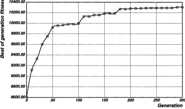
After randomly generating an initial population of thirty op amps with varied modularly composed topologies and parameter values, my system evolved three hun-dred generations of this population. The topologies, design parameters, and perfor-mances of the currently best op amps from a few selected generations in the design run are given in Figures 2-1 - 2-6, and Tables 2.3 - 2.14. (Note that the SPICE veri-fication data is missing from most of these tables. The SPICE circuit simulator based performance evaluator could not verify the performances computed by the approxi-mate equations based performance evaluator due to convergence failures for most of these op amps. The simulator's convergence failures are due to the unorthodoxy of the design parameters for these intermediate circuits, and are further discussed in Chapter 4.)
The genetic algorithm convergence profile is shown in Figure 2-8. The plot shows the continual converging improvement in the fitness function values of the best op amp in each generation. The fitness function summarizes the quality of the op amp's performance in a single number, and is further discussed in Chapter 5.
The fittest individual in the initial generation was a two-stage op amp with cas-coded current mirror loads, cascas-coded differential input stage, and cascas-coded output stage, and no compensation scheme. During the initial fifty generations this topology turned out to be inadequate in satisfying the active area, phase margin, and voltage swing requirements. The evolution mechanisms thus engineered a sequence of bet-ter topological albet-ternatives by virtue of introducing a nulling resistor compensation during the first 10 generations as well as removing the cascode devices from (1) the current mirror loads after thirty generations; (2) from the differential input stage (between generations 30 and 40); and (3) from the output stage (between generations 40 and 50).
The next sixty generations indicated the inability of the currently best op amp topology to achieve the required DC differential gain levels previously obtained by its
nisms induced the expected change in the output stage genes in order to switch back to op amps with a cascoded output stage.
In the remaining 190 generations, this op amp topology, shown in Figure 2-7 en-joyed a stable adjustment in its design parameters inducing a continual improvement of its overall performance, and converged to its optimal parametric configuration summarized in Table 2.15. The achieved performance of this optimal high speed op amp is given in Table 2.16, and its simulation plots in Figure 2-9, Figure 2-10, and Figure 2-11. The fast switching capability of the designed op amp is readily visible from Figure 2-11.
As it can be seen from Table 2.16, the achieved design violates the design require-ments for the input and output voltage swings, and the PSRRs. It is possible to instruct my design system to emphasize these requirements. I have chosen not to do so because in my experience (1) the voltage swing requirements are frequently un-derestimated by the approximate equations used in my system, and (2) the PSRRs, as well as other frequency domain performances are only crudely approximated with the 1-st order equations. I will discuss these and other related issues in the following chapters.
Table 2.16 indicates a large discrepancy between SPICE and design equations computed values for the output resistance. At the same time, the SPICE and design equations computed values of the small signal channel conductances for the devices in the cascoded output stage did match each other very well. I have observed this paradox in other circuits simulated with the particular version of the SPICE program I used (HPSPICE 3.4c). I thus concluded that the SPICE calculation of the output resistance is unreliable due to a bug in the program.
Table 2.16 also shows a discrepancy in the slew rate values. While the design equations determine the slew rate by considering the maximum rate of charging of the compensation capacitor by the first stage current, in this particular circuit it is the
slew rate limit. The ratio of the second stage bias current to the loading capacitance gives a 51 V/s slew rate figure, which is much closer to the SPICE computed value of 41 V/us.
v dd
vout
Figure 2-1: Topology of the best op amp in the initial generation of the high speed design run
Design Parameters
Design Parameter I Allowable Range I Value
M1, M2 0.5 -, 100 36.4 M3, M4 0.5 -'- 100 94.6 M5, M6 0.5 -, 100 83.0 M7, M8 0.5 - 100 54.5 M9 0.5 - 100 22.1 M1 0, M1 1 0.5 ~ 100 76.7 M12, M13 0.5 -* 100 56.3 VBIAS (V) -5 -- 5 -2.20 VBC (V) -5 - 5 2.04 VBP (V) -5 -* 5 1.82 VBN (V) -5 5 .43
Table 2.3: Design parameters for speed design run
Design Performance Summary
Performance Specification Design SPICE Active area (m 2 ) < 50000 55364 -DC power (mW) < 20 21.62 -Input offset (mV) = 0 4.51 -Input CMR (V) -3 3 1.4 , 1.7 -Output swing (V) -3 -, 3 -1.4 0.5 -Differential gain @ DC (dB) > 80 109 -CMRR D)C (dB) > 80 71 -Unity gain bandwidth (MHz) > 5 6.0 -Phase margin (degrees) > 60 3
PSRR+ @ DC (dB) > 80 87 -PSRR- @ DC (dB) > 80 87 -Slew rate (V/ls) MAXIMIZE 78
-Area of Cc (%) - 0
-Area of Rz (%) 0
First stage bias current I(cs) (A) - 611 -Second stage bias current I(os) (A) - 1551 -Output resistance ROUT (KQ) - 796 -Dominant pole pole, (Hz) - 275990
-Output pole poleli (MHz)
-
9.9e-3
-Compensation pole poleli (MHz) -
-Zero
(MHz)
-Table 2.4: Performance summary of the high speed design run
v_dd
vout
Figure 2-2: Topology of the best op amp in generation 10 of the high speed design run
Design Parameters
Design Parameter Allowable Range I Value
M1, M2 0.5 100 24.7 M3, M4 0.5 ' 100 56.9 M5, M6 0.5 '- 100 4.89 M7, M8 0.5 -' 100 27.6 M9 0.5 - 100 30.0 M1o, M1 0.5 100 55.0 M12, M1 3 0.5 ", 100 56.1 Cc (pF) 0.1 _ 20 12.9 Rz (kQ) 0 , 100 4.22 VBIAS (V) -5 ' 5 -3.19 VBC (V) -5 5 1.40 VBP (V) -5- 5 -2.42 VBN (V) -5 -' 5 -4.57
Table 2.5: Design parameters of design run
Design Performance Summary
Performance Specification Design SPICE Active area (m 2) < 50000 78739 -DC power (mW) < 20 4.74 -Input offset (mV) = 0 .06 -Input CMR (V) -3 3 -2.6 - 1.1 -Output swing (V) -3 , 3 -3.4 2.6 -Differential gain @ DC (dB) > 80 159 -CMRR @ DC (dB) > 80 118
Unity gain bandwidth (MHz) > 5 3.4 -Phase margin (degrees) > 60 76 -PSRR+ @ DC (dB) > 80 131 -PSRR- @ DC (dB) > 80 131 -Slew rate (V/ps) MAXIMIZE 12.7
-Area of Cc (%) 38
Area of Rz (%) 11
-First stage bias current I(cs) (A) - 165
Second stage bias current I(os) (A) - 309
-Output resistance ROUT (KQ) - 8136
-Dominant pole polei (Hz) .04 -Output pole pole,, (MHz) 4.1
-Compensation
pole
poleIl (MHz) -29.5
-Zero (MHz:) 5.3
Table 2.6: Performance summary of the best op amp in generation 10 of the high speed design run
v_dd
vout
Figure 2-3: Topology of the best op amp in generation 30 of the high speed design
run
Design Parameters
Design Parameter Allowable Range Value
M1, M2 0.5 - 100 24.7 M3, M4 0.5 '100 4.48 M5, M6 0.5 ,, 100 27.6 M7 0.5 100 78.1 M8, M9 0.5 -, 100 55.2 Mo, 0 M 11 0.5 -100 56.1 Cc (pF) 0.1 -20 10.5 Rz (kQ) 0 - 100 4.27 VBIAS (V) -5 '- 5 -3.19 VBC (V) -5 - 5 1.39 VBP (V) -5 ' 5 -2.41 VBN (V) -5 5 -2.17
Table 2.7: Design parameters for design run
Design Performance Summary
Performance Specification Design SPICE Active area (m 2) < 50000 67635 -DC power (mW) < 20 7.39 -Input offset (mV) = 0 2.83 -Input CMR (V) -3 , 3 -2.2 -, 1.1 -Output swing (V) -3 3 3.4 ' 2.6 -Differential gain @ DC (dB) > 80 113 -CMRR @ DC (dB) > 80 119 -Unity gain bandwidth (MHz) > 5 6.8
-Phase margin (degrees) > 60 65
-PSRR+ @ DC (dB) > 80 85 -PSRR- @ DC (dB) > 80 85 -Slew rate (V/ps) MAXIMIZE 41 -Area of Cc (%) - 36
-Area of Rz (%) 13
-First stage bias current I(cs) (A) - 430 -Second stage bias current I(os) (A) - 309
-Output resistance ROUT (KQ) - 8145
-Dominant pole pole, (Hz) 15.4
-Output pole polei (MHz) 4.15
-Compensation pole polei, (MHz) - 29.0
-Zero (MHz) -
6.43-Table 2.8: Performance summary of the speed design run
v_dd
v out
Figure 2-4: Topology of the best op amp in generation 40 of the high speed design run
Table 2.9: Design parameters for the design run
best op amp in generation 40 of the high speed Design Parameters
Design Parameter Allowable Range
I
ValueM1, M2 0.5 -~, 100 24.7 M3, M4 0.5 -100 27.1 M5 0.5 -* 100 53.1 M6, M7 0.5 -100 55.2 M8, M9 0.5 -, 100 68.6 Cc (pF) 0.1 20 10.5 Rz (kQ) 0 , 100 4.66 VBIAS (V) -5 - 5 -2.57 VBP (V) -5 - 5 -2.26 VBN (V) -5 5 -2.17
Design Performance Summary
Performance | Specification
J
Design SPICE Active area (m 2) < 50000 67657 -DC power (mW) < 20 21.1 16.0 Input offset (mV) = 0 -3.4 8.97 Input CMR (V) -3 - 3 -1.2 2.8 -4.0 -4.1 Output swing (V) -3 - 3 -2.1 , .4 -4.8 - 4.1 Differential gain @ DC (dB) > 80 95 77 CMRR @ DC (dB) > 80 101 73 Unity gain bandwidth (MHz) > 5 9.86 9.73 Phase margin (degrees) > 60 89 38 PSRR+ @ DC (dB) > 80 72 74 PSRR- @ DC (dB) > 80 72 37 Slew rate (V/Aus) MAXIMIZE 87.6 46.6 Area of Cc (%) - 36Area of Rz (%)- 14
First stage bias current (cs) (A) - 922 937 Second stage bias current I(os) (A) - 1192 658 Output resistance ROUT (KQ) - 1119 192 Dominant pole polei (Hz) - 182
Output pole pole,, (MHz) 8.17
Compensation pole polel (MHz) - 26.6
-Zero (MHz) - 4.1
Table 2.10: Performance summary of the speed design run
v_dd
vout
Figure 2-5: Topology of the best op amp in generation 50 of the high speed design run
Design Parameters
Design Parameter Allowable Range Value
M1, M2 0.5 -·- 100 24.6 M3, M4 0.5 -·- 100 27.1 M5 0.5 -c- 100 53.1 M6 0.5 -* 100 55.2 M7 0.5 * 100 56.2 Cc (pF) 0.1 , -- 20 10.7 Rz (kQ) 0 ',- 100 4.27 VBIAS (V) -5 5 -3.27 Table 2.11: Design design run
Design Performance Summary
Performance Specification Design ISPICE Active area (um2) < 50000 55810
DC power (mW) < 20 4.9 5.1 Input offset (mV) = 0 .33 .46 Input CMR (V) -3 -, 3 -2.6 3.9 -4.0-- 4.7 Output swing (V) -3 -, 3 -4.3 , 3.9 -4.9 - 4.9 Differential gain @ DC (dB) > 80 75 77 CMRR @ DC (dB) > 80 81 87 Unity gain bandwidth (MHz) > 5 4.93 3.66 Phase margin (degrees) > 60 63 54 PSRR+ DC (dB) > 80 79 81 PSRR- @ DC (dB) > 80 85 60 Slew rate (V/As) MAXIMIZE 22.3 13.9 Area of Cc (%) - 44
Area of Rz (%) - 15
First stage bias current I(cs) (A) - 238 243 Second stage bias current I(os) (A) - 252 265
Output resistance ROUT (KQ) - 132 136
Dominant pole pole, (Hz) - 852 -Output pole pole,, (MHz) - 3.76
Compensation pole polei (MHz) - 29.0
-Zero (MHz) - 6.9
Table 2.12: Performance summary of the speed design run
vdd
vout
Figure 2-6: Topology of the best op amp in generation 120 of the high speed design
run
Table 2.13: Design parameters speed design run
for the best op amp in generation 120 of the high Design Parameters
Design Parameter Allowable Range
j
ValueM1 , M2 0.5 -- 100 14.6 M3, M4 0.5 - 100 27.1 M5 0.5 -L 100 32.4 M6, M7 0.5 -. 100 52.4 M8, M9 0.5 -* 100 65.9 Cc (pF) 0.1 20 4.98 RZ (kQ) 0 100 5.05 VBIAS (V) -5 -" 5 -2.66 VBP (V) -5 , 5 3.3 VBN (V) -5 -, 5 -1.98
Design Performance Summary
Active area, (um2) < 50000 51269
-DC power (mW) < 20 15.1 Input offset (mV) = 0 -2.1 Input CMR (V) -3 -, 3 -1.6 -, 2.9 -Output swing (V) -3 ' 3 -2.3 .6 -Differential gain @ DC (dB) > 80 98 -CMRR @ DC (dB) > 80 104
-Unity gain bandwidth (MHz) > 5 15.3
Phase margin (degrees) > 60 58
-PSRR+ DC (dB) > 80 75
-PSRR- @ DC (dB) > 80 75
-Slew rate (V/ts) MAXIMIZE 100
-Area of Cc, (%) 22
-Area of R (%) - 20
-First stage bias current I(cs) (A) -498
Second stage bias current I(os) (A) - 1013 Output resistance ROUT (KQ) - 1394
Dominant pole polei (Hz) - - 186
Output pole pole,, (MHz) - 7.33
Compensation pole poleii (MHz) - 25.8
-Zero (MHz) 8.06
Table 2.14: Performance summary of the speed design run
best op amp in generation 120 of the high Performance Specification Design SPICE
v_dd
vout
Figure 2-7: Optimal high-speed op amp topology
Optimal Design Parameters
Design Parameter Allowable Range Optimal Value
M1, M2 0.5 -, 100 13.2 M3, M4 0.5 --, 100 13.6 M5 0.5 100 33.0 M6, M7 0.5 , 100 52.9 M8, M9 0.5 100 66.1 Cc (pF) 0.1 20 5.05 Rz (kQ) 0 100 4.88 VBIAS (V) -5 -. 5 -2.65 VBP (V) -5 - 5 -1.35 VBN (V) -5 " 5 -0.19
Optimal Design Performance Summary
Performance Specification Design SPICE Active area (m 2) < 50000 48729 -DC power (mW) < 20 15.3 15.5 Input offset (mV) = 0 -1.6e-2 0.25
Input CMR (V) -3 -, 3 -1.2 20 2.8 -4.0 -, 3.5
Output swing (V) -3 - 3 -2.3 -, 0.6 -4.8 - 3.8
Differential gain @ DC (dB) > 80 95 101 CMRR @ DC (dB) > 80 101 77 Unity gain bandwidth (MHz) > 5 10.8 8.5 Phase margin (degrees) > 60 65 43 PSRR.+ @ DC (dB) > 80 72 69 PSRR- @ DC (dB) > 80 72 56 Slew rate (V/ps) MAXIMIZE 101 (51) 41 Area of Cc (%) - 24
Area of Rz (%) 20
First stage bias current I(cs) (A) - 509 518 Second stage bias current I(os) (A) - 1020 1040 Output resistance ROUT (KQ) - 1384 2521 (?) Dominant pole pole, (Hz) 187
-Output pole polei (MHz) - 7.39
-Compensation pole poleI1 (MHz) - 26.5
Zero (MHz) - 8.28
10400.00 10200.00 10000.00 9800.00 9600.00 9400.00 9200.00 9000.00 8800.00 8600.innr 0 50 100 150 200 250 300 Generation GA convergence profile
Figure 2-8: Genetic algorithm convergence profile for the high speed op amp design
run
optimal high speed op ap dc analysis
... ... ... ... ... ... ... ..
... ..
... zz!
.; .;:'- -.
... ·... ... ;...·;··... . ... ::::::.::::: ! ::::: ::::: ::::::: ~ ' .i : : : ::: : :::::::.:::::':::::::::: ' . .: : . . . : . . ..: . ....:. : :... ... . . ... ... ... ... . ... ... .. ... . ... ... I. ... .. .. .. . ... ... ...... ... ... ... ... " I l .. ... ... ... *... ... ... ... ... ... ... ... 5.0 1 vin 2 outl 3 vout2 0.0 -5.0 10.0 15.0 20.0 timeFigure 2-9: DC characteristics of the optimal high speed op amp
() 2 4..0 0 14 q.. U) c I jBI -r- -4 p-a.B S E--_vV . I I
optimal high speed op amp ac analysis 200... . . ." . . ... ... . 200.0. 1 db(voutl) 2 ph(-vouti) ... .... ... .. ... , , .. . . -200.0 * 51 51 51 51 51 51 51 5 1 5 108 freq
Figure 2-10: Frequency domain behavior of the optimal high speed op amp
optimal high speed op amp tran analysis 2.0 i vin 2 out 0.0 -2.04 2 ... ... ... ,... T.. ... I ... ... ... .0 6.0 ... ... I ... .. .... ... ... ....I... ....I... 2...I -... !... 2... a time
Figure 2-11: Switching characteristics of the optimal high speed op amp
V - I ...I ... ...I ... ...I 11 ... ... ... ... .. ... . , .L ... ... ... ... I ... I... ... ... ... . . .. .. .. .. .. .. ... ... . .. .. .. .. .. I u0v 1-6 10
-Chapter 3
Modular Composition Scheme
One of the core ideas that underlies the op amp design methodology in my system is the modular composition of basic subcircuit blocks (modules).
3.1 Overview
Selecting an op amp topology for a given op amp design problem is not an easy task. Many design tools, such as OPASYN [15], OASYS [13], and CIROP [23] attempt to imitate the human designers. In particular, OPASYN heuristically prunes a decision tree to select one of the four fixed op amp topologies in its library. In contrast, OASYS, CIROP, and my system construct op amp topologies by composing subcircuit modules.
The subcircuit module composition approach helps in formalizing and generalizing the design methodology. The language that is used to manipulate the design knowl-edge (in my case, the equation-solving language described in Chapter 4) is separated from the knowledge itself (the equations found in the analysis/design knowledge part of my subcircuit objects). The knowledge database can easily be reused to implement other design schemes. For example, the design knowledge in my system, besides
rep-can also be used to implement two alternative design routes summarized in Chapter 6. From a practical standpoint, the primary advantage of automated op amp design systems based on hierarchical composition of basic blocks is their ability of composing a large number of different op amp topologies. For example, the design space in my system features 56 distinct practical device-level topologies. An addition of a new basic block to the system doubles the number of practical topologies in most cases.
Unfortunately, operational amplifiers (and all analog circuits in general) are not as easily decoupled into a set of interconnected modular basic blocks compared to digital circuits. While the flow of information between digital basic blocks is limited (to the first order) to two digital voltage levels, the modules in a typical op amp communicate through a continuum of voltages and currents. In general, the less information flows between the levels of hierarchy, the better the decomposition (i.e. the easier the design task).
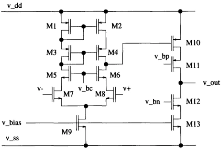
While there is no universally accepted decomposition of op amps, a common way of decomposing a class of op amp topologies is a breakup into an input stage, an output stage, and a compensation module, where the input stage is composed of a current mirror, differential stage, and a current source. Each of the modules can be further decoupled into its constituent interconnected components, such as MOS transistors, capacitors, resistors, voltage biases (sources), and wires. The design process implemented in my system is based on this particular decomposition scheme, shown in Figure 3-1.
The op amps designed by my system's composition scheme are "unbuffered", or OTAs (operational transconductance amplifiers) due to their inability to drive small resistive loads or large capacitive loads. A buffer stage can be added in order to alleviate this problem. I have not included a buffer stage design in my scheme since the primary target application of my op amps is as an integral on-chip sub-system
OP AMP
1
--- -- --- N
I I
Current Differential Current Output Mirror Stage Source Stage
I I
I--- --- - - - -- - - - -- - ---
I
PMOS NMOS Caacitor Voltage Wire
Capacitor Resistor
Transistor Transistor Bias
Figure 3-1: Modular composition of op amps
3.2
Op Amp Topological Template
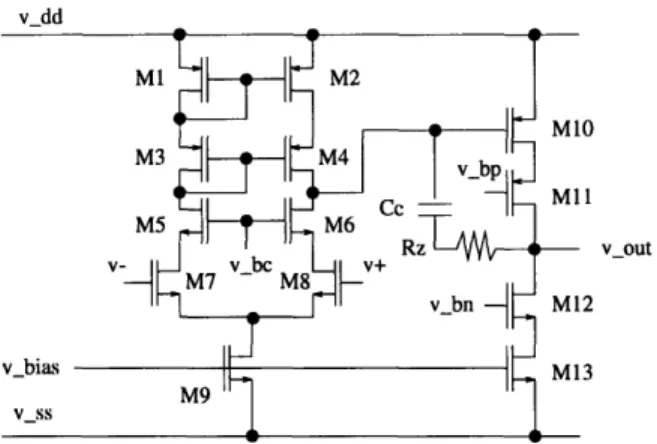
The block-level structure of the op amps that can be designed by our program is given in Figure 3-2.
The first stage of my general op amp topology consists of a differential stage (i.e. a differential input pair), a current source (in fact, a sink), and a current mirror loading module. The first stage provides a differential amplification of the input signals v+ and v_. The single ended output of this stage, Vd, continues into the second,
output stage (a common-source amp with a current sink). The second stage functions
I I I I I I I I I I I I _F I I I
vdd cml4 cm2
'-
0-t
src VSS-Figure 3-2: Topological template for op amps
by the compensation module (a pole-splitting Miller capacitor and an optional zero nulling resistor). The loading of the output is assumed to be purely capacitive, and is represented by the capacitor CL.
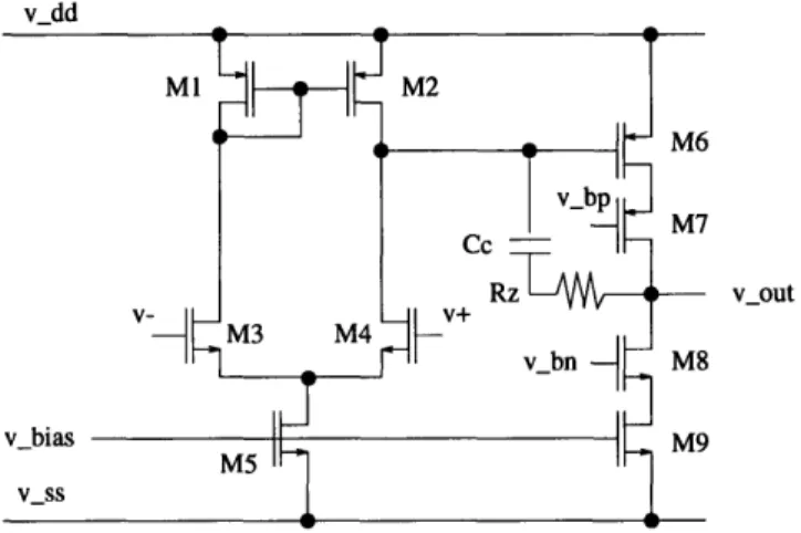
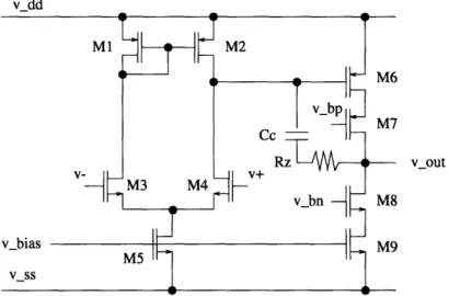
Each of the subcircuit modules in my op amps can be designed in one or more block styles. The module styles are summarized in Figure 3-3. Diagrams of the device-level structure of each particular block style are given in the Appendix.
The only two unorthodox block styles are the nil versions of the output stage and the compensation module. The nil output stage block is composed of a single wire, and it enables my system to design a one stage op amp. The nil compensation
Current Mirror Differential .Qtsoe Output Stage vd v1 - 0 0_ vout . -7 Current Source __ I r . -- A i i -.- C, I I
_
-
fr
I---, r\mmrrnn+; %-I] U0111p~i31SUIVII iCurrent Mirrors Differential Stages Current Sources
Compensation Modules Output Stages
Figure 3-3: Subcircuit styles summary compensation requirements.
While the total number of different op amp topologies that can be designed in my system is 72, they include 16 non-practical topologies which feature a non-nil compensation module with a nil output stage (which shorts out the compensation module and renders it ineffective).
3.2.1
Topology Selection Strategy
The decisions OPASYN undertakes in selecting an op amp topology from its library are based on only two performance requirements: the differential gain and the PSRR. If the gain requirement is larger than some threshold, OPASYN selects a two-stage configuration. Similarly, in case of a stricter PSRR specification, the system chooses a cascoded differential stage topology.
selection is also carried by a set of heuristic rules. Usually, the simplest blocks are selected first. Next, an attempt to design and optimize an op amp satisfying the design requirements is carried out. If the design fails to satisfy the design specifications due to topological shortcomings, a set of heuristic failure rules are invoked and the topology is modified by a replacement of one or more subcircuit blocks with blocks of different style.
However, a successful implementation of good failure and redesign rules is a dif-ficult task. The designer of these rules has to achieve a balanced trade-off between (1) the bias of the rules towards particular topologies for reasons of efficiency, and (2) the ability of the rules to effectively search through the entire topological space. In addition, no matter how well crafted these failure and re-design rules may be, this heuristic strategy could be inefficient due to many possible repeated failures of the designs.
In my system, the structure of the featured genetic optimization algorithm enables a transformation of the topological selection from being a heuristic rule-based selection process to simply being a design parameter in the design optimization phase. My novel approach, detailed in Chapter 5, guarantees a more efficient, exhaustive, and
intrinsically parallel search of the topological design space.
Also, in my opinion, my system features a more effective bias and convergence of the design style towards the best topology to the design problem. The design style convergence in my topologically diverse genetic pool of op amps is biased by natural selection rules which are based on the evaluated performance of each op amp. From generation to a generation, my genetic pool can continue to maintain topological diversity. In comparison, the failure and redesign rules in other automated systems are performed in linear sequential fashion, and may thus introduce unwanted bias in
3.3 Object-Oriented Implementation Approach
My software approach in implementing the hierarchical composition of subcircuit blocks is object-oriented.
The top level of the hierarchy is represented by an op amp object. The op amp module inherits from its five constituent modules. Each of the modules are also objects that are constructed from the six possible circuit components.
To create a particular op amp topology, the genetic algorithm driver (or the user) simply assert
(opamp <opamp-name> <current-mirror> <diff-stage>
<current-source> <output-stage> <compensation>)
which returns an op amp object.
3.3.1 Object Structure
The op amp object, its constituent subcircuit objects, and the circuit component
objects have a similar structure. Each contains the following information:
1. Type/name information
2. Composition/VLSI knowledge 3. Analysis/model knowledge
The type/name information identifies the object and specifies its function. The composition/VLSI knowledge either explicitly details the interconnections between the constituent elements of a subcircuit module or details the physical VLSI makeup of a particular circuit component. For the subcircuit module objects the analy-sis/model knowledge declares the design parameters and features a set of relevant design equations. For the circuit component objects, the analysis/model knowledge
the code for one subcircuit module - the simple differential stage (SDS). Figure 3-5 shows large and small signal circuit diagrams that correspond to the SDS module. The code listings for the remaining subcircuit and component objects are given in the Appendix. (define simple-diff-stage (lambda (m) (case m ;; Type/name information: ((type) 'diff-stage) ((name) 'simple-diff-stage) ;; Composition/VLSI knowledge:
((make) (lambda (model w 1)
(list '(* simple differential stage) ((nmos-tran 'make) 'sdsl 'cml 'vp 'src 'vss model w 1) ((nmos-tran 'make) 'sds2 'cm2 'vn 'src 'vss model w 1) ((wire 'make) 'sdsl 'cm2 'vd)))) ; Analysis/model knowledge: ((params) '(sds-w sds-l)) ((design) '((= ds-area (* 2 sds-w sds-l)) (= v-cm-to-vp (- (vtn 0)) (= v-vp-to-src (+ (sqrt (/ (* 2 ds-i) kn sds-sz)) (vtn 0))) (= ds-gm (gmn sds-sz ds-i kn)) (= sds-gds (gdsn sds-l ds-i)) (= r-vd-to-src (/ sds-gds)) (= sds-w (* sds-sz (leff sds-l ldn))))) (else (error "Unknown message -- simple-diff-stage.")))))
Figure 3-4: Code listing for the simple differential stage object
The composition/VLSI knowledge featured in the subcircuit modules and circuit components provides for the capability of producing a source deck segment for a circuit simulator (written in a SPICE syntax). The top level op amp object not only combines these deck segments, but also adds an appropriate sequence of simulator analysis commands. In op amps containing an inverting non-nil output stage, the op amp object performs a label swap of the input nodes v+ and v_. The automated creation of a simulator source deck interfaces the object composition phase of my
cml cm2 vn I I- -vd vp src src vn VP ds-gm * v-vn-to-src ds-gm * v-vn-to-src
Figure 3-5: Large signal (top) and small signal (bottom) circuit diagrams of the simple differential stage module
optimized designs.
For example, the expression
((nmos-tran 'make)
'sdsl 'cml 'vp 'src 'vss model w 1)
found in the composition/VLSI knowledge list of the object shown in Figure 3-4 constructs one of the differential input stage transistors. Assuming that the model parameter is "5n", the channel width w = 43/um, and the channel length 1 = 10/m, this expression produces the following circuit simulator deck entry:
The analysis/model knowledge of the subcircuit modules and circuit components represented by the set of approximate design and model equations is the basis of the design equations based performance evaluator in my system.
For example, the following equation, taken from the analysis/design knowledge list of design equations of the simple differential stage (SDS) subcircuit object in
Figure 3-4, calculates the active area of that subcircuit:
(= ds-area (* 2 sds-w sds-1))
where ds-area is the total active transistor area, and sds-w and sds-1 are the channel width and length of the two matched devices in the module.
The equation
(= v-cm-to-vp (- (vtn O)))
computes the minimum allowed DC voltage drop between cml (or cm2) and vp nodes in the SDS subcircuit, so that the leftmost NMOS transistor in the subcircuit stays in saturation. The subexpression (vtn 0) computes the threshold voltage of an NMOS transistor assuming a zero source-to-bulk voltage.
The equation
(= v-vp-to-src (+ (sqrt (/ (* 2 ds-i) kn sds-sz)) (vtn 0)))
calculates the minimal DC voltage drop between nodes vp and src such that the leftmost NMOS transistor remains in the saturation region. The variable ds-i is the DC bias current flowing through each of the branches of the SDS subcircuit, kn is the transconductance parameter for NMOS transistors, and sds-sz is the size of each of the transistors in the SDS module.
The equations
(= ds-gm (gmn sds-sz ds-i kn)) (= sds-gds (gdsn sds-1 ds-i))
compute the small signal stage transconductance ds-gm, the small signal device con-ductance sds-gds, and small signal resistance r-vd-to-src of the rightmost tran-sistor in the stage. The subexpressions (gmn ... ) and (gdsn ... ) are recursively expanded by the equation solver into the following model equations:
(= (gmn w/l id kn) (sqrt (* 2 kn id w/l)))
(= (gdsn 1 id) (* (lambdan 1) id))
(= (lambdan 1) (* lambdan-maw (/ (leff min-active-width ldn)
(leff 1 ldn)))) (= (leff 1 d) (- 1 (* 2 d)))
where the subexpression (lambda ... ) computes the channel-length modulation parameter, while (leff ... ) calculates the effective channel width.
Finally, the equation
(= sds-w (* sds-sz (leff sds-l ldn)))
computes the actual channel width of the two devices in the SDS subcircuit.
The techniques I use to transform the design equations by subexpression expan-sions, and the methods I use to solve the design equations are discussed in Chapter 4.
Chapter 4
Op Amp Performance Evaluation
The objective of a circuit performance evaluator is to compute various performance functions from the set of design parameters as shown in Figure 4-1. Many of the performance functions for my op amps are non-linear functions of the design parame-ters, and can be accurately determined only by a circuit simulation. My system thus features two op amp performance evaluators: an approximate design equation based evaluator, and a simulator based evaluator.
4.1 Approximate Design Equation Performance
Evaluator
The approximate design equation performance evaluator is based on the set of first order analytic design equations that are asserted from the top-level op amp object, its constituent subcircuit modules, and the circuit components featured in the design. These equations express approximate functional dependencies of the performances of the op amp on the design parameters.
The primary advantage of my approximate equations based evaluator is its much greater computing speed when compared to a simulator based scheme. In addition,
Design
parameters Performance functions Transistor sizes Voltage biases Compensation capacitor Nulling resistor Active area DC power Input voltage CMRs Output voltage swings Output resistance Differential gain CMRRUnity gain bandwidth Phase margin
PSRRs
Slew rate
Figure 4-1: Op amp performance evaluation
search direction in the parameter space. However, when an equations based op amp evaluator is used with any optimization method, the achieved designs are in fact only near-optimal due to the approximate nature of evaluating the designs.
The process of creating the design equations (the knowledge base) for each subcir-cuit module in my modular composition scheme is significantly less time consuming that when all design equations for a fixed circuit topology are mixed with the language that manipulates that knowledge in a single computer program.
The design equations in my evaluator are solved by a mixture of symbolic algebraic transformations, and numerical methods. The balanced mix of symbolic transforma-tions and numerical computatransforma-tions allows full freedom in using highly non-linear
equa-Op Amp
Performance Evaluator
---in the CIROP system [23]. An ability to handle a variety of non-l---inear equations is particularly important in the approximate analysis based design of MOS analog circuits compared to bipolar analog circuits.
4.1.1
Design Equations
Each object in my hierarchical composition scheme contains relevant design equations which represent the analysis/model knowledge associated with that object.
Typically, the higher the object in the hierarchy, the more general and high level the design equation asserted by that object. For example, among the design equations asserted by the top-level op amp object are the equations used to determine the DC power dissipation of a two stage op amp:
(= dc-power (* (+ cs-i os-i) (- vdd vss))
where cs-i and os-i are the DC bias currents flowing through the current source and output stage. In case the op amp consists of only one stage, the nil-output-stage object asserts the equation (= os-i 0).
The op amp object asserts almost all of the high level equations that compute the performance of the op amp. In some instances, however, the structure of the equation is influenced by the choice (or a combination of choices) of the constituent subcircuit modules, and equation-switching information needs to be propagated upward - from the subcircuit module level to the op amp object. Here is, for example, the equation which computes the slew rate:
(= slew-rate
(if (and compensation? output-stage?)
(/ cs-i cc)
(if (and (not compensation?) output-stage?) (/ os-i c-ii)
(/ cs-i c-i))))
The variables cc, c-i, and c-ii are the compensation capacitance, and the loading capacitances of the first and the second stage respectively. For example, for a nil output stage, c-i is equal to the output load capacitance cl and c-ii is non-existent; for a non-nil output stage, c-i is equal to the gate-to-source capacitance of the common-source device and c-ii is equal to to the output load capacitance cl.
An alternative to the equation-switching strategy is to leave the assertion of the equations to the subcircuit modules. This is possible as long as it is one single sub-circuit choice, and not a combination of choices that forces a change in the structure of the equation. For example, the DC PSRR (power supply rejection ratio) equations differ with respect to the choice of the utilized output stage. This approach does not require use of boolean signals, but is less elegant since it causes the assertion of a high level equation to be done from a less visible lower level of hierarchy.
At the middle level of hierarchy, the subcircuit objects assert equations that com-pute various properties of the modules, such as voltage drops, currents, transcon-ductances, and output resistances. For example, the simple-output-stage object asserts an equation that specifies the DC bias stage current os-i:
(= os-i (idn-sat sos-sz2 (- vbias vss) 0 kn))
where idn-sat computes the DC saturation MOS transistor current given the size
sos-sz2 of the MOS device, the gate to source voltage (- vbias vss), a zero source
to bulk voltage 0 and the transconductance parameter kn.
Most of the equations associated with the frequency domain behavior of the op amps are asserted by the compensation modules. In particular, these equations in-clude a complex domain transfer function equation, along with equations for the poles and zeros, and the phase margin. This is understandable since it is the compensation module choice that drastically changes the algebraic structure of the transfer function. The circuit components, located at the bottom of the hierarchy, assert basic large