Diamond Nanophotonic Devices for Quantum
Information Processing and Sensing
by
Luozhou Li
Submitted to the Department of Electrical Engineering and Computer
Science
in partial fulfillment of the requirements for the degree of
Doctor of Philosophy
at the
MASSACHUSETTS INSTITUTE OF TECHNOLOGY
September 2015
ARCHMVS
MASSACHUSETTS INSTITUTE OF TECHNOLOGYNOV 0
22015
LIBRARIES
@
Massachusetts Institute of Technology 2015. All rights reserved.
Author ...
Signature redacted
Department of Electrical Engineering and Computer Science
August 21, 2015
Certified by...
Signature redacted
Dirk Englund
Jamieson Career Development P ofessor f Electrical Engineering and
Computer Science
Thesis Supervisor
Accepted by ...
Signature redacted
/Proffk4JLeslie
A. Kolodziejski
Chairman, Department Committee on Graduate Theses
Diamond Nanophotonic Devices for Quantum Information
Processing and Sensing
by
Luozhou Li
Submitted to the Department of Electrical Engineering and Computer Science on August 21, 2015, in partial fulfillment of the
requirements for the degree of Doctor of Philosophy
Abstract
The nitrogen vacancy (NV) center in diamond has in recent years emerged as a promis-ing solid state system for quantum information processpromis-ing and senspromis-ing applications. However, using NV centers to build up quantum networks for these applications faces several challenges, such as the lack of efficient interface between NVs and photons, difficulty of maintaining spin coherence times, and scalable techniques for fabrication of NV-photon networks. This thesis focuses on overcoming these challenges by fab-ricating diamond devices to improve the collection efficiency of NV photon emission, especially from the zero phonon line (ZPL), while maintaining long spin coherence times after fabrication.
After an introduction to the subject matter in Chapter 1, Chapter 2 discusses a fabrication technique to produce vertical membranes out of bulk diamond plates. This work showed that after reactive ion etching, the spin properties of isolated NVs in diamond nanostructures were largely preserved. We also observed increased pho-toluminescence collection from shallow implanted NV centers in these slabs.
In Chapter 3, we describe a versatile nanofabrication method based on re-usable silicon membrane hard masks, patterned using standard lithography and mature sili-con processing technology. These masks are transferred precisely onto targeted regions of diamond membranes, where photonic devices can be realized without the need for spin coating, wet etching or electron beam exposure.
Chapter 4 describes and demonstrates an alternative technique for fabricating one-dimensional photonic crystal (PC) cavities in single-crystal diamond by a com-bination of reactive ion etching (RIE) and focused ion beam milling. We compare it to transferred silicon hard mask lithography with RIE.
Chapter 5 demonstrate NV-nanocavity systems in the strong Purcell regime with consistently high Q factors while preserving the long spin coherence times of NVs. These systems enable coherent spin control of cavity-coupled semiconductor qubits with coherence times exceeding 200 s - an increase by two orders of magnitude over previously reported optical cavity-coupled solid-state qubits.
Chapter 6 introduces a circular diamond "bullseye" grating that achieves the high-est reported photon collection rate from a single NV center of 4.56 0.08 Mcps at
saturation when fitted with the widely-used background counts subtraction method. We also quantified the emission by a g(2 -corrected saturation curve measurement which gives a rigorous single photon count rate of 2.7 0.09 Mcps. By using
dynam-ical decoupling sequences, we measured a spin coherence time of 1.7 t 0.1 ms, which is comparable to the highest reported spin coherence times of NVs under ambient conditions and also indicates that the bullseye fabrication process does not degrade the spin properties noticeably. The planar architecture allows for on-chip integration, and the circular symmetry supports left- and right-handed circularly polarized light for spin-photon entanglement.
In Chapter 7, we demonstrate a top-down fabrication process using a porous metal mask and a self-guiding RIE process that enables rapid nanocrystal creation across the entirety of a high-quality chemical vapor deposited (CVD) diamond substrate. High-purity CVD nanocrystals produced in this manner exhibit single NV phase coherence times reaching 210 ps and magnetic field sensitivities of 290 nT.Hz-1/2 without compromising the spatial resolution of a nanoscale probe.
Thesis Supervisor: Dirk Englund
Title: Jamieson Career Development Professor of Electrical Engineering and Com-puter Science
Acknowledgments
Throughout the course of my time at Massachusetts Institute of Technology (MIT)
and Columbia University, numerous individuals guided, helped, assisted and encour-aged me along the path. Below is an incomplete list of those generous people and mentors.
First and foremost, I would like to thank my advisor Professor Dirk Englund for his guidance and support. Dirk invested a lot of time in meeting and mentoring me, every time bursting with new ideas, while still providing me the freedom to try my own ideas and to collaborate with people. He had huge patience towards improving my writing skills and practicing talks for conferences. I have worked with Dirk from the very beginning of his group with only him and me to now, over 20 researchers. I feel grateful to have been part of this process and to have had an advisor with so much knowledge, patience, and concern for his students. In his lab I was fortunate to be exposed to a wide variety of advanced experimental methods and have hands-on experience in state-of-the-art fabrication and characterization techniques. I thank
him for allowing me to navigate through the sometimes very challenging waters of
experimental research while helping me to stay on course for discovery. From him, I have learned to become a better presenter, writer, scientist, leader, and person.
I would like to thank Professors Karl Berggren and Terry Orlando for assisting
me through my time at MIT. It is my great honor to have them in my doctoral committee. Prof. Berggren is a leading expert in nanofabrication. I have learned a lot of nanofabrication techniques from his publications and his group. Prof. Orlando is a leading expert and pioneer in quantum information science, and I thank him for his patience and mentorship. In addition, I would like to thank my graduate counselor, Professor Jeff Lang, who allowed me to seek advice and never be turned down.
I would also like to acknowledge our collaboration with Columbia University,
Brookhaven National Laboratory (BNL) and beyond. First, my deep gratitude to our collaborator Professor Richard Osgood, who carefully revised my first paper and
helped monitor the whole process. Special thanks go to our collaborators from BNL nanofabrication experts, namely to Dr. Ming Lu, Dr. Aaron Stein, Dr. Fernando Camino, Dr. Chang-Yong Nam, Dr. Mingzhao Liu, and Dr. Chuck Black. I would like to thank Dr. Mircea Cotlet for his advice and for his help on confocal
mea-surements at BNL. In addition, my deep gratitude to the ion implantation team at Albany State University led by Professor Hassaram Bakhru. And I would like to thank Dr. Matthew Markham and Dr. Daniel Twitchen from Element Six for offering world-leading diamond membrane samples.
I thank the entire Englund group members (past and present) for the support and
comradeship. I thank people in the diamond subgroup, including in particular Dr. Jonathan Hodges, Dr. Ophir Gaathon, Dr. Igal Bayn, Dr. Tim Schr6der, Dr. Florian Dolde, Dr. Sinan Karaveli, Edward Chen, Matthew Trusheim, Hannah Clevenson, Jiabao Zheng, Michael Walsh, Sara Moudirain, Christopher Foy, Donggyu Kim, Ben Lienhard, Hyeongrak Choi, Reyu Sakakibara, Noel Wan, and Rish Patel. Especially, I would like to acknowledge two members of the group with whom I had the closest interaction with: Dr. Tim Schr6der and Edward Chen. I have learned tremendously from both of you. Your insight, creativity and work ethics are truly admirable. Thank you for your encouragement and our friendship.
Finally, I thank Mark Mondol and James Delay from the NSL cleanroom, as well as Kurt Broderick from EML and Vicky Diadiuk from MTL, who helped me a lot on developing fabrication processes at MIT. And I would like to thank MIT Writing and
Communication Center, especially Elizabeth Fox (Betsy), for the assistance and help on improving my English writing skills.
Contents
1 Introduction
1.1 Quantum information processing (QIP)
1.2 Nitrogen Vacancy (NV) Centers . . . .
1.3 Challenges using NVs for QIP and sensing
1.4 Thesis Overview . . . .
1.5 Relevant publications . . . .
2 Diamond membrane fabrication
2.1 Introduction . . . .
2.2 Experiments . . . .
2.3 Material properties of diamond nanoslabs . . . .
2.4 Spectral properties of NV centers in diamond nanoslabs .
2.5 Conclusion and Outlook . . . .
3 Transferred hard mask lithography
3.1 Introduction . . . .
3.2 Two methods for silicon mask transfer . . . .
3.3 Silicon masks for etching . . . .
3.4 D ry lift-off . . . .
3.5 D iscussion . . . .
4 One-dimensional photonic crystal cavities in single-crystal diamond
4.1 Introduction . . . . 23 . . . . 23 . . . . 23 . . . . 25 . . . . 26 . . . . 27 29 29 30 36 41 44 45 . . . . 45 . . . . 47 . . . . 50 53 . . . . 55 57 57
4.2 RIE-FIB approach . . . . 58
4.3 Silicon mask approach . . . . 60
4.4 Results and Discussion . . . . 63
4.5 C onclusion . . . . 65
5 Coherent spin control of nanocavity-enhanced NV qubits in dia-mond 67 5.1 Introduction . . . . 68
5.2 Simulations . . . . 70
5.3 Nanofabrication using silicon masks . . . . 70
5.4 Optical measurements and cavity tuning . . . . 73
5.5 Spin properties of nanocavity-coupled NVs . . . . 81
5.6 D iscussion . . . . 81
6 Bullseye circular gratings to enhance broadband NV photolumines-cence collection efficiency 85 6.1 Introduction . . . . 85
6.2 D esign . . . . 86
6.3 Fabrication . . . . 87
6.4 Optical characterization . . . . 88
6.5 NV photon count rate estimation . . . . 89
6.6 Spin properties of NVs inside the bullseye . . . . 93
6.7 D iscussion . . . . 94
7 Scalable fabrication of high purity diamond nanocrystals with long-spin-coherence nitrogen vacancy centers 95 7.1 Introduction . . . . 95
7.2 Fabrication procedure . . . . 96
7.3 Optical and spin characterization . . . . 100
8 Summary and Outlook 103
8.1 Diamond nanoslab fabrication ... 103
8.2 Transferred hard mask lithography . . . . 103 8.3 Photonic crystal cavities for coherent spin control of NV qubits . . . 104 8.4 Circular bullseye gratings . . . . 105 8.5 Long-coherence diamond nanocrystals . . . . 105
List of Figures
1-1 Confocal fluorescence image of NV centers in diamond, which was ob-tained by scanning the sample over the laser spot of a confocal
micro-scope. ... ... 24
1-2 Fluorescence spectrum of a single NV. Note the presence of Raman line at 572 nm, the zero phonon line (ZPL) at ~ 637 nm, and phonon sideband (PSB) when the 532-nm laser is focused on the NV. .... 25
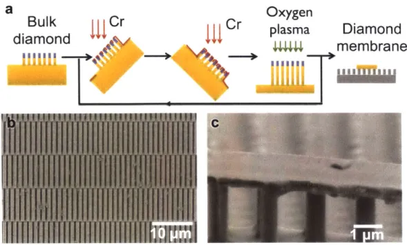
2-1 Detailed diamond membrane fabrication procedure using RIE. (a) HSQ spin coating; (b) electron beam lithography and development; (c) ini-tial oxygen plasma etching of diamond; (d) and (e) Cr deposition at an oblique angle; (f) continued oxygen plasma etching of diamond; (g) me-chanically separated diamond nano-slabs from diamond; (h) diamond
nano-slabs transferred to a patterned silicon substrate; (i) if necessary, further thinning of diamond nano-slabs with oxygen or chlorine plasma etching. . . . . 31
2-2 Diamond membrane fabricated using RIE. (a) This process alternates between oxygen plasma etching and Cr mask deposition steps and re-sults in a high-aspect-ratio diamond membrane. (b) Diamond mem-brane (top view) stands vertically on a bulk diamond sample before mechanical separation. (c) Diamond membrane (side view) is trans-ferred onto a patterned silicon substrate. . . . . 32
2-3 Diamond membrane fabrication procedure using FIB. (a) Diamond membrane (side view), resulting from an FIB cut, is picked up from a bulk diamond sample and placed near a TEM grid. The inset shows a top view of the same diamond membrane after two 6 tm-deep trenches were then milled into both sides of the membrane. (b) Expanded view of a sample bonded to a TEM grid. (c) Diamond sample after FIB
thinning of a region, denoted by the black ellipse, to a thickness of less than 100nm for HRTEM imaging. . . . . 34
2-4 Raman spectra from a pristine CVD diamond (curve shown in blue), FIB-processed diamond (curve shown in green), and RIE-processed diamond (curve shown in red). FIB-processed diamond shows a broad-background Raman feature surrounding the Raman line. . . . . 35
2-5 TEM investigation of FIB- and RIE-processed diamond membranes. Low-magnification TEM images are taken from (a) FIB- and (b) RIE-processed diamond membranes with electron diffraction patterns (in-set). HRTEM images are taken from (c) FIB- and (d) RIE-processed diamond membranes. (c) is the expanded view of the edge of black ellipse region in (a) to show the near-surface interface between amor-phous and crystalline diamond. (d) is the expanded view of the black
rectangular region of (b) to show diamond crystal without any visible damage with atomic resolution. . . . . 38
2-6 Images of exfoliated nanoslabs. Slabs are removed from the bulk dia-mond substrate by abrasion with a hypodermic syringe and transferred to a glass slide (a) using a PDMS stamping technique. The diamond slabs did not show characteristic bright spots, indicative of NVs, at first. Repeated implantation and annealing caused an accumulation of NVs inside the slabs. The sample is then scanned over the laser spot of a confocal microscope to obtain a fluorescence image (b). . . . . . 40
2-7 Fluorescence spectrum of a single NV in a nanoslab attached to the bulk. Note the presence of the ZPL at 637 nm and PSB from 650 nm to 800 nm when the optical excitation is focused on the NV. . . . . . 42
2-8 Second-order autocorrelation function (g(2) (T)) of the emitted photons as measured in a Hanbury-Brown-Twiss configuration. Note that the
g(2
)(0) value falls well below jg(2
)(T -+ oc), indicating a single emitter. 43
2-9 Diamond membrane fabricated with PCs using FIB (top view). Un-fortunately spectroscopy measurements did not give us any cavity res-onance. We attributed the reason for no found resonance to the the FIB surface damage. . . . . 44
3-1 Mask production and micro-PDMS transfer technique. (a) Arrays of free-standing silicon masks on an SOI wafer. Inset: Scanning electron micrograph (SEM) of a typical suspended silicon mask using
250-nm-wide, 500-nm-long bridges connected to the substrate. The bridges are denoted by white circles. (b) A micro-PDMS adhesive attached to a tungsten probe tip (sideview) for transfer of a silicon hard mask. (c) Illustration of a silicon mask attached to the micro-PDMS adhesive on a tungsten tip during the transfer. (d) A silicon mask attached to the micro-PDMS adhesive on a tungsten tip in air (bottom view). The silicon mask is circled by a blue dotted line. . . . . 48
3-2 Millimeter-scale masks were transferred onto a piece of quartz using a polytetrafluoroethylene (PTFE) sheet. . . . . 50
3-3 Illustration of patterning a diamond membrane with a silicon mem-brane as an etch mask. (I) A patterned silicon mask was transferred onto a diamond membrane (less than 300 nm in thickness, adhering to a bulk silicon substrate) using a micro-PDMS adhesive. (II) The silicon membrane on top of the diamond membrane served as an etch mask for oxygen plasma etching. (III) The diamond membrane was
patterned with nanostructures during oxygen etching after subsequent mask removal. (IV) An SF6 isotropic dry etching removed the
sili-con underneath and suspended the diamond membrane at the devices' locations. . . . . 51
3-4 (a) Optical image of a silicon mask covering a diamond membrane that is circled by the blue dotted line. (b) SEM of a suspended diamond L7
PC cavity. Inset: Measured cavity resonance (blue dots) at 623.3 nm
with a Lorentzian fit, yielding a
Q
factor of 4,700 (red line). . . . . . 513-5 Quality of diamond dry etching using silicon masks. (a) Pattern trans-fer from silicon masks onto diamond membranes with vertical sidewalls.
(b) Oxygen reactive ion etching of bulk diamond with silicon masks.
The etch depth was 8.5 ltm. The image was taken when the sample was tilted at 800. We found no visible change in the mask thickness. . 53
3-6 Illustration of dry lift-off: (I) A patterned silicon mask was transferred onto the substrate. (II) A metal layer was deposited via an electron beam or thermal evaporation. (III) A tungsten tip was swept across a silicon mask to mechanically remove the mask. . . . . 54
3-7 (a) SEM image of a nanoscale pattern. (b) Expanded view of the white rectangular region in (b). The minimum linewidth that we achieved w as 10 nm . . . . . 54
3-8 Patterning on a fiber facet. (a) A silicon membrane with patterned gold dot arrays was transferred onto a fiber facet using a micro-PDMS adhe-sive. Inset: Expanded view of the silicon membrane on the fiber core.
(b) After silicon mask transfer, gold dot arrays were tone-reversely
patterned on a fiber facet by deposition of a layer of 70-nm gold and removal of silicon masks using a tungsten tip. Inset: Expanded view of the white rectangular region to show gold dots on the fiber facet. . 55
4-1 Illustration of RIE transferring the patterns from HSQ into bulk dia-mond and FIB cutting the bottom to suspend the nanobeams. . . . 58
4-2 Cavity fabrication in bulk diamond using RIE-FIB. (a) The cross sec-tion of RIE-etched nanobeams shows straight sidewalls for the first 400 nm of etching into the diamond. The top surface is coated with Cr to prevent charging during FIB cutting. (b) SEM of a representative nanobeam cavity (I) after RIE, (II) after FIB milling of the bottom di-amond, and (III) after annealing at 1,000 'C for 2 hours in vacuum. (c)
SEM of the same nanobeam cavity as in (c) after annealing at 1,000 'C
4-3 Illustration of patterning on a diamond membrane using a silicon mem-brane as an etch mask: (a) NVs were created - 100 nm below the 5- Lm diamond membrane surface by implantation of 15N atoms. The dia-mond was subsequently annealed at 850 'C. (b) The 5-jLrm diadia-mond membrane was flipped over on a silicon substrate and thinned by RIE to ~ 200-nm thickness. (c) A patterned silicon mask was transferred
onto a diamond membrane (less than 300 nm in thickness, adhering to a bulk silicon substrate) using a micro-PDMS adhesive. (d) The silicon membrane on top of the diamond membrane served as an etch mask for oxygen plasma etching. (e) The diamond membrane was patterned with nanostructures during oxygen etching after subsequent mask re-moval. (f) An SF6 isotropic dry etching removed the silicon underneath
and suspended the diamond membrane at device locations. . . . . . 60
4-4 SEM of 200-nm diamond memrbanes. . . . . 61
4-5 SEMs of one-dimensional PC cavities produced by silicon mask method. (a) Side view and (b) top view of an array of one-dimensional PC cavities with rectangular holes. (c) A close-up image of a single one-dimensional PC cavity with rectangular holes. (d) Top view and (e) side view of an array of one-dimensional PC cavities with circular holes. 62
4-6 Optical characterization of one-dimensional PC cavities with circular holes. (a) Measured cavity resonance (black dots) with a quality factor
Q
~ 1, 710 from a Lorentzian fit (blue line). (b) The spectrum taken at low temperature from a different sample with a Raman line at 573 nm, NV0 ZPL at 575 nm, NV- ZPL at 637 nm, and three cavity resonance peaks at 614 nm, 688 rn, and 741 nm. Inset: normalized second-order auto-correlation measurement with g(2) (0) = 0.378 for the
5-1 On-chip NV-nanocavity system in diamond. a, The diamond PC
cavi-ties are integrated on a silicon substrate with metallic striplines for co-herent spin control and optically addressed using a confocal setup with 532-nm CW excitation and photoluminescence collected > 630 nm.
The inset shows the NV-nanocavity system with g the NV-nanocavity Rabi frequency, -y the NV natural spontaneous emission (SE) decay rate, and i the cavity intensity decay rate. The NV consists of a
sub-stitutional nitrogen atom adjacent to a vacancy in the diamond lattice.
I, denotes the current through the stripline, and h the PC thickness.
b, Simulated electric field energy density for the optimized
fundamen-tal cavity mode. The PC has a width W and a lattice constant varying from 0.9a at the center to a = 220 nm over five periods. c, SEM of a representative cavity structure. The scale bar represents 1 pLm. d, Measured cavity resonance (dots) with a quality factor
Q
- 9, 900 200 from a Lorentzian fit (blue line). . . . . 695-2 FDTD simulation. a, Structural parameters. a denotes the lattice constant, w the beam width, h the thickness, h, the hole width, and hy the hole length. b, Illustration of the linear cavity lattice constant profile, which defines the potential well. c, Cavity Q/Vmode as the hole widths and lengths are varied. The sweep parameter hy was limited to below 2a to avoid multimode operation along the y-direction. . . . . . 70
5-3 Fabrication procedure (left column) and SEM of representative struc-tures (right column). a, NVs were created ~100 nm below the surface
of the diamond membranes by implantation of 15N atoms and sub-sequent annealing at 850 0
C. Right: SEM of 200 nm membrane. b,
Silicon masks were patterned on SOI, released, and transferred onto diamond membranes. Right: Patterned silicon mask before transfer. The scale bar represents 1 tm. c, Oxygen RIE was used to pattern
dia-mond membranes. Right: The false-color SEM shows the silicon mask (purple) on diamond after oxygen etching. The scale bar represents 1
im. d, Patterned diamond membrane on microwave striplines for op-tical and spin characterization. Right: SEM of diamond PC structures above metallic striplines in silicon channels. The scale bar represents
5 m. e, Distribution of cavity
Q
factors from one fabrication run.78 (blue bars) of 83 cavities showed resonances in the range of 600-800 nm, while five (red bar) showed no resonances in this wavelength
range. The mean
Q
is 6,200. . . . . 715-4 (a) SEM of the diamond devices integrated with the microwave archi-tecture. (b) Close-up SEM of the diamond photonic crystals on top of m icrowave striplines. . . . . 73
5-5 Optical characterization of NV-nanocavity system A. a, Photolumines-cence confocal image of diamond PC structures. The scale bar is 5 Lm. Single NVs are identified by circular white spots. System A: The dot-ted red circle shows a single NV close to the cavity center (indicadot-ted by the blue dotted line). Inset: Normalized second-order auto-correlation measurement with g(2)(0) = 0.28. b, Gas tuning of system A. The
logarithmic plot shows the cavity resonance and two strain-split ZPL branches from a single NV (EY and E2, 2A = 286 GHz). As the gas condensation red-shifts the cavity resonance, it sequentially enhances the two ZPL branches. The inset shows the intensity of the E. ZPL transition as a function of cavity detuning. This curve follows the expected Lorentzian dependence of the Purcell enhancement given by Eqn. 5.1 and shows that the cavity
Q
factor remains constant through-out the tuning process. c, Spectra of system A in the uncoupled (I) and coupled cases with Ac, = AEy (II) and cav = AE. (III). Note the difference in scaling between E_ and E. cases. The black lines are Lorentzian fits to the data, yieldingQ
= 1,700 t 300 for the cavity. 745-6 NV energy level model. . . . . 78
5-7 Optical characterization of NV-nanocavity system B. a, System B at
maximum Purcell enhancement. The inset shows a close-up of the spectrum. The ZPL transitions of four individual NVs (including the cavity-coupled ZPL) are visible, each with a different strain-induced spectral position. The accumulated phonon sidebands of these NVs are also apparent. b, High resolution spectra of system B in cavity-coupled and uncavity-coupled cases, respectively. The insets show the lifetime measurements corresponding to r = 6.7 ns and Trff = 18.4 ns. . . . 79
6-1 (a) Illustration of an array of diamond bullseye gratings adjacent to a microwave (MW) strip line. (b) Schematic of the circular grating. a
denotes the lattice constant and gap the air spacing between circular gratings. (c) Simulated electric field intensity (log scale) in the x = 0
plane with air above and glass below the diamond. A dipole emitter was placed in the center of the bullseye grating, and was oriented along
the horizontal direction. . . . . 86
6-2 (a) Scanning electron micrograph and (b) PL scan of an NV within a diamond bullseye grating (system A). . . . . 87
6-3 (a). Spectrum of an NV inside the bullseye grating. (b) Convolution of standard NV spectrum (pink) with a simulated, wavelength-dependent collection efficiency (blue). . . . . 88
6-4 a-d: Simulated and experimental back-focal-plane images. The con-centric circles are in units of numerical aperture, and the color
inten-sities for all four images are normalized to their respective maximum intensity value for wavelengths from 640 - 650 nm for the same E, po-larization (pointing left-right). Measured far-field emission pattern of an NV in the ~300 nm thick diamond membrane with (a) and without
(c) a grating structure. Simulated far-field emission pattern of a dipole
oriented along the horizontal direction inside a membrane with (b) and
6-5 (a) The saturation curves of the bullseye-enhanced single NV in system
A. The red curve is a fit to data with background counts subtracted,
and asymptotically approaches 3.27 0.37 Mcps at a saturation
exci-tation power of 77 30 pW. The blue curve is a fit to g(2
)-corrected counts (for details, see main text), and asymptotically approaches 2.41 0.2 Mcps at a saturation excitation power of 84 30 LW. The
second-order auto-correlation measurement (inset) indicates a
mini-mum g(2
) (0) = 0.320 0.005 at 10 1W. (b) Characterization of system
B. The red curve is a fit to data with background counts subtracted, and asymptotically approaches 4.56 0.08 Mcps at a saturation
exci-tation power of 255 20 pW. The blue curve is a fit to g(2)-corrected counts, and asymptotically approaches 2.70+0.09 Mcps at a saturation excitation power of 150 16 pW. The second-order auto-correlation
measurement (inset) indicates a minimum g(2
)(0) = 0.279 0.003 at 10 W . . . . . 9 1
6-6 (a) Saturation curve analysis of the bullseye-enhanced single NV in system B. The green curve is a fit to the total count rate, which asymp-totically approaches 4.38 0.3 Mcps at a saturation excitation power
of 288 30 kW with the linear background term a = 2215 t 200
counts/W given a fitting function C(P) =
-
+ aP. The bluecurve is a linear fit to background counts measured ~600 nm away
with a = 2100 t 100 counts/ . . . . 93
7-1 Process schematic. (a) Bulk diamond is masked by sputter-coated AuPd. (b) 02 inductively coupled plasma etches the diamond with the AuPd as a mask. (c) As the etch continues, the AuPd is completely removed. (d) The diamond is implanted with nitrogen, annealed, and chemically treated to form NV centers. (e) The CVD nanodiamonds are mechanically removed from bulk and (f) transferred onto glass cov-erslips for confocal microscopy . . . . . 97
7-2 Scanning electron micrographs. (a) AuPd mask. (b) Sideview and (c) top-view of nanocrystals attached to bulk diamond. (d) Nanocrystals separated from bulk and transferred onto a silicon substrate. . . . . . 99
7-3 Optical characterization. (a) Scanning confocal image of CVD nanodi-amonds on glass. The fluorescence from a single NV is indicated by the red square. (b) Spectrum of a single NV center in a CVD diamond nanocrystal showing the NV ZPL at 638 nm. (c) Second-order auto-correlation function of NV photoluminescence indicating single-emitter
behavior with g(2
)(0) < 0.5. Blue line: fit to function 1 + AeI(t/T) with
Chapter 1
Introduction
1.1
Quantum information processing (QIP)
The field of quantum information processing (QIP) takes advantage of the proper-ties of quantum mechanics to perform tasks that have no known solutions in classi-cal physics [1], including exponentially faster computational algorithms [2, 3], long-distance quantum state teleportation [4, 5], and efficient simulation of many-body quantum systems [6, 71. A central aim of QIP is the ability to create efficient quan-tum entanglement among a large number of quanquan-tum memories that are individually addressable. This entanglement can be created through atom-photon interactions, allowing the establishment of quantum networks [8]. Quantum networks require suf-ficiently spaced, long lived quantum memories as stationary qubits and photons as flying qubits for the information transfer. There is strong interest in solid-state imple-mentations for scalability, stability, and device integration [91, which is now becoming possible using nanofabrication techniques that were developed in the semiconductor industry over the past decades.
1.2
Nitrogen Vacancy (NV) Centers
Among solid-state quantum bits (qubits), the negatively charged nitrogen vacancy
F
112x 10, 2 10 4 8 6 6 8 10 12 E2 8 10 12 14 16 18Figure 1-1: Confocal fluorescence image of NV centers in diamond, which was ob-tained by scanning the sample over the laser spot of a confocal microscope.
NV center consists of a nitrogen atom adjacent to a vacancy in the diamond lattice.
Not only NV centers exist in natural diamond, but also they can be produced in artificial diamond either during the chemical vapor deposition growth process [11] or
by nitrogen ion implantation and subsequent annealing [12]. Excited by the green
laser, it is fluorescent in red (See Figure 1-1 for the confocal fluorescence scan of typical
NV centers). It has a zero phonon line (ZPL) at ~ 637 nm and broad phonon sideband
(PSB) ranging from 650 nm to 800 nm (Figure 1-2). Spin-selective optical transitions
allow individual NV electron spins to be easily observed using standard confocal microscopy through optically detected magnetic resonance (ODMR) [131. In the simplified energy level diagram of NVs, we consider three different electronic states, one ground state, one excited state and one metastable state. The NV ground state has an associated spin triplet. The energy difference between associated magnetic sublevels m, = 0 and m, = 1 states is ~2.88 GHz. The degeneracy of m, = 1
states can be lifted by an external magnetic field via inducing a Zeeman shift [141. One can employ two sub-levels of the triplet to encode a qubit. Because of the nearly spin-free carbon lattice and weak spin-lattice interactions, these electronic ground states have extremely long coherence [15].
1800- 1600- 1400-1200 - 1000- 800-60 50 600 650 700 750 wavelength (nm)
Figure 1-2: Fluorescence spectrum of a single NV. Note the presence of Raman line at 572 nm, the zero phonon line (ZPL) at - 637 nm, and phonon sideband (PSB) when the 532-nm laser is focused on the NV.
and readout [16, 171, and long spin coherence times [15], NV centers have an ineffi-cient spin-photon quantum interface due to two reasons. First, the overall collection efficiency of the NV is low due to high index contrast of the diamond-air interface. Second, the NV has a small Debye Waller factor (the ratio of emission into the ZPL over both ZPL and phonon sideband) with only ~ 1-3% of photons emitted into the ZPL transition [18]. For optical entanglement of two NVs, the photon emission needs to be a coherent process, i.e., the photons must be emitted in the ZPL. The inefficient interface between NV qubits and optical photons causes low entanglement generation rate [19J.
1.3
Challenges using NVs for QIP and sensing
Using NVs to build up quantum networks for QIP and sensing presents three main challenges:
1. We lack an efficient interface between NV qubits and optical photons.
Re-cently quantum entanglement [19] and teleportation [201 have been achieved between two NV memories, but the entanglement generation rate is low, about
one entangled photon pair per several minutes, which prevents scaling the en-tanglement to more qubits. Only 3% useful photons are emitted through ZPL for the above-mentioned entanglement protocol, and the high refractive index of diamond prevents photons from being collected through an objective lens. A
more efficient NV-photon interface [21] is needed for faster QIP.
2. It is difficult to maintain spin coherence times for quantum computation after device nanofabrication. Diamond nanostructures and nanocrystals with long spin coherence times are desired for quantum information and sensing appli-cations, but the production method may introduce paramagnetic impurities or lattice damage that limit the spin coherence times of NV centers [22, 231.
3. It is desirable to scalably fabricate individual quantum nodes in diamond and
integrate these nodes to form quantum networks.
1.4
Thesis Overview
The aim in my thesis is to build up photonic devices for NV centers. My research focuses on six related areas to overcome these challenges: (A) development of less-damaging methods of scalable thin diamond membrane fabrication, (B) development of transferred hard mask lithography for membrane-based diamond device fabrication,
(C) one-dimensional photonic crystal cavities in single-crystal diamond, (D)
coher-ent spin control of nanocavity-enhanced NV qubits, (E) bullseye circular gratings to enhance NV photoluminescence collection efficiency, and (F) diamond nanocrystals with long spin coherence times. Specifically, areas (B), (C), (D) (E) contribute to
overcoming Challenge 1. (A), (D), (E) and (F) target Challenge 2 while (A) and (F)
address Challenge 3. The next step would be to make use of these devices and our developed skill sets to build quantum networks.
1.5
Relevant publications
Most of the chapters have been published previously as journal papers. Details are listed below.
Chapter 2:
* J. S. Hodges, L. Li, M. Lu, E. H. Chen, M. E. Trusheim, S. Allegri, X. Yao,
0. Gaathon, H. Bakhru, and D. Englund. Long-lived NV- spin coherence in
high-purity diamond membranes. New J. Phys., 14(9):093004, September 2012.
9 Luozhou Li, Matthew Trusheim, Ophir Gaathon, Kim Kisslinger, Ching-Jung
Cheng, Ming Lu, Dong Su, Xinwen Yao, Hsu-Cheng Huang, Igal Bayn, Abra-ham Wolcott, Richard M. Osgood, and Dirk Englund. Reactive ion etching: Optimized diamond membrane fabrication for transmission electron microscopy.
J. Vac. Sci. Technol. B, 31(6):06FF01-06FF01, 2013.
Chapter 3:
* Luozhou Li, Igal Bayn, Ming Lu, Chang-Yong Nam, Tim Schr6der, Aaron Stein, Nicholas C Harris, and Dirk Englund. Nanofabrication on unconventional sub-strates using transferred hard masks. Sci. Rep., 5:7802, 2015.
Chapter 4:
* Luozhou Li, Tim Schr6der, Edward Chen, Michael Walsh, Igal Bayn, Ophir Gaathon, Matthew Trusheim, Ming Lu, Jacob Mower, Mircea Cotlet, Matthew Markham, Daniel Twitchen, and Dirk Englund. Coherent spin control of a nanocavity-enhanced qubit in diamond. Nat. Commun., 6:6173, 2015.
Chapter 5:
* Luozhou Li, Tim Schr6der, Edward H Chen, Hassaram Bakhru, and Dirk En-glund. One-dimensional photonic crystal cavities in single-crystal diamond.
Phot. Nano. Fund. Appl., 15:130-136, June 2015. DOI:10.1016/j.photonics.2015.03.002
* Luozhou Li, Edward H Chen, Jiabao Zheng, Sara L Mouradian, Florian Dolde, Tim Schr6der, Sinan Karaveli, Matthew L Markham, Daniel J Twitchen, and Dirk Englund. Efficient photon collection from a nitrogen vacancy center in a circular bullseye grating. Nano Lett., 15(3):1493-1497, 2015. DOI: 10.1021/n1503451j
Chapter 7:
* Matthew E Trusheim, Luozhou Li, Abdelghani Laraoui, Edward H Chen, Has-saram Bakhru, Tim Schr6der, Ophir Gaathon, Carlos A Meriles, and Dirk
En-glund. Scalable fabrication of high purity diamond nanocrystals with long-spin-coherence nitrogen vacancy centers. Nano Lett., 14(1):32-36, 2013. DOI:
Chapter 2
Diamond membrane fabrication
The electronic spin associated with the NV color center in diamond is an excellent candidate for a solid-state qubit functioning as a quantum register or sensor. However, the lack of thin membrane technologies for single-crystal diamond with low impurity levels hampers the development of photonic interfaces to such diamond-based qubits. Thin membranes of single-crystal diamond containing NV centers are needed to build quantum networks for QIP applications [241. But unlike established thin-film tech-nologies and commercial production for many semiconductors (e.g., Si, GaAs, GaN, etc.), diamond thin membrane fabrication methods need to be developed. In our group, we tried a mass fabrication technique to produce vertical membranes out of bulk diamond plates [251. We measured spin coherence times approaching 100 s and observed increased photoluminescence collection from shallow implant NV centers in these slabs [261. Although these nanoslabs were too small to accommodate multiple photonic devices, we anticipate that these slabs will be appealing as quantum memory nodes in hybrid diamond nanophotonic systems.
2.1
Introduction
Solid-state systems provide a unique platform for QIP given their practical scalability and connection to device physics and well-understood models within the context of condensed matter physics [27, 281. Within the field of solid-state quantum optics,
there has been much interest in the NV center in diamond due to its optical address-ability and readout [29], high-fidelity state preparation [30], and long spin coherence
time [31] with a controllable set of ancilla qubits [321 - all available at room tem-perature. Before the publication of our results, long coherence times (on the order of a few millisecond in isotopically engineered high-purity diamond) were reported on bulk diamond samples [31]. However, most photonic engineering of the opti-cal photons emitted by NVs, including zirconium solid-immersion lens [331, gallium phosphide cavities [23] and plasmonic resonances [34, 351 have used nanocrystalline diamond of lesser quality than bulk diamond. In order to engineer optical interfaces to useful NV spin qubits, a requirement for quantum repeaters, increased coupling is necessary between the emitted photons and spins with long-lived coherence. A promising path forward is to leverage the advances of metamaterials, specifically photonic band-gap engineered two-dimensional (2D) devices [36, 37] and apply these to diamond substrates. However, there are currently no thin film heterogrowth tech-nologies for long-spin-coherence ultrapure diamond. Various approaches have been investigated, including triangular nanobeam cavities carved using focused ion beams (FIB) [38] and 2D cavities by combination of ion slicing and FIB [39, 40], as well as thin film heterogrowth with FIB [41]; however, none have shown reliable spectral and spin properties. Recently reported diamond membranes [42], formed through epitaxial growth, show photoluminescence (PL) spectra consistent with bulk defects, but these films do not yet exhibit excellent spin properties. This chapter outlines a method for mass-producing diamond nanoslabs, down to 200 nm in thickness, with heights up to 10 tm and lengths exceeding 10 tm. This procedure maintains the pu-rity of near-pristine diamond samples, as evidenced by spin coherence times of single NVs exceeding 100 s in a nano-structured material [26].
2.2
Experiments
We started the diamond nanoslab fabrication using single-crystal diamond plates
d I 'e g HSQ patterns ....
Ill
Cr Oxygen 14V1 plasmaC
f HI~"Oxygen
plasma Oxygen thinning h Mechanically separated diamond nano-slabs Diamond nano-slabsPatterned silicon substrate
Figure 2-1: Detailed diamond membrane fabrication procedure using RIE. (a) HSQ spin coating; (b) electron beam lithography and development; (c) initial oxygen plasma etching of diamond; (d) and (e) Cr deposition at an oblique angle; (f) contin-ued oxygen plasma etching of diamond; (g) mechanically separated diamond nano-slabs from diamond; (h) diamond nano-nano-slabs transferred to a patterned silicon sub-strate; (i) if necessary, further thinning of diamond nano-slabs with oxygen or chlorine plasma etching.
a
Oxygen
Bulk
~
1Cr
CrDim
n
diamon C-,
C
plasma
Diamond
d444
membrane
Figure 2-2: Diamond membrane fabricated using RIE. (a) This process alternates between oxygen plasma etching and Cr mask deposition steps and results in a high-aspect-ratio diamond membrane. (b) Diamond membrane (top view) stands vertically on a bulk diamond sample before mechanical separation. (c) Diamond membrane (side view) is transferred onto a patterned silicon substrate.
The purity of this sample was confirmed using standard confocal microscopy and PL techniques (detailed below). The plate was implanted with isotopically purified 15N ions at a fluence of 5 x 10⁹ /cm 2 and accelerating energy of 6 keV, with an estimated mean implantation depth of 10 nm as simulated using Stopping Ranging of Ions in Matter (SRIM) software. The sample was annealed for 2 hours in high vacuum at
800 'C to convert nitrogen defects to NV0 and NV- color centers. A density of 2NV-centers/ pm2 was confirmed using confocal microscopy.
The fabrication process using reactive ion etching (RIE) is summarized in Figure
2-1. We used electron beam lithography to define the thickness of diamond membranes,
and then employed several cycles of oxygen plasma etchings and mask depositions to form vertical membranes. With this approach, many membranes were formed in a single run. Low surface roughness of the resultant diamond membrane was achieved using 500 nm of hydrogen silsesquioxane (HSQ) as both electron beam resist and dry
etch mask. This resist allowed for a one-step pattern transfer, which performed much better than the ZEP-520/Cr two-step pattern transfer, previously reported [261.
In more detail, a JBX6300FS electron beam lithography (EBL) tool was used to
expose line array patterns of 10 pim long and minimum 200 nm wide with dosage variation from 10,000 kC/cm2 to 15,000 pC/cm2 at an acceleration voltage of 100
kV. After exposure, our HSQ patterns were developed in a salty developer [43] (an
aqueous mixture of 1 wt % NaOH alkali and 4 wt % NaCl salt) for 4 minutes, and the developer was then removed in DI water for 10 minutes. Subsequently deep pattern transfer in the diamond was done via oxygen plasma etching in a TRION RIE tool at 20 sccm gas flow, 50 mTorr pressure and 100 W power. By this process, a sample with a 3.6-pm etch depth in the diamond was achieved, with depth limited by erosion of the etch mask as the selectivity of HSQ etch mask of diamond was only - 7:1. To
etch more deeply, a process was adopted which alternates between plasma etching and mask-deposition steps, as detailed in Figure 2-2a: after 2-pm-deep etching, we
removed the diamond plate from the RIE chamber and deposited 20-nm-thick Cr on both sides at a 450 incident angle. The deposition after etching reformed the hard mask and protected both edges of the mask to further avoid sidewall etching from the upper diamond edge. The incident angle could be varied, with limits based on the ratio of etch depth and gap between lines. After the initial 2-ptm-deep etching, the sidewalls of HSQ mask remained smooth. Oblique Cr deposition only covered the top surface and the top part of the sidewalls, while leaving the bottom of trenches between vertical membranes open for further etching. After four cycles of oblique deposition
and etching, vertical membranes measured up to 10 ptm in depth and had near-vertical sidewalls. Following the dry etching process, the Cr layer was removed using a wet etchant (CR-1A, Union Etchant International); the HSQ layer was removed in a buffered oxide etch 10:1. The top view of these vertical membranes is shown in
Figure 2-2b.
The FIB process used an FEI HELIOS Nanolab 600 Dual Beam (FIB/SEM)
Microscope system for both FIB etching and SEM imaging of the etched sample [441. Prior to processing 30-nm Cr was deposited on the chemically cleaned diamond surface
Figure 2-3: Diamond membrane fabrication procedure using FIB. (a) Diamond mem-brane (side view), resulting from an FIB cut, is picked up from a bulk diamond sample and placed near a TEM grid. The inset shows a top view of the same diamond mem-brane after two 6 km-deep trenches were then milled into both sides of the memmem-brane.
(b) Expanded view of a sample bonded to a TEM grid. (c) Diamond sample after
FIB thinning of a region, denoted by the black ellipse, to a thickness of less than 100nm for HRTEM imaging.
to prevent charging-induced sample vibration during the FIB process. After loading the sample into the FEI system, a 10 Rm x 1.5 Rm platinum (Pt) box was deposited onto a selected area of the sample using a metal-organic gas injector. The electron beam was initially used to deposit a thin protective coating of carbon-rich Pt, which did not damage the diamond, followed by 0.27 nA ion beam deposited Pt. Using a
2.7 nA gallium ion beam at 30 keV, two 6-Rm-deep trenches were then milled into
diamond on both sides of the Pt box shown in the inset image of Figure 2-3a. Etching with a 0.9 nA gallium ion beam, tilted at 520 to form an undercut and sidecut, released the 1 pm thin membrane from the bulk diamond while leaving only two connection points on both sides. An Omniprobe Autoprobe 200 in situ "lift-out" tungsten tip was then inserted along with the metal-organic gas injector so as to sit on the top surface of the vertical membrane. Pt was then deposited to attach the sample to the tungsten tip. Following this Pt bonding, a 2.7 nA gallium ion beam was used to sever the connection points between the smaller sample and bulk diamond crystal slab, and the sample was lifted out using a tungsten tip. In order to prepare the diamond sample for thinning and subsequent imaging using a HRTEM, an Omniprobe copper grid was pre-loaded with the sample diamond. To carry this out, the Omniprobe tungsten tip
1 -Parent diamond 0.8 -FIB processed -RIE processed S0.6, -0 0.4 N *j 0.2 E Z 1000 1100 1200 1300 1400 1500 1600 Wavenumber (cm-1 )
Figure 2-4: Raman spectra from a pristine CVD diamond (curve shown in blue), FIB-processed diamond (curve shown in green), and RIE-processed diamond (curve shown in red). FIB-processed diamond shows a broad-background Raman feature surrounding the Raman line.
with the vertical membrane, which were still attached, were moved adjacent to the copper gird, as shown in Figure 2-3a. The membrane was bonded to the grid with Pt using a 300 pA ion beam. Once bonded, the Omniprobe tungsten tip was cut away from the sample using a 260 pA focused ion beam, as shown in Figure 2-3b. Both the metal-organic gas injector and the Omniprobe tungsten tip were then retracted.
At this point in the process, the sample was approximately 10 pLm x 6 pLm x 1 ptm in dimensions, and was thus too thick for TEM imaging. Tilting the stage normal to the ion column, the membrane was thinned using gallium FIB, first using a 300
pA and then 90 pA with a constant beam energy of 30 keV. To minimize the etched
surface roughness after the 30 keV etch, a short "polishing" etch with a beam energy of 2 keV was performed after etching at the higher energy [45]. The membrane was thinned from a +20 and -2' to normal with an alternating scan-rotation setting of +2' and -2'. This process resulted in a thickness of less than 100 nm in the region near the top section attached to the grid. Figure 2-3c shows the membrane after it was rendered thin enough for HRTEM imaging; the thinned region is that region in the black ellipse.
2.3
Material properties of diamond nanoslabs
Following vertical etching, the diamond membranes were mechanically released from
the bulk diamond while visually imaged with a long-working-distance stereoscope.
A syringe needle mounted on a manual stage was used to mechanically separate
specific rows of membranes from the diamond sample, leaving the remaining rows intact. Polydimethylsiloxane (PDMS) stamps were used to transfer these diamond membranes onto various substrates, such as glass cover slips, bulk silicon substrates, patterned silicon substrates (Figure 2-2c), and TEM grids, for various applications. The versatility of the fabrication and transfer technique enables simple diamond-membrane preparation for spectroscopy and microscopy studies as well as device fabrication.
The Raman evaluation of these samples was performed after they were transferred onto a glass cover slip. Both FIB- and RIE-produced membrane samples were excited with a 5 mW 532 nm continuous-wave (CW) diode-pumped solid-state laser focused to a diffraction-limited spot size of 300 nm using a commercial confocal microscope (Zeiss Axio Observer, EC Epiplan- Neofluar Objective (x100 NA=0.9)). The Raman spectra were acquired with a grating spectrometer. Both samples were also imaged with a JEOL JEM2100F, high-resolution analytical transmission electron microscope at 200 kV. In-situ energy-dispersive X-ray spectra and electron diffraction patterns were used to identify the orientation and crystallinity of the thin diamond membranes.
Diamond has a single Raman first-order phonon mode at the center of the Bril-louin zone with T2g symmetry; this F phonon mode is due to interpenetrating fcc
groups. The presence of this sharp Raman line allows diamond to be identified, even in the presence of a graphitic carbon background [46, 471. Visible-Raman spectroscopy
is 50-250 times more sensitive to sp2
-hybridized carbon than sp3-hybridized carbon and is qualitatively very robust in examining carbon species with various bonding geometries [48, 49, 50j. Figure 2-4 shows Raman data from RIE and FIB-produced diamond membranes. Notably, the Raman spectrum from the RIE-processed dia-mond has only the F phonon mode at -1332 cm-1, with no other detectable sp2
species. This single-feature spectrum indicates that the crystalline structure of the RIE-processed diamond is preserved, and that graphitization and amorphitization are not occurring. In contrast, the FIB-processed diamond membrane shows a
broad-background Raman feature most likely due to D and G bands of sp2 hybridized carbon centered at -1330 cm- 1 and 1580 cm- 1, respectively [481. This result is consistent with a previous report on FIB-generated diamond photonic structures [411. The
Ra-man spectrum indicates that sp2-hybridized species form on the diamond during the FIB processing. This material consists of a combination of graphitized carbon and amorphous carbon species [51].
The FIB-processed membrane is shown in a low-resolution TEM image with a selected-area electron diffraction (SAED) pattern of the single-crystal membrane (Fig-ure 2-5a and inset). This pattern exhibits distinct spots indexed to the (100) and
(110) crystal facets. A faint glow, corresponding to an amorphous carbon surface,
is visible. Correspondingly the SAED pattern allows us to know that the zone-axis is along the 1100] direction, and that the FIB-process direction was parallel to [100]. In contrast, the diffraction pattern of RIE-processed diamond membrane given in the inset of Figure 2-5b shows diffraction spots without the halo corresponding to amorphous material. The diffraction spots are indexed to the (111), (200), and (220) crystal facets. Since the 110] zone-axis is observed in the SAED, the RIE sample was prepared by cutting parallel to the (110) plane. The (110) plane has the dens-est number of atoms per facet area with -22 atoms/nm2. This difference in atomic planes is due to the different spatial orientation of the diamond crystal.
An HRTEM image of FIB-processed diamond sample is shown in Figure 2-5c. It clearly shows the damaged layer on the edge of the FIB sample; the amorphous char-acter of this layer is about 11 nm in width. Apparently, gallium-ion bombardment damaged the diamond lattice, as a result of implantation into the diamond surface region. The FIB process thus coated the surface with amorphous carbon [52, 53]. The d-spacing between adjacent (100) lattice planes is 0.356 nm and would be expected to be readily imaged by 200 keV electrons with a wavelength of 2.5 pm. But gal-lium atoms and other superfluous carbon species coated the surface of the diamond
11nm
A
0_690(
10
nm
2 nm
Figure 2-5: TEM investigation of FIB- and RIE-processed diamond membranes. Low-magnification TEM images are taken from (a) FIB- and (b) RIE-processed diamond membranes with electron diffraction patterns (inset). HRTEM images are taken from (c) FIB- and (d) RIE-processed diamond membranes. (c) is the expanded view of the edge of black ellipse region in (a) to show the near-surface interface between amorphous and crystalline diamond. (d) is the expanded view of the black rectan-gular region of (b) to show diamond crystal without any visible damage with atomic resolution.
membrane, preventing the clear observation of the single-crystal diamond lattice.
Simulations of the FIB process with 30-keV gallium ions using a Stopping and
Range of Ions in Matter (SRIM) Monte Carlo code shows that the gallium ions have a penetration depth of 14.3 nm in diamond. However, these simulations do not take into account volumetric change in the diamond's surface region, which may affect
the precision of the estimated ion penetration. In particular, the diamond surface would swell due to the effects of implanted gallium and the decreased density of carbon atoms from 3.515 g/cm3 to 1.8 g/cm 3 during full amorphization [53]. Bayn et al. [54] reported a 20-nm amorphous layer when FIB is performed with a beam energy of 30 keV. In that work, the layer thickness was measured by time of flight secondary ion mass spectrometry (TOF-SIMS). Our measurement of the amorphous layer thickness is smaller than both SRIM simulation and previous SIMS results due to a short polishing etch with 2 keV after 30 keV etch. This damaged diamond layer, including implanted gallium atoms, would also have an adverse effect on diamond optical-performance, i.e. such as lower cavity resonances of photonic crystal defect cavities [41, 40, 551; this effect is always present using the FIB process.
The RIE-based method enabled atomic-resolution imaging of the membrane. Fig-ure 2-5b shows contrast changes (from dark to light) due to the etching process, which indicates that the RIE-produced membrane has a tapered, thinner region at the edge. Individual atoms are resolved under high magnification; the [1111 and [1101 directions are highlighted in Figure 2-5d and produce an angle of 900. Note that no
amorphous layer or graphite layer is visible on this RIE-produced membrane. Both electron-diffraction patterns and HRTEM images indicate that the RIE process does not introduce any detectable damage (i.e., graphitization or amorphitization), even at atomic resolution. This result is consistent with the clean Raman-scattering mea-surements presented above. The membrane becomes thinner at the edge, and the. increased electron transparency allows for enhanced imaging. To explain the RIE-preparation result, first note that the bias voltage for oxygen plasma was measured to be -250 V, which sets the upper limit of the acceleration energy of generated ions. SRIM simulations show that at the above-mentioned voltage, oxygen ions penetrate
4 10
a
1
1o(
8 0~0
Figure 2-6: Images of exfoliated nanoslabs. Slabs are removed from the bulk diamond substrate by abrasion with a hypodermic syringe and transferred to a glass slide (a) using a PDMS stamping technique. The diamond slabs did not show characteristic bright spots, indicative of NVs, at first. Repeated implantation and annealing caused an accumulation of NVs inside the slabs. The sample is then scanned over the laser spot of a confocal microscope to obtain a fluorescence image (b).
0.8 nm into the diamond, which is equivalent to ~2 atomic layers of 100 (d=0.356
nm) and ~4 atomic layers of 111 (d=0.205 nm). In addition, the RIE process is based on etching that involves both oxygen-mediated chemical reactions and ion bombard-ment. Thus, the shallow damage layer is removed during the RIE process by the chemical reaction of carbon and oxygen, leaving the diamond surface in the form of a mixed-stoichiometry of CO and CO2 gases. This reaction allows for the etching
process to eliminate graphite and amorphous carbon species accumulation.
Our study emphasizes the importance of nonperturbative techniques to generate TEM samples for TEM studies with atomic resolution. The need to understand growth defects and crystallographic damage will ultimately impact diamond devices based on NVs for quantum computing and sensing applications.