Development of a Nanostructure Thermal
Property Measurement Platform Compatible with
a Transmission Electron Microscope
m
by
C. Thomas Harris
Submitted to the Department of Mechanical Engineering
in partial fulfillment of the requirements for the degree of
Doctor of Philosophy in Mechanical Engineering
at the
MASSACHUSETTS INSTITUTE OF TECHNOLOGY
ASSACHUSETTS INSTITUTE OF TECHNOLOGY
SEP 0
1
2010
LIBRARIES
ARCHNES
June 2010
©
Massachusetts Institute of Technology 2010. All rights reserved.
Author...
...
...
Department of Mechanical Engineering
May 19, 2010
Certified
by...
Gang Chen
Carl Richard Soderberg Professor of Power Engineering
Thesis Supervisor
Accepted by...
.. .. ... .d
.. .. .. .. .. .. ...
t...
David Hardt
Chairman, Department Committee on Graduate Students
Development of a Nanostructure Thermal Property
Measurement Platform Compatible with a Transmission
Electron Microscope
by
C. Thomas Harris
Submitted to the Department of Mechanical Engineering on May 19, 2010, in partial fulfillment of the
requirements for the degree of
Doctor of Philosophy in Mechanical Engineering
Abstract
Measurements of the electrical and thermal transport properties of one-dimensional nanostructures (e.g., nanotubes and nanowires) typically are obtained without de-tailed knowledge of the specimen's atomicscale structure or defects. In an effort to address this deficiency, a microfabricated, chip-based characterization platform was developed, which enables both the observation of the atomic structure and ments of the thermal transport properties of individual nanostructures. The measure-ment platform was designed for compatibility with a customized transmission electron microscope (TEM) specimen holder. An in-situ scanning electron microscope pick-and-place technique was developed to select and place an individual nanostructure onto the measurement platform. A through-hole for sample suspension and multiple electrical leads comprise the platform, permitting characterization of the individual specimen's atomic and/or defect structure, along with measurement of the specimen's thermal conductivity. This platform provides one with the unique ability to acquire structure-property correlations, such as the relationship between crystallinity, stack-ing faults, and dislocations to the sample's thermal transport properties. The work in this thesis details the development and fabrication of the measurement platform and further describes the development of a low-temperature measurement apparatus for performing temperature-dependent thermal conductivity measurements. Thermal conductivity measurements and TEM of individual GaN nanowires demonstrate the capabilities of the microfabricated platform.
Thesis Supervisor: Gang Chen
Acknowledgments
The completion of this PhD thesis marks an epic moment in my life, and I am grateful to an almost uncountable number of people. The following paragraphs list only a few of the people who helped me to succeed in this endeavor.
First, I would like to thank Gang Chen for taking me as a student and supporting me for so many years. Gang and I have an interesting relationship. Gang was always direct with me and I appreciated that quality; he is one of the most ethical and hard-working persons that I have ever met, and he never complained whenever I told him exactly what was on my mind. Gang's love for the day's work and open-mindedness are remarkable. Working with Gang has changed me in the best way possible, and I could not have asked for a better (or tougher) mentor. My committee members were a super group of people. Millie Dresselhaus and Rajeev Ram always had time for me when I would come knocking on their doors. Rajeev would spend hours talking to me about physics (or whatever) either in his office or after class. Eric Shaner, who gave me a home in his lab at Sandia, poured a tremendous quantity of knowledge into me. Working side-by-side in the lab with Eric was a privilege and a joy.
Interacting with my labmates at MIT was such a treat. During my years in an office with Chris Dames, Hohyun Lee, and Sheng Shen, I matured through many intellectual (and sometimes humorous) conversations. Zony Chen, Ase Henry, Lu Hu, Arvind Narayanaswamy, and Aaron Schmidt are all such good-natured guys and were always exceedingly helpful to me both in the lab and in the classroom. I am grateful to Chen Shuo for helping me during the time I spent working in Professor Zhifeng Ren's lab at Boston College. I feel blessed to have met George Kotsalis during my time at MIT, who treated me like a brother, and I am thankful to both George and Brett Pellock for allowing me to enter their tennis circle at MIT. I'm glad to have spent time with Tiffany Groode, Sara Hupp, and Jennifer Yu, who always knew how to enjoy life, despite the stresses of MIT.
While working remotely from MIT at Sandia Labs, many people provided me with guidance, help, and friendship. Nathan Bishop, Dominique Laroche, Mike Lilly, Chris
Morath, and Lisa Tracy gave me considerable support and invaluable advice regarding low-temperature measurements and electron-beam lithography. Having Nathan and Lisa as next-door office neighbors was a nice distraction from the daily grind of labwork. The cleanroom staff at Sandia's Center for Integrated Nanotechnologies showed me tremendous hospitality, such that I felt like family during my stay there. John Nogan and Catherine Momborquette continuously went out of their way to assist me with fabrication, providing me with their cell phone numbers so that I could call them (at any hour) to get mobile assistance during the many equipment failures I experienced. (I'm sure they're still debating whether that was a good idea..) Catherine and her husband Paul gave me a car, such that I could drive to the lab from my apartment in Albuquerque, after my first vehicle was stolen and the replacement vehicle I purchased "broke-down". Sean Hearne and John Sullivan always had an open door for me, allowing me to rant about my research when I faced numerous struggles in the lab and giving me sensible advice on how to move forward with my work. I also thank Jianyu Huang and Mike Siegal for bringing me on-board their research project at Sandia, which inevitably became the core of my thesis work.
Lastly, I would like to thank my Mom, my Dad, and my Uncle Bill. Without their encouragement and love, I would not be who I am and where I am today.
Contents
1 Introduction 11
1.1 An Introduction to Nanowires . . . . 12
1.1.1 Nanowire Synthesis . . . . 13
1.1.2 Proof-of-principle Nanowire Devices . . . . 15
1.2 An Introduction to Transmission Electron Microscopy . . . . 15
1.2.1 Interactions with Electrons and Matter . . . . 17
1.2.2 Transmission Electron Microscopy of Nanowires . . . . 18
1.3 Heat Conduction and Thermal Conductivity . . . . 19
1.3.1 Physical Origins of Thermal Conductivity in Bulk Materials . 19 1.3.2 Mechanistic Lengthscales . . . . 24
1.4 Prior Work and Challenges in Measuring the Thermal Conductivity of Individual Nanotubes and Nanowires. . . . . 27
1.5 Thesis Organization . . . . 34
2 Design of the Thermal Property Measurement Platform 35 2.1 Introduction . . . . 35
2.2 The Premise of a Suspended Heater for Thermal Conductivity Mea-surements on Nanowires . . . . 36
2.3 Thermal Analysis of the Heater/Thermometer-Nanowire Arrangement 38 2.3.1 Heat Transfer Analysis . . . . 38
2.3.2 Sensitivity and Thermal Impedance Matching . . . . 42
2.3.3 Steady-Periodic Heating . . . . 43
2.5 Summary ...
3 Microfabrication of the Measurement Device
3.1 Introduction . . . .
3.2 Wafer Preparation and Dielectric Growth and Depostion . 3.3 Wet Etching and Membrane Fabrication . . . .
3.4 Metallization and Surface Machining of the Device . . . . .
3.5 Nanowire Placement and Contacts . . . . 3.5.1 The Pick-and-place Technique . . . .
3.5.2 Top Contact Fabrication . . . .
3.6 Sum m ary . . . .
4 Experimental Apparatus and Measurement ture.
4.1 Introduction . . . . 4.2 Examination of Test Equipment to Improve
of an Ideal Test
Struc-Measurement Precision and A ccuracy . . . . 4.2.1 The Required Measurement Precision . . . . 4.2.2 Single Lock-in Amplifier I-V Measurement . . . .
4.2.3 Half-bridge Lock-in Amplifier I-V Measurements . . . . 4.2.4 Comparisons of Analog and Digital Lock-in Amplifiers
point I-V Configuration . . . .
4.3 Experimental Setup and Device Packaging . . . . 4.3.1 Equipment Inventory and Features . . . . 4.3.2 Signal Routing and System Schematic . . . .
4.3.3 Device Packaging . . . . 4.4 Measurement of an Ideal Test Structure . . . . 4.4.1 Test Structure Design . . . . 4.4.2 Test Structure Measurement and Results . . . . 4.5 Sum m ary . . . . . . . . 76 . . . . 76 . . . . 78 . . . . 85 n a 4-. 4-. 4-. 4-. 86 . . . . 91 . . . . 91 . . . . 94 . . . . 98 . . . . 101 . . . . 101 . . . . 105 . . . . 109 53 . 53 . 54 . 55 . 62 . 70 . 70 . 72 . 73
5 Thermal Conductivity Measurements of Individual GaN Nanowires111
5.1 Introduction ... ... 111
5.1.1 Applications, Growth, and Structural Properties of GaN Nanowires.112 5.2 Thermal Conductivity Measurements and TEM Analysis of GaN Nanowires. 113 5.2.1 The Measurement-Microscopy Cycle . . . . 115
5.2.2 Thermal Measurements and Microscopy . . . . 116
5.2.3 Estimates for the Thermal Contact Resistance, Rthc . . . . 126
5.3 Sum m ary . . . . 128
6 Conclusions and Future Directions 131 6.1 C onclusions . . . . 131
List of Figures
1-1 The vapor-liquid-solid growth process. The catalyst droplet in
liq-uid form reacts with the source vapor to form an alloy. Once the alloy droplet reaches a critical concentration of the source material,
the source precipitates from the liquid alloy, forming the nanowire. . . 14
1-2 Transmission electron micrographs showing (a) axial nanowire het-erostructures consisting of Si/SiGe [1], and (b) an i-Si/SiOx/p-Si nanowire [2]. The oxide layer (<1 nm) cannot be observed in this image, but the interface (dashed line) between the crystalline core and amorphous coating exhibits a structural difference and illustrates the disruption of epitaxy in radial growth. Inset, TEM image of p-Si coating the nanowire and the Au nanocluster tip. Scale bar is 50 nm. . . . . 14
1-3 Demonstrated nanowire devices: A field-effect transistor developed
us-ing a radial nanowire heterostructure [2]; a biological sensor demon-strating the ability to functionalize the nanowire's surface and sense
biomolecules by altering the electrical conductance channel in the nanowire [5]; optically pumped lasing from a forest of nanowires [6]; and a
mechan-ical resonator formed from a single nanowire [12]. . . . . 16
1-4 A TEM specimen and the secondary signals generated when a highly energetic beam of electrons is incident upon the specimen. Secondary signals emitted from the specimen can provide valuable information regarding the elemental composition of the sample. . . . . 18
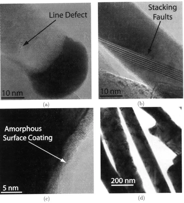
1-5 High-resolution TEM micrographs showing (a) lattice imaging and a
line defect in a single crystal silicon nanowire (dark region is the growth catalyst), (b) stacking fault defects in a single crystal silicon nanowire, (c) an amorphous coating residing at the edge of a nanowire, and (d) polycrystalline nickel nanowires. Images courtesy of J. Huang, Sandia National Laboratories. . . . . 20
1-6 An illustration of the kinetic theory model of energy transport in a gas. Heat diffuses from the hotter wall (T) to the colder wall (T2) through molecular collisions whereby energy is transferred from gas particles
with higher energy to gas particles with a relatively lower energy. . . 22
1-7 A schematic illustration of the temperature-dependent thermal
con-ductivity of a bulk, non-metallic solid. . . . . 25 1-8 Bulk silicon thermal conductivity data as a function of temperature [20].
Approximate regions of the dominant phonon scattering mechanisms have been labeled. . . . . 27 1-9 Two microfabrication-based structures employed for measuring the
thermal properties of NTs and NWs. The structure shown in (a) is formed from two islands joined by either a NW or NT, with one is-land functioning as the heat source and the adjacent isis-land sensing a temperature rise due to heat flow [8]. The structure shown in (b) uses a single suspended heater line in contact with a CNT [25]. For a given power input, the temperature rise of the heater is measured with, and without, the NT present, and then the thermal conductance of the nanotube (or nanowire) is obtained. For the nanowires and nan-otubes measured with these devices, the thermal contact conductance was assumed to be a minor contribution to the total measured thermal conductance. ... ... 29 1-10 Thermal conductivity data for Si and Si-SiGe nanowires [4, 26]. The
1-11 Microfabricated devices for a comparative study of thermal
conduc-tance in nanowires [28]. The nanowires are the supports for the central structure and possess beam geometries of 6 pm, 250 nm, and 150 nm for the length, width, and thickness, respectively. . . . . 31
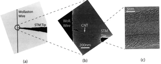
1-12 (a) The TEM compatible hot wire probe consisting of an etched Wol-laston wire stretched and epoxied across a quartz support frame. The entire structure resides on the end of a custom TEM holder with an STM tip manipulator. (b) An etched Wallaston wire with the Pt core exposed. ... ... 32 1-13 A series of micrographs showing the Wollaston wire probe, the STM
tip, and the CNT that was measured at various magnifications. The Wollaston wire probe mounted in the TEM at a lower magnification is shown in (a). At an increased magnification, (b), the CNT can be seen physically connecting the Wollaston wire and the STM tip. At a magnification nearly reaching the limit of the TEM, the individual walls of the CNT can be seen, (c). . . . . 33
2-1 Qualitative spatial temperature distributions for a suspended heater (a) and the same heater in contact with a nanowire (b). The presence of the nanowire (shown in green) reduces the overall temperature of the heater but functioning as a heat sink to thermal ground. . . . . . 38
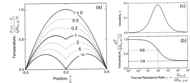
2-2 The coordinate system used for modeling heat transfer in the heater/thermometer and the nanowire. . . . . 39 2-3 Graphical solutions to the heat equation for a suspended, Joule-heated
structure with a nanowire in thermal contact at the structure's mid-point. (a) Temperature distributions for various values of thermal resistance ratios. (b) The normalized mean temperature rise of the suspended heater for various values of -y. (c) Dimensionless sensitivity,
s, (see text) as a function of -y. The maximum sensitivity occurs when
2-4 Temperature-dependent thermal conductivity of bulk Pt [37]. The in-set shows only a fraction of the full temperature range, emphasizing that the thermal conductivity of bulk Pt changes by less than a factor of 2 over a wide range of practical temperatures. . . . . 48
2-5 (a) A microfabricated platinum wire used in a 4-point I-V measurement to determine the electrical properties of an electron-beam evaporated platinum thin film. (b) Electrical resistivity as a function of tempera-ture for the fabricated thin film structempera-ture. Bulk Pt electrical resistivity is shown for comparison [37]. . . . . 49
2-6 A thermal circuit for modeling the Pt/SiNx composite beam as two,
parallel thermal resistors . . . . 50
3-1 An optical image of the microfabricated chip placed near a dime for
scale (a). An optical image of the gold electrodes and contact pads is given in (b), and a micrograph showing the Pt suspended heater line at the very center of the device (c). . . . . 54
3-2 The Si wafer after oxidation and nitride deposition. The thin gate
oxide aids in mitigating pin-hole defects in the much thicker nitride lay er. . . . . 56 3-3 A schematic illustration of the initial window size (x) and the
result-ing membrane width (w). The hypotenuse of the h-s right triangle represents the <111> plane, where h is the thickness of the wafer and 6 = 54.7 . . . . . 57
3-4 (a) The Si wafer with both dielectric films and photoresist on the sur-face selected for pattern transfer. (b) The developed pattern of a sin-gle etch window after exposure using contact lithography (Hundreds of these patterns exist on a single wafer). (c) A single etch window with the oxide and nitride layers removed after dry etching. . . . . 58 3-5 Si TMAH (25%) etching rate normal to the {100} plane as a function
3-6 The TMAH etch bath consisting of a Wollam condenser and a
temperature-controlled hotplate (a). Cooling water is provided by a recirculating constant-temperature bath shown in (b). . . . . 60
3-7 A photograph of a wafer after the TMAH wet-etching process. The
observed color gradient is due to a slight thickness variation in the SiNX thin film . . . . 61
3-8 (a) The top surface of the device showing the released SiNX membrane,
and a micrograph of the etch via (b), showing the
{
1111 planes and a minor undercut in the Si on the back-side of the device. The two images have been rotated 90' with respect to each other. . . . . 623-9 A illustration of the device after completion of the TMAH Si wet-etch
process. Due to the higher etching rate of SiO2 compared to that of SiNX in TMAH, the SiO2 layer will experience a slight undercut. . . . 63
3-10 (a) An SEM micrograph showing the EBL alignment marks used for
aligning the desired electrode pattern to the SiNx membrane. . . . . . 65
3-11 The Si wafer with EBL resist (shown in orange)(a), the developed
pattern of the EBL resist, after exposure (b), Ti/Pt non-conformally coats the surface of the chip after e-beam metal evaporation (c), and the device with EBL-defined electrodes post lift-off (d). . . . . 65
3-12 A micrograph showing the top surface of the device after the EBL
metallization step. The metal contamination areas around the formerly clean alignment marks are from electron beam exposure during the pattern alignment process. . . . . 66
3-13 The chip with photoresist (a), After exposure and resist development,
voids remain where metal ultimately will be deposited (b), The e-beam evaporated Ti/Au layer, covering both the resist and the previously exposed SiNx regions (c), The fully metallized device after the lift-off procedure. Although not seen from this perspective of the illustration, the Ti/Au layer makes physical contact to certain locations of the Ti/Pt electrodes where intended (d). Note that the illustration is not to scale and that the metal electrodes on the surface, present during
the resist spin, are approximately 1/14 of the height of the resist. . . 67 3-14 An SEM image showing the device after the large-area leads were
pat-terned. The overlap between the Ti/Pt layer and the Ti/Au layer is recognizable from the bright edge produced by secondary electrons in the SE M . . . . . 68 3-15 PMMA is spun on to the top surface of the chip (a). After EBL and
development, selected areas of SiNx are exposed (b). After the CF4
dry etch, the previously exposed areas of SiNx are eliminated (c), and after the resist is stripped, only the Pt/SiNx composite beam structure remains at the center of the opening. . . . . 69 3-16 A micrograph showing the EBL region of the device after the dry-etch
step. Note that the areas exposed during alignment were etched as well. 70
3-17 A collection of GaN nanowires on their growth substrate (a). After
the transfer process, nanowires that were originally on the growth sub-strate are now suspended in various locations on the TEM grid. One particular location on a TEM grid is shown in (b), where the nanowire is both well isolated and readily accessible to attachment by either a sub-micron or micron-sized probe. . . . . 71 3-18 An SEM micrograph showing the nanowire placement procedure. Shown
in the image are the two iridium probe tips and a GaN nanowire being placed near the center and perpendicular to the suspended heater line. 72
3-19 The placed nanowire and EBID Pt top contacts. Temperature
depen-dent thermal conductivity measurements on this device are presented in C hapter 5. . . . . 73
4-1 A single lock-in amplifier and ballast resistor arrangement for measur-ing the intrinsic resistance of an electrical resistor. In this arrangement, a separate voltage source may be implemented and referenced to the lock-in amplifier, or the oscillator from the lock-in amplifier may be used as the voltage source. . . . . 79
4-2 Oscillator stability measurement for 1 hour scan. Results are similar with and without a resistive load on the oscillator output. All data was offset such that the intitial data point in each data set was 100 mV. In this test two Signal Recovery 5210 LIAs and two SR830 LIAs were examined, with only one Signal Recovery 7265 LIA tested. . . . . 80
4-3 7265 oscillator voltage amplitude scans for 10 mV, 100 mV, and 1 V, monitored over a time duration of approximately 20 minutes. Oscilla-tor stability improved with increasing oscillaOscilla-tor amplitude. . . . . 82
4-4 Temperature fluctuation of the ambient laboratory environment over a 24-hour period. The blue highlighted region encapsulates an approx-imate 1 K/hr. temperature decline. The data was acquired with an Oakton brand temperature logger. . . . . 83
4-5 Dual lock-in amplifiers in a half-bridge arrangement measuring the voltage across a precision, low-TCR, current-sense resistor and the voltage drop across an unknown resistor. . . . . 85
4-6 Voltage measurements of a 100 Q resistor for a time duration of ap-proximately 15 minutes. The ordinate is the percent deviation of the voltage measured from the mean voltage of the entire data set sampled. 89
4-7 The experimental apparatus with major components labeled. All equip-ment, excluding the He compressor, was arranged on an optical table, with the cryostat, vacuum pump, and data acquisition computer sit-ting directly on the table and breakout panel, lock-in amplifiers, and temperature controller stationed on a shelf above the table. . . . . 92
4-8 The three HP 34904A 4x8 switch array boards. The upper board per-forms the task routing source inputs and sense signals, while the bot-tom two boards control signal flow to connections 1-16. Blue labels indicate external connections for inputs and outputs, and gray H and L labels indicate unused terminals. . . . . 96
4-9 A photograph of the assembled switch array boards, before installation into the HP 34970A chassis. The ballast resistor bank inside of board 1 can be identified from the white and yellow colored shrink wrap. . . 97 4-10 A schematic illustration showing the major electronic components
in-corporated into the measurement system and their signal paths to the measurement device, which is mounted inside of a cryostat. Lock-in amplifiers (pair 1) source and sense lines are routed via the switch array to the breakout panel, where as the source and sense lines from lock-in
amplifiers (pair 2) connect to the breakout panel directly. Note: All source and sense leads shown indicate a high/low pair. . . . . 99
4-11 The packaged device mounted onto the cryostat's sample holder. The microfabricated device is shown at the center of the 24-pin dual inline package (DIP) header, which is mounted to the 24-pin socket. The thin-film heater is shown encapsulated in black Stycast epoxy. Also shown are the two Si diode thermistors used by the temperature con-troller for monitoring and controlling the temperature of the sample holder. The temperature difference between Si diodes A and B was typically on the order of 100mK in the temperature range of 20-300K. 100 4-12 The packaged device mounted onto the sample holder and thermally
4-13 An illustration showing the center region of the ideal device. The gray areas represent the Pt metallized regions, the black area is where the SiN, was removed by etching, and the purple area represents the SiNX surface. Also shown are the Pt heater electrical leads that would source and drain the current, I, and the voltage sense leads, V1 and V2. . . 102
4-14 A micrograph of the fabricated T-structure. The ligament, spanning from the center of the Pt heater line to edge of the opening, emulates the presence of a nanostructure. . . . . 104
4-15 Heating curves for the T-structure at 295 K. With the thermal link (ligament) present, the mean temperature rise above the ambient is lower for a given input power, compared to when the thermal link has been rem oved. . . . . - - . 106
4-16 A micrograph of the T-structure with the ligament severed. The inset shows the ion-beam cut of the thermal link at greater magnification. . 107
5-1 The growth and geometry of GaN nanowires. (a) A section of cleaved growth substrate showing the vertical orientation of the GaN wires to the sapphire growth substrate. (b) A direct view of a GaN nanowire's triangular cross-section, which is essentially equilateral. The tapered nature of the wire along the growth direction is shown in (c). Typical values for the amount of taper observed in the GaN nanowires were 6w/L - 10 nm/pm, where w and L are the width and length of the
nanowire, respectively. . . . .. . . .. . . . .. 114
5-2 A single nanowire treated as two, separate wires, labeled as sections "1" and "2". The rectangular regions on the wire represent the Pt top
contacts. . . . . 115
5-4 A microfabricated measurement platform with a nanowire placed on the suspended heater/thermometer. A micrograph taken at a relatively low magnification is given in (a), which shows the nanowire placed perpendicular to the suspended heater. Also shown are the heater's current and voltage leads, and an auxiliary thermometer. (b) A higher magnification image showing the nanowire immediately after its place-ment onto the heater. (c) The GaN nanowire after the patterning of electron beam induced deposition (EBID) Pt contacts. . . . . 119 5-5 Resistance thermometry data for the suspended heater/thermometer.
(a) The cold-wire electrical resistance, R,, as a function of ambient temperature, T,. (b) The temperature coefficient of resistance (TCR), a, based on the values of R, shown in (a). For comparison, bulk Pt TCR values have been plotted as well. [37] . . . 120
5-6 Heating curves and GaN nanowire cutting. (a) The combined heating
curves generated at 295K. As each GaN nanowire is cut, a thermal path to ground is removed and for a given input power, the heater's average temperature increases. (b) Transmission electron micrographs showing one of the GaN nanowires after the wire-cutting process. In this micrograph, the dark line at the top of the image is the suspended heater/thermometer and the dark line at the bottom of the image is the Pt contact at the lower boundary. . . . . 121
5-7 Transmission electron microscopy of the 215 nm wide (based on an
av-erage width) GaN nanowire on the microfabricated device. (a) A TEM image of the placed GaN nanowire at a modest magnification showing a mild amount of strain in the wire. (b) A high-magnification image of one edge of the nanowire. The small crystalline clusters on the surface of the wire are the result of contamination from the EBID carbona-ceous Pt contacts. The inset shown in (c) is a select-area diffraction image and reveals the single crystal nature of the nanowire. . . . 122
5-8 Temperature dependent thermal conductance data for the 215 nm and 295nm GaN nanowires. . . . . 123 5-9 Temperature dependent thermal conductivity data for GaN nanowires.
The data for the 215 nm and 295 nm nanowires are results from this thesis work. The data for the 160 nm and 181 nm nanowires was ob-tained by Guthy et al. [50]. . . . . 125 5-10 A thermal resistance network consisting of the thermal resistance due
to a single nanowire, a spreading resistance, and two, series thermal contact resistances. . . . . 126
Chapter 1
Introduction
Over the last several years, nanowires have attracted considerable attention. Semi-conductor nanowires can be synthesized into both axial and radial heterostructures, with typical diameters ranging from 10 -100 nm and possessing lengths on the order of microns [1, 2]. Theoretical work on the electronic properties of nanowire systems predict that these materials should behave much differently than their bulk counter-parts [3], and previous experimental work on the thermal properties of nanowires has demonstrated that classical size effects are present in these systems [4]. These unique attributes of nanowires, coupled with their large surface-to-volume ratio, could po-tentially provide a technological path forward for various new types of biosensors [5], optoelectronics [6], and thermoelectrics [7]. With respect to fundamental studies on nanowires, considerable work has been conducted on characterizing the electrical properties of nanowires, with the thermal properties of nanowires being less under-stood. The defects within a nanowire and the surface morphology of a nanowire could potentially impact its transport more significantly than if it were in bulk form; however, to date, only a limited amount of information exists in which the atomic structure of a nanowire has been correlated to its measured transport properties [8]. One reason for this paucity of structure-transport information is that the transport measurements on single nanowires are challenging, and obtaining atomic structure information on exactly the same wire measured introduces an immense level of com-plexity to the measurement.
The work presented in this thesis addresses the issue of relating a nanowire's atomic structure to its measured thermal transport properties by developing a mi-crofabricated measurement platform that is compatible with a transmission electron microscope.
The material in this chapter presents an introduction to nanowires, which briefly describes nanowire synthesis and presents examples of proof-of-principle nanowire de-vices. An introduction to transmission electron microscopy is presented, which, using results from prior microscopy studies on various nanowires, emphasizes the neces-sity for correlating the atomic structure of nanowires to their transport properties. With a focus on thermal transport, the physical origins of the thermal conductivity in bulk solids is discussed. Prior work using microfabricated devices for measuring the thermal properties of individual nanowires and nanotubes is presented. The thermal conductivity data obtained on nanowires using these microfabricated structures shows that the thermal conductivity of ~ 100 nm diameter nanowires is reduced consider-ably compared to their bulk counterpart. An approach for measuring the thermal conductivity of an individual nanowire or nanotube that does not required micro-fabrication but does allow transmission electron microscopy capabilities is presented. The material in this chapter also highlights how one may leverage the reduction in a nanowire's thermal conductivity as a means of improving thermoelectric device efficiencies.
1.1
An Introduction to Nanowires
The chemical vapor deposition (CVD) synthesis of semiconductor nanowires, apart from the mechanism of determining the wire's diameter, utilizes the same established synthesis methods as those used in the synthesis of CVD thin films. The following sections briefly describe the CVD process for nanowire synthesis, show examples of axial and radial nanowire heterostructures, and present a few proof-of-concept nanowire devices.
1.1.1
Nanowire Synthesis
In 1964, while working at Bell Telephone Laboratories, researchers Wagner and Ellis discovered a technique for synthesizing nanowires, and they referred to the technique as vapor-liquid-solid (VLS) growth [9]. At the time (circa 1960), Wagner and Ellis referred to the synthesized silicon wires as "whiskers". Over 30 years later, this method of synthesizing a nanoscale wire was rediscovered [10, 11].
In the VLS process a growth substrate typically is placed in a CVD furnace. Taking as an example the growth of a silicon wire, the CVD furnace is filled with silane gas. The substrate, which for example could be Si, is coated with a thin film ~1 nm
-10 nm of metallic growth catalyst (typically Au) on its surface. Once the CVD furnace
is heated, the Au film melts at the Au/Si eutectic temperature, and the Au coalesces, essentially covering the Si substrate with nanometer-sized droplets of Au. When the silane decomposes in the CVD furnace, Si, in the presence of the Au droplets, forms a Au/Si alloy. Once the level of Si supersaturates in the Au/Si droplet (which can be determined from a Au/Si binary phase diagram), Si in solidus form precipitates from the droplet forming a nanowire. As more Si diffuses from the gas phase (vapor) into the Au/Si alloy (liquid), it grows epitaxially at the liquid/solid interface producing the wire (solid). Figure 1-1 shows an illustration of the process. The VLS growth process can be used to synthesize single-crystal nanowires and dopant gases such as arsine, phosphine, and/or diborane may be introduced into the source gas stream to dope the wire.
Semiconductor nanowires can be grown into both axial and radial heterostruc-tures [1, 2]. A common (but not trivial) method for growing heterostructured nanowires consists of alternating the nanowire source gas to produce an axially segmented nanowire that consists of the various sources [1]. Heterostructured NWs also may be formed radially. By alternating reactant gases after the core NW has been grown, one may form thins shells of various other desired materials around the NW core, forming a core-shell nanowire. Transmission electron micrographs of both axial and
Solid Precipitate (Nanowire)
Soi
\/,-Figure 1-1: The vapor-liquid-solid growth process. The catalyst droplet in liquid form reacts with the source vapor to form an alloy. Once the alloy droplet reaches a, critical concentration of the source material, the source precipitates from the liquid alloy, forming the nanowire.
(a) (b)
Figure 1-2: Transmission electron micrographs showing (a) axial nanowire het-erostructures consisting of Si/SiGe [1], and (b) an i-Si/SiOx/p-Si nanowire [2]. The oxide layer (< 1 nm) cannot be observed in this image, but the interface (dashed line)
between the crystalline core and amorphous coating exhibits a structural difference and illustrates the disruption of epitaxy in radial growth. Inset, TEM image of p-Si coating the nanowire and the Au nanocluster tip. Scale bar is 50 nm.
1.1.2
Proof-of-principle Nanowire Devices
The demonstration of single- and multiple-nanowire devices has been realized over many disciplines of science and engineering. This section highlights only a small fraction of such devices.
As a bottom-up design approach to nanoelectronics, core-shell NW structures were formed into FETs [2]. Figure 1-3 (top-left) shows a micrograph of the fabricated device, with the source, gate, and drain electrodes labeled, and representative data.
Nanowire arrays have also been used to sense biomolecules [5]. In this work (Fig. 1-3 top-right), the surface of the nanowire is functionalized and the electrical conduc-tance of the nanowire measured. When a biomolecule is introduced into the solution surrounding the nanowire, it binds to the surface and the electrical conductance of the wire is altered; an effect which exploits with high surface-to-volume ratio of a nanowire. Researchers also have fabricated and patterned arrays of ZnO nanowires, which, when optically pumped, produce coherent light in the UV range [6]. In their findings, the well-faceted nanowires behaved as natural resonance cavities. An image of the epitaxially grown ZnO nanowires and emission data is given in Fig. 1-3 (bottom-left). As a last example, researchers were able to utilize the mechanical properties of a single nanowire to develop a mechanical resonator [12]. As shown in Fig.
1-3 (bottom-right), the mechanical resonator is formed by a suspended nanowire, which
is clamped at both ends. For this device, the natural resonance frequency at cryogenic temperatures was approximately 100 MHz.
1.2
An Introduction to Transmission Electron
Mi-croscopy
Transmission electron microscopy is perhaps one of the best microscopy tools for gaining an understanding of the atomic structure of a material. Scanning tunneling microscopy (STM) provides information regarding the electronic density of states at the surface of a material. Although STM can provide atomic resolution of a
mate-Figure 1-3: Demonstrated nanowire devices: A field-effect transistor developed using a radial nanowire heterostructure [21; a biological sensor demonstrating the ability to functionalize the nanowire's surface and sense biomolecules by altering the electrical conductance channel in the nanowire [5]; optically pumped lasing from a forest of nanowires [6]; and a mechanical resonator formed from a single nanowire [12].
rial, the specimen under examination must be electrically conductive and possess a pristine surface, which in practice requires that the sample be heated to a relatively high temperature to liberate impurities from the material's surface. Atomic force mi-croscopy (AFM), which can be performed in both atmospheric and ultra-high vacuum conditions, can provide detailed information about the surface morphology of a mate-rial. However, acquiring atomic resolution of a material's surface with an AFM is not a trivial procedure. A high-resolution scanning electron microscope (SEM) permits a ~1nm probe beam, but an SEM will only provide information about the morphology of a surface. Transmission electron microscopy can provide sub-Angstrom resolution; however, the material must be electron transparent (typically < 500 nm) and in some instances, the process of imaging the sample could result in irreversible sample dam-age. The following sections provide an introduction to TEM and present material on the benefits of TEM on individual nanowires.
1.2.1
Interactions with Electrons and Matter
In general, radiation can be defined as energy transport in the form of waves or trav-eling subatomic particles and may be either ionizing (capable of removing tightly bound inner-shell electrons from matter) or non-ionizing. Highly energetic electrons produced by the TEM are a form of ionizing radiation. Upon incidence with the speci-men under inspection, these electrons may be transmitted directly through the sample or scattered elastically or inelastically. Incident electrons may also be backscattered
(i.e., reflected) by the specimen or absorbed by the material and thus generate heat or form electron-hole pairs. The ionizing effects of the incident beam create a variety of secondary signals, as shown in Fig. 1-4. These secondary signals allow one to per-form chemical (or elemental, rather) analysis on a specimen, by employing techniques such as X-ray energy dispersive spectrometry (XEDS) and electron energy loss spec-trometry (EELS), which provide information about the chemical composition of the specimen.
Incident e- Beam
Backscattered e- Secondary
e-Visible Light Characteristic
r-y X-rays Excitons Absorbed e Spedmen Elastically Inelastically Scattered e-Scattered e~ Direct e- Transmission
Figure 1-4: A TEM specimen and the secondary signals generated when a highly energetic beam of electrons is incident upon the specimen. Secondary signals emitted from the specimen can provide valuable information regarding the elemental compo-sition of the sample.
1.2.2
Transmission Electron Microscopy of Nanowires
As previously mentioned, transport measurements on nanowires typically are not ac-companied by transmission electron microscopy on the wire measured. In the few cases where TEM is performed, it is done typically on a representative sample that is not the same sample on which transport measurements were performed. Because of the high surface-to-volume ratio in nanowires, the morphology of the nanowire's sur-face becomes extremely important. Information regarding the roughness of the wire's surface and how the wire's surface terminates are important pieces of information if one is to understand the role of surface scattering on the wire's transport behavior. Knowledge of the atomic structure internal to the wire is equally important. If the nanowire is polycrystalline, rather than single crystalline, grain boundaries will affect transport. If the nanowire possesses numerous defects, such as stacking faults, these disruptions in the crystal will likely impede transport. Knowledge of the crystal-lographic growth direction is important also, as many materials possess anisotropic transport properties.
Figure 1-5 shows TEM micrographs of various nanowires. The high-resolution TEM images shown in Fig. 1-5 (a) and (b) highlight line and stacking-fault defects,
which can be present in a nanowire. The presence of stacking faults in the nanowire are possibly more critical towards impeding transport than line defects. An amor-phous coating present on the surface of the nanowire is shown in Fig. 1-5 (c). Imaging this structure in the TEM provides a more accurate representation of the nanowire's cross-sectional composition, compared to simply relying on an SEM image where one may be inclined to believe that the entire conduction cross-section is the entire diameter observed, when in reality only a portion of the observed cross-section is con-tributing to transport. Figure 1-5 (d) reveals the polycrystalline nature of a particular Ni nanowire sample. For a single nanowire that has been characterized electrically and/or thermally, transmission electron microscopy performed on exactly the same wire can provide structural information about the nanowire and allow one to better understand the measured transport data.
1.3
Heat Conduction and Thermal Conductivity
Heat transfer in a solid can occur through various mechanisms. In semiconductors and dielectrics, heat conduction transpires through thermal vibrations of the atoms in the solid. In metals, thermal vibrations play only a minor role in heat conduction, as the majority of heat is conducted by free electrons in the metal. The following sections focus on the physical nature of heat conduction in bulk semiconductors and the mechanistic length scales associated with heat carriers due to classical size effects.
1.3.1
Physical Origins of Thermal Conductivity in Bulk
Ma-terials
In 1822 Jean Baptiste Joseph Fourier published his treatise on the theory of heat conduction [13]. Fourier stated that the heat flux (or the heat transfer rate per unit area) q" resulting from thermal conduction was proportional to the temperature gradient, VT , and opposite to it in sign. The constant of proportionality, k, is referred to as the thermal conductivity, and is a temperature-dependent material
(b)
w
(c) (d)
Figure 1-5: High-resolution TEM micrographs showing (a) lattice imaging and a line defect in a single crystal silicon nanowire (dark region is the growth catalyst), (b) stacking fault defects in a single crystal silicon nanowire, (c) an amorphous coating residing at the edge of a nanowire, and (d) polycrystalline nickel nanowires. Images courtesy of J. Huang, Sandia National Laboratories.
property. Phenomenologically, Fourier's law states that heat flows from a region of higher temperature to a region of lower temperature, and mathematically, it takes the following form
q" =-kVT. (1.1)
Heat conduction in a solid, in the most fundamental sense, is a direct result of microscopic activity in a material due to the absence of thermodynamic equilibrium. In metals, the primary carriers of heat are electrons [14]. In both nondegenerately doped semiconductors and dielectrics, lattice (atomic) vibrations are the dominant heat carrier [14, 15]. Lattice vibrations in a region of a solid are directly proportional to the corresponding local temperature. Because the atoms in a solid are closely coupled, a region of higher vibration (i.e., higher temperature) will transmit energy to regions of lesser vibration (i.e., lower temperature). Thus, in non-metallic solids, the heat conduction process can be viewed as the transfer of energy from highly energetic
atoms, to atoms of lower energy, through atomic interactions. The numerous atomic vibrations occurring in a crystalline solid can be decomposed into normal modes of
vibration, and quantized normal modes of vibration are called phonons.
The physical nature of heat conduction can be understood by constructing an analogy between gas molecules in a container and atomic vibrations in a solid. Fig-ure 1-6 is an illustration of a gas confined to a container in which a temperatFig-ure gradient exists. In this system, two surfaces are maintained at different teimpera-tures, T1 and T2, where Ti > T2. The temperature at a particular location in the gas is associated with the energy of a gas particle at that location. For non-monatomic gases, the energy of a gas molecule would not only consist of the molecule's transla-tional energy, and therefore the energy would consist of an amalgam of vibratransla-tional, rotation, nuclear, and electronic energies. In the gaseous system (Fig. 1-6) gas parti-cles at higher temperatures exist at higher energetic states, relative to gas partiparti-cles at lower temperatures. When gas particles undergoing random motion collide, a more energetic particle will transfer energy to a less energetic particle. The diffusion of heat
from the hotter wall to the colder wall is the net transfer of energy due to particle collisions.
////7////////////
2
T > T
12
XI
I
I
X- VT XO XO+ V T 0- XT X+ TX0X
XX xoFigure 1-6: An illustration of the kinetic theory model of energy transport in a gas. Heat diffuses from the hotter wall (T1) to the colder wall (T2) through molecular collisions whereby energy is transferred from gas particles with higher energy to gas particles with a relatively lower energy.
Aside from a physical picture of heat conduction, the kinetic theory model can also provide insight into the physical nature of thermal conductivity. Following a similar one-dimensional analysis as described in [14, 16, 17, 18], the net heat flux across a plane at x = x, which is perpendicular to the heat flow in the x-direction, is the difference in heat fluxes from the positive and negative x-directions. In a similar sense that the electrical current density (or current flux) in a conductor is proportional to the product of charge and carrier velocity, the heat flux is proportional to the product of energy and velocity. Assuming that heat carriers move with an average random velocity v and can travel a distance of Vgr before a collision with a neighboring heat
carrier occurs and alters their trajectory, the net heat flux in the positive x-direction at location x, can be written as
1
q net = q" (xO - VeT) - q"(xo +VsT) =jVX [U(xo - VXrT) - U(xo + vxT)] (1.2)
where v is the x component of velocity (assumed to be an average value), T is the average time between collisions, and U is the local energy density. For a stationary medium in which no bulk motion of the gas occurs, approximately one-half of the total number of carriers will travel in the positive x-direction and the remaining half will travel in the negative x-direction, which gives rise to the 1/2 pre-factor. Assuming
v2 = v2/3 and recognizing that a system with a constant transport cross-section, in
the absence of any internal heat generation, has a constant heat flux, then qx>,net = qx.
Using a first-order Taylor series expansion, the heat flux may be written as
/I d(Uvx) V2 dU dT
q = -VxT (1.3)
dx 3 dT dx
Noting that the quantity dU/dT is the volumetric specific heat, C, and writing the carrier mean free path (the average distance a heat carrier travels before a scattering event) as A = VT, the following expression for the heat flux is obtained
1 dT dT
qx= -
3
--Ce Adx
= -k (1.4)dx
which is Fourier's law for heat conduction in one dimension. From this kinetic-theory based model, the thermal conductivity may be expressed as
1
k = --CvA. (1.5)
3
Equation 1.5 shows that the thermal conductivity is a product of the carrier specific heat, velocity, and mean free path. The kinetic theory model for thermal conductivity is often used to estimate the mean free path of energy carriers, relying on experimental data for the thermal conductivity, specific heat, and average velocity (i.e., the sound
velocity of a solid).
An important difference between molecular and phononic systems and the de-termination of the carrier mean free path is that gas molecules may be described adequately by Maxwell-Boltzmann statistics, with the molecules' number density, energy, and momentum being conserved, but phonons obey Bose-Einstein statistics and therefore do not conserve number density nor (in all cases) momentum, but do follow energy conservation. Thus, whereas a hard-shell sphere model may be used to determine the mean free path of a system of molecules [18], the task of calculating the mean free path 1 for a system of phonons is often more challenging.
1.3.2
Mechanistic Lengthscales
The kinetic theory model of thermal conductivity, although simple, is a useful tool for gaining insight to the temperature dependence of the thermal conductivity of a solid. Focusing on heat conduction in non-metals due to phonon transport, Eqn. 1.5 states that the thermal conductivity is proportional to the phonon specific heat, C = Cph
, the average phonon velocity (speed of sound in the material), V =Vph , and the phonon mean free path, A = Aph. Considering the average phonon velocity in the material to be independent of temperature [19], the temperature behavior of the thermal conductivity may be deduced from the temperature-dependent nature of the phonon specific heat and mean free path.
At low temperatures, interactions among phonons decreases and Aph tends to-ward a constant value that is representative of the size and shape of the sample. In this low-temperature regime, phonon-phonon scattering is decimated because of the minimal atomic nucleus displacements and lattice vibrations approximating simple harmonic motion, which prohibits phonon interactions. In this regime, Aph is said to be dominated by boundary scattering. At intermediate temperatures, e.g., 1 K-100 K,
Aph is limited by impurity scattering in the material. At temperatures comparable
'The phonon mean free path for a system is mode (frequency) dependent, i.e., Aph = Ap, (W),
and thus, a single Aph value cannot completely describe the behavior of a system of phonons in their entirety. When a single value of Aph is reported or estimated, it is often assumed that this value represents an average value.
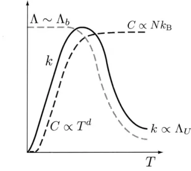
to or above the Debye temperature (OD), e.g., OD = 645 K in Si, Aph is limited by 3-phonon (Umklapp) interactions and is inversely proportional to temperature. A qualitative plot of Aph transitioning between the limits of boundary (Aph ~ Ab) and Umklapp (Aph ~ Au) limitations is shown in Figure 1-7.
A-Ab
C _o NkB
k
|
/C oc Td
k oc
AU
T
Figure 1-7: A schematic illustration of the temperature-dependent thermal conduc-tivity of a bulk, non-metallic solid.
For multiple, independent scattering mechanisms, the effective phonon mean free path is given by Matthiessen's rule 2
1 - _= _1 -- 1 1
+ + (1.6)
Aph Ab Aim Au
here, Ab, Aim, and AU are the phonon mean free paths limited by boundary, impurity,
and Umklapp scattering processes, respectively.
The specific heat of a solid at high temperatures is approximately a constant value and approaches the limit of Dulong-Petit, where all phonon modes are active. As the temperature decreases, the number of available phonon modes decreases and
2In this formulation, the effective carrier concentration is assumed below a degenerately doped
the specific heat functionally exhibits a Td relationship, where d represents the di-mensionality of the system (e.g., d = 3 for a bulk, 3-D structure and d = 1 for quasi 1-D structures).
Figure 1-7 illustrates that the lattice thermal conductivity, k, of a solid is reduced at low temperature due to a reduction in the phonon contribution to the specific heat. At moderate temperatures the lattice conductivity achieves a peak value, with the peak height being inversely proportional to the impurity concentration in the solid. In the high-temperature regime, the lattice conductivity is proportional to a 1/T temperature dependence, and thus it asymptotically approaches a minimum value for increasing temperature due to non-momentum conserving phonon scattering processes.
Figure 1-8 shows temperature-dependent thermal conductivity data for bulk sil-icon, with sketches of T3 and T-1 slopes overlaid onto the data in the low and high-temperature regions. In the low-temperature region where phonon boundary scattering dominates, the thermal conductivity decreases due to a decreasing phonon population and nearly approximates the k oc T3 dependence. In the high-temperature
region where phonon-phonon scattering dominates, the bulk Si data exhibits a crude
k c< T-1 behavior.
Because nanowires possess diameters typically in the range of 10 - 100 nm, the thermal conductivity of a nanowire is expected to be lower than that of its bulk counterpart. This expected reduction in the thermal conductivity for a micro- or nanoscale structure is called a classical size effect and is a direct result of the phonon mean free being limited by the boundary of the structure, i.e., Aph ~ Ab. From Eqns. 1.5 and 1.6 one will note that when Aph~ Ab~ dNW, where d is the diameter of the nanowire, the thermal conductivity of the nanowire scales with its diameter,
k ~ dNW. However, in solids, a broad range of mean free paths is responsible for heat
conduction [21, 22], and thus, size effects in nanowires can appear at length scales greater than that predicted by Eqn. 1.5.
10000 3 4e T 1000 -~0 0 ) 1 0 100 boundary E impurity phonon - phonon 10 , '-o 1 f 10 100 1000 Temperature, T (K)
Figure 1-8: Bulk silicon thermal conductivity data as a function of temperature [20]. Approximate regions of the dominant phonon scattering mechanisms have been la-beled.
1.4
Prior Work and Challenges in Measuring the
Thermal Conductivity of Individual Nanotubes
and Nanowires.
Several technical challenges must be addressed when measuring the thermal prop-erties of individual nanowires (or nanotubes). Nanowires typically are synthesized as either forests of wires on a substrate or in templates [23], and thus, obtaining a single nanowire of a desired size from the host material can be a formidable task. The relatively high thermal resistances of nanowires require that one provide ad-equate thermal isolation such that parasitic heat paths do not obscure the results from a thermal conductivity measurement. Furthermore, accurately determining the temperatures at the ends of a nanowire in a thermal conductivity measurement can become problematic if the thermal contact resistance is comparable to or greater
than the intrinsic thermal resistance of the nanowire. If methods such as resistive thermometry are employed to perform temperature measurements, good temperature stability is required and both accurate and precise electrical measurements must be performed. In the following section, examples of measurements on single nanowires and nanotubes where several of the aforementioned technical challenges have been addressed is given.
Over one decade ago, researchers successfully measured the thermal conductivity of carbon nanotube bundles [24], and recently, research groups have measured the thermal conductivity of individual nanowires and individual carbon nanotubes [4, 8, 25] using microfabricated structures. Microfabricated devices facilitate a natural transition between the geometry of a nanoscale specimen and macroscale laboratory equipment, allowing one to communicate with a nanoscale structure, electrically (e.g., microscale electrodes or probe tips), thermally (e.g., microfabricated heaters or laser heating with micron-sized beam spots), and optically (near-field scanning optical microscopy).
Two examples of single nanowire and nanotube measurements employing micro-fabrication are shown in Fig. 1-9. Both of the structures shown in this figure rely on placing a nanowire or nanotube (with either a liquid drop-casting technique or a mechanical manipulator) between structures that impose a temperature gradient on the sample with a prescribed amount of heat flow. The structures shown in Fig. 1-9 implement microfabricated resistive temperature devices (RTDs) to both function as heat sources and thermometers. With these devices, knowledge of the heat transfer rate,
Q,
and the temperature difference across the sample, AT is obtained, such that the thermal conductance, G = Q/AT, of the sample may be computed. The majority of the work reported on thermal transport measurements of both nanowires and nan-otubes rely on scanning electron microscopy to determine the geometry of the tube or wire, from which the thermal conductivity (k) can be determined, by k = GL/A,where L is the specimen's length and A is the transport cross-section. For trans-port measurements on nanowires or nanotubes, scanning electron microscopy only provides information regarding the surface morphology of the tube or wire and not
(a) (b)
Figure 1-9: Two microfabrication-based structures employed for measuring the ther-mal properties of NTs and NWs. The structure shown in (a) is formed from two islands joined by either a NW or NT, with one island functioning as the heat source and the adjacent island sensing a temperature rise due to heat flow [8]. The structure shown in (b) uses a single suspended heater line in contact with a CNT [25]. For a given power input, the temperature rise of the heater is measured with, and without, the NT present, and then the thermal conductance of the nanotube (or nanowire) is obtained. For the nanowires and nanotubes measured with these devices, the thermal contact conductance was assumed to be a minor contribution to the total measured thermal conductance.
information such as the defect density, number of tube walls, or perhaps the presence of an oxide coating on a nanowire.
Figure 1-10 shows thermal conductivity data for single crystalline Si nanowires and for Si-SiGe superlattice alloy nanowires measured using the device shown in Fig. 1-9 (a). Recalling that the thermal conductivity of bulk Si at 300K is kbuIk,si = 148 W/m-K, one will note that the thermal conductivity of the Si nanowires is ap-proximately a factor of 3 lower than for bulk Si, for the largest wire measured. For the superlattice Si-SiGe nanowires, the thermal conductivity reported for both wires is approximately a factor of 30 less than for bulk Si at 300K.
115nm 56nm 37nm AAAAAAAAAAAAAAAAAAAAAA * A A A 83nm 58nm 50 100 150 200 2 Temperature, T (K) 50 300 Single Crystal Silicon Si-SiGe Superlattice-Alloy 350
Figure 1-10: Thermal conductivity data for Si and Si-SiGe nanowires [4, 26]. The diameter of each nanowire measured is labeled in the plot.
This observed suppression in the thermal conductivity of Si and Si-SiGe nanowires could be used to enhance the performance of a thermoelectric device. The efficiency of a thermoelectric power generator is related directly to the thermoelectric device's dimensionless figure of merit, ZT, where
-
S2U_ZT = -T


![Figure 1-8: Bulk silicon thermal conductivity data as a function of temperature [20].](https://thumb-eu.123doks.com/thumbv2/123doknet/14732669.573386/39.918.223.699.120.508/figure-bulk-silicon-thermal-conductivity-data-function-temperature.webp)

![Figure 1-11: Microfabricated devices for a comparative study of thermal conductance in nanowires [28]](https://thumb-eu.123doks.com/thumbv2/123doknet/14732669.573386/43.918.149.774.589.834/figure-microfabricated-devices-comparative-study-thermal-conductance-nanowires.webp)