HAL Id: hal-01132832
https://hal.archives-ouvertes.fr/hal-01132832
Submitted on 18 Mar 2015
HAL is a multi-disciplinary open access
archive for the deposit and dissemination of
sci-entific research documents, whether they are
pub-lished or not. The documents may come from
teaching and research institutions in France or
abroad, or from public or private research centers.
L’archive ouverte pluridisciplinaire HAL, est
destinée au dépôt et à la diffusion de documents
scientifiques de niveau recherche, publiés ou non,
émanant des établissements d’enseignement et de
recherche français ou étrangers, des laboratoires
publics ou privés.
Monolithic integrated silicon-based slot-blocker for
packet-switched networks
Guilhem de Valicourt, Miquel A. Mestre, Laurent Bramerie, Jean-Claude
Simon, Eric Borgne, Laurent Vivien, Eric Cassan, Delphine Marris-Morini,
Jean-Marc Fédéli, Philippe Jennevé, et al.
To cite this version:
Guilhem de Valicourt, Miquel A. Mestre, Laurent Bramerie, Jean-Claude Simon, Eric Borgne, et
al.. Monolithic integrated silicon-based slot-blocker for packet-switched networks. 40th European
Conference on Optical Communication (ECOC 2014), Sep 2014, Cannes, France.
pp.We.3.5.5,
�10.1109/ECOC.2014.6963898�. �hal-01132832�
Monolithic Integrated Silicon-based Slot-Blocker
for Packet-Switched Networks
G. de Valicourt(1), M. A. Mestre(1), L. Bramerie(2), J.-C. Simon(2), E. Borgne(2), L. Vivien(3), E. Cassan(3), D. Marris-Morini(3), J.-M. Fédéli(4), P. Jennevé(1), H. Mardoyan(1),
Y. Pointurier(1), A. Le Liepvre(5), G. H. Duan(5), A. Shen(5) and S. Bigo(1) (1) Alcatel-Lucent Bell Labs, Nozay, France, [email protected]
(2) Université Européenne de Bretagne, CNRS, UMR 6082 Foton Laboratory, CS 80518, 22305
Lannion, France
(3) Institut d’Electronique Fondamentale (IEF), CNRS UMR 8622, Université Paris-Sud, Orsay, France. (4) CEA LETI, Minatec, 17 rue des Martyrs, F-38054 Grenoble cedex 9, France.
(5) III-V Lab, Joint lab of 'Alcatel-Lucent Bell Labs France', 'Thales Research and Technology' and
'CEA Leti', Campus Polytechnique, 1, Avenue A. Fresnel, 91767 Palaiseau cedex, France
Abstract We demonstrate a 16-channel, silicon-on-insulator, monolithic integrated slot-blocker. This
silicon photonic circuit includes two arrayed waveguide gratings, 16 variable optical attenuators and two vertical fiber couplers. We successfully operate it with 56 Gb/s and 80 Gb/s QPSK optical packets.
Introduction
Switching of optical data with sub-wavelength granularity (i.e. optical packets) enables statistical multiplexing, and thus increased network efficiency, while offering the possibility to remove opto-electronic conversions at intermediate nodes. In these nodes, optical packets simply flow transparently, unless they need to be dropped; which translates into energy savings. The transparent switching fabric is the part of the nodes where this process takes place, and therefore it is an essential part of the optical packet or slot switching paradigm.
Recently, this solution has been proposed for next-generation optical mobile backhaul
networks2 and datacenters3 where highly
dynamic adaptations to traffic variations as well as low-latency communication are needed. In optical slot switching (OSS) network, packets are sent into time-wavelength slots of the same
duration and a control channel carries the headers of each synchronous slot. Today the cost of the switching fabric, or slot-blocker (SB), including wavelength (de)multiplexer and optical gates, is still high and does not meet the cost requirements of the aforementioned network segments. Photonic integrated circuits are expected to provide large cost savings. Silicon photonics is a promising option to provide large-scale integration of photonic components with high-volume manufacturing compatibility. A few silicon photonic devices were proposed as optical gates, such as Mach Zehnder modulator (MZM)4, ring resonator5 and variable optical attenuator (VOA)6. Integration of silicon-based VOA combined with silica arrayed waveguide grating (AWG) in order to build a 1xN switching
fabric (with N+1 ports) was demonstrated6 but
lacked a second on-chip AWG to provide the slot blocking functionality within a 2-port package. In addition, silicon-on-insulator (SOI)-based integration of the AWGs and VOAs looks more promising to enable co-integration of the photonics and electronics in the same circuit. In this paper, we demonstrate a novel silicon photonic solution for OSS network. A 16-channels SOI-based monolithically integrated slot-blocker was designed, fabricated and tested. We demonstrate packet-switching operation for 56 Gb/s and 80 Gb/s quadrature phase-shift keying (QPSK) optical packets over all channels.
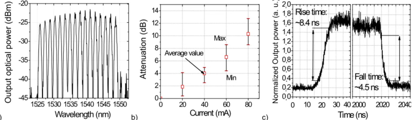
Devices fabrication and characterization Fig. 1(a) depicts the VOA-based node architecture where wavelength and packet selections are performed by the slot-blocker. To do so, a compact silicon circuit integrating two AWGs (200 GHz channel spacing), 16 high-speed VOAs and two vertical grating couplers
Fig. 1: slot-blocker circuit (a) schematic and (b)photography.
Vertical coupler grating Variable optical attenuator Array Waveguide Grating Electrical contact Passive silicon waveguide 4.1mm 1. 2 m m b) a) Add 2 1 2 1 3 . . . VOA VOA 2 1 . . . . . . 1 2 1 . . . . . . 2 1 Time Wavelengths Optical packets 3 2 Drop Emptied slot Transit
was designed and fabricated; see Fig. 1(b). The size of the full circuit was 4.1 mm × 1.2 mm. The chip was fabricated in 220nm overlayer SOI. First, grating couplers were patterned using
193 nm deep ultraviolet (DUV) lithography
followed by a 70 nm depth Si etching. Then the fabrication of the Si waveguides and the VOA parts were carried out with two self-aligned photolithography steps followed by two Si dry etching steps. The devices were then N and P doped on the 100 nm slab of the VOA part before cladding with 1 µm oxide. The electrodes were formed by DUV lithography and chlorine based reactive-ion etching. The calculated coupling efficiency of the grating couplers with a single mode fiber was around 4 dB. The excess losses of the grating couplers were mainly due to the fabrication imperfections (7 dB loss per vertical coupler, measured on a passive waveguide). The total insertion loss was around 22 dB which can easily be compensated with an Erbium Doped Fiber Amplifier (EDFA). The output spectra of all 16 channels are plotted in
Fig. 2(a). The wavelength channels were
designed with a 200 GHz spacing from 1525.9 to 1548.8 nm. The VOA was forward-biased in order to increase the propagation loss due to the
variation of carrier concentration. Fig. 2(b)
shows the attenuation as a function of the injected current for each channel; the average, maximum and minimum attenuations (across the set of gates) are represented for each value
of the injection current. An average static extinction ratio (ER) higher than 10 dB was measured for an 80 mA bias current. Then a 6V peak-to-peak squared electrical signal that switched every 2 µs between on and off states was applied (representing the erasure and non-erasure of 2 µs-long slots, respectively). The optical output power response under switching is shown in Fig. 2(c). For an average peak-to-peak voltage of 6 V, a dynamic ER of 9.7 dB was measured, with 10%-90% rise and fall times of 8.4 ns and 4.5 ns, respectively. Switching time of less than 10 ns is well below typical slot duration of a few µs and is sufficient for packet-switching operation, but the extinction ratio needs further improvement to allow long cascades of devices or the use of high-order modulation formats. Currently the SB was designed for a single polarization (polarization is controlled at the grating coupler input) but a polarization-independent blocker could be built following the polarization diversity approach. Experimental testbed
We demonstrated packet-switching operation at which incoming packets were interleaved with
added packets within an OSS node (Fig. 3). Two
tunable lasers were used to launch a continuous-wave (CW) signal into the circuit. We used two QPSK transmitters to form continuous flows of either 56 Gb/s or 80 Gb/s packets (28 or 40 Gbaud) with 2 µs duration and 100 ns
inter-Fig. 3:Experimental set-up with QPSK optical packets under packet switching operation.
OSS node
SOA
Add
Drop
Trans
QPSK Transmitter Noise loading Coherent Receiver
Tunable laser Offline processing QPSK Transmitter EDFA Polarization controller Integrated slot-blocker Tunable laser Transit packet Added packet Optical spectrum analyzer a) b) c)
Fig. 2:(a) Output spectra after demultiplexing with 200 GHz spacing in the fabricated device. (b) Attenuation of a VOA
depending on the injected current. (c) Temporal response of the optical output.
1525 1530 1535 1540 1545 1550 -45 -40 -35 -30 -25 -20 Ou tpu t op tica l p owe r (d Bm) Wavelength (nm) 0 20 40 60 80 0 2 4 6 8 10 12 14 Max Min Current (mA) Attenuation (dB) Average value 0,0 0,2 0,4 0,6 0,8 1,0 1,2 1,4 1,6 1,8 2,0 Fall time: ~4.5 ns 40 30 20 10 0 N orm a liz ed O u tp ut p ow er (a . u. ) Time (ns) 2040 2020 2000 Rise time: ~8.4 ns . . . . . . . . . . .
slot guard bands, for transit and added packets.
The packet payloads contained 213-1 de Bruijn
sequences generated with independent primitive polynomials at each transmitter. The incoming signal passed through a 50/50 optical coupler and the integrated SB. Any optical packet can thus be transmitted or erased by direct modulation of a silicon-based optical gate. After the SB, the physically emptied time slots were filled with new inserted optical packets at the same wavelength. To do so, another CW laser and a second QPSK transmitter were used, in combination with a commercial SOA which was used to block some of the packets being added. A VOA and a noise loading device were placed before the coherent receiver to adjust the optical signal-to-noise ratio (OSNR) level and the optical power of received signal. Data was stored for offline processing.
Results and discussions
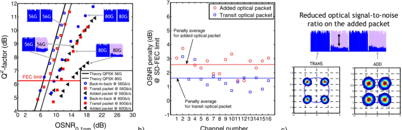
Fig. 4(a) shows the Q2-factor measurements of
a sample channel obtained when varying OSNR (measured in a bandwidth of 0.1 nm) for the output optical packet stream from the OSS node, when packets stem from the transit or add gates under switching. The switching regime means that half of the packets were blocked at each of the transit and add sides, leading to a stream of interleaved packets. For a Q2-factor of
6.25 dB, corresponding to the soft-decision forward-error-correction (SD-FEC) limit (20% overhead), OSNR sensitivities of 6.7 dB and 9.5 dB were measured respectively for 56 and 80 Gb/s data-rates in back-to-back. Comparing such sensitivities with transit packets, penalties of 0.7 and 1.5 dB were observed at 56 and 80 Gb/s, respectively. On the other hand, for
added packets, penalties increased to 3.3 and
4.5 dB at the abovementioned data-rates under switching condition; which was attributed to the limited ER, which causes extra noise on the
added packet. All channels of the integrated SB
were evaluated with 56 Gb/s QPSK optical
packets. Less than 2.6 dB and 1.7 dB average channel-to-channel OSNR sensitivity penalties were obtained respectively for the added and
transit packets (Fig. 4(b)). The constellations for
the transit and added optical packets are presented in Fig. 4(c) and show that the limited ER of the SB did impact the integrity of the optical signal on the added packet.
Conclusions
We demonstrated a novel fully integrated silicon-photonics based slot-blocker including 2 AWGs, 16 VOAs and 2 vertical fiber couplers. We showed the good performance of the device which performs wavelength demultiplexing and multiplexing, and high-speed switching (ns timescale). We integrated the SB into a packet-switched network testbed with 56 and 80 Gb/s QPSK optical packets and demonstrated a switching operation over all 16 channels. Our result constitutes an important milestone toward a fully integrated switching fabric. Further extinction ratio improvements are expected by increasing the VOA section length and the doping concentration.
Work supported in part by CELTIC+ SASER project.
References
[1] Y. Pointurier et al., "Dimensioning and energy efficiency of multi-rate metro networks," IEEE/OSA Journal of Lightwave Technology, vol. 30, no. 22 (2012).
[2] Q. Wei et al., “Multicast in Mobile Backhaul with Optical Packet Ring,” in Proc. ST-WiMob (2013).
[3] N. Calabretta et al., “On the performance of a large-scale optical Packet switch under realistic data center traffic,” Opt. Commun. Netw., Vol. 5, No. 6 (2013). [4] H.-W. Chen et al., “Forty Gb/s hybrid silicon
Mach-Zehnder modulator with low chirp,” Optics Express, vol.
19, no. 2 (2011).
[5] W. Zhang et al., “Broadband Silicon Photonic Packet-Switching Node for Large-Scale Computing Systems,” IEEE photon. Technol. Lett., vol. 24, no. 8, (2012). [6] H. Nishi et al., “Monolithic Integration of a Silica-based
Arrayed Waveguide Grating Filter and Silicon Variable Optical Attenuators based on p-i-n Carrier-Injection Structures,” in Proc. ECOC, paper We.8.E.3 (2010).
a) b) c)
Fig. 4:(a) BER measurements considering the transit and the added optical packets at 56 and 80 Gbit/s. (b) Impact of the
channel on the transit and the added optical packets at 56 Gbit/s. (c) Constellation after crossing the silicon-based slot blocker. 0 2 6 10 14 18 22 26 30 4 5 6 7 8 9 10 11 12 OSNR0.1nm (dB) Q 2 -f a c to r ( d B ) Theory QPSK 56G Theory QPSK 80G Back-to-back @ 56Gb/s Transit packet @ 56Gb/s Added packet @ 56Gb/s Back-to-back @ 80Gb/s Transit packet @ 80Gb/s Added packet @ 80Gb/s FEC limit 56G 56G 80G 80G 56G 56G 80G 80G 1 2 3 4 5 6 7 8 9 10111213141516 -1 0 1 2 3 4 5 6 7 Channel number O S N R pe nalt y (dB ) @ SD -F EC l im it
Added optical packet Transit optical packet
Penalty average for added optical packet
Penalty average for transit optical packet
-2 -1 0 1 2 -2 1.5 -1 0.5 0 0.5 1 1.5 2 ADD -2 -1 0 1 2 -2 -1.5 -1 -0.5 0 0.5 1 1.5 2 TRANS
Reduced optical signal-to-noise ratio on the added packet