HAL Id: tel-02052920
https://hal-cea.archives-ouvertes.fr/tel-02052920
Submitted on 28 Feb 2019HAL is a multi-disciplinary open access archive for the deposit and dissemination of sci-entific research documents, whether they are pub-lished or not. The documents may come from teaching and research institutions in France or abroad, or from public or private research centers.
L’archive ouverte pluridisciplinaire HAL, est destinée au dépôt et à la diffusion de documents scientifiques de niveau recherche, publiés ou non, émanant des établissements d’enseignement et de recherche français ou étrangers, des laboratoires publics ou privés.
Radio-Frequency Contact for the ITER Ion Cyclotron
Resonance Heating Antenna
Zhaoxi Chen
To cite this version:
Zhaoxi Chen. Mechanical and Materials Development of Radio-Frequency Contact for the ITER Ion Cyclotron Resonance Heating Antenna. Electromagnetism. l’Université Toulouse 3 - Paul Sabatier, 2018. English. �tel-02052920�
THÈSE
En vue de l’obtention du
DOCTORAT DE L’UNIVERSITÉ DE TOULOUSE
Délivré par l'Université Toulouse 3 - Paul Sabatier
Présentée et soutenue par
Zhaoxi CHEN
Le 6 novembre 2018Développement d'un contact Haute-Fréquence pour les
antennes à Résonance Cyclotronique Ionique d'ITER :
validation mécanique et matériaux
Ecole doctorale : SDM - SCIENCES DE LA MATIERE - Toulouse Spécialité : Sciences et Génie des Matériaux
Unité de recherche :
CIRIMAT - Centre Interuniversitaire de Recherche et d'Ingénierie des Matériaux
Thèse dirigée par
Viviane TURQ et Julien HILLAIRET
Jury
Mme Cécile LANGLADE, Rapporteur M. Mauro TABORELLI, Rapporteur
M. Jean DENAPE, Examinateur M. Olivier PASCAL, Examinateur M. Philippe DJEMIA, Examinateur Mme Viviane TURQ, Directeur de thèse
THÈSE
En vue de l’obtention du
DOCTORAT DE L’UNIVERSITÉ DE TOULOUSE
Délivré par l'Université Toulouse 3 - Paul Sabatier
Présentée et soutenue par
Zhaoxi CHEN
Le 6 novembre 2018Mechanical and Materials Development of Radio-Frequency
Contact for the ITER Ion Cyclotron Resonance Heating Antenna
Ecole doctorale : SDM - SCIENCES DE LA MATIERE - Toulouse Spécialité : Sciences et Génie des Matériaux
Unité de recherche :
CIRIMAT - Centre Interuniversitaire de Recherche et d'Ingénierie des Matériaux
Thèse dirigée par
Viviane TURQ et Julien HILLAIRET
Jury
Mme Cécile LANGLADE, Rapporteur M. Mauro TABORELLI, Rapporteur
M. Jean DENAPE, Examinateur M. Olivier PASCAL, Examinateur M. Philippe DJEMIA, Examinateur Mme Viviane TURQ, Directeur de thèse
Acknowledgment
First of all, I would like to express my sincere thanks to my thesis director Dr. Viviane TURQ and thesis supervisor Dr. Julien HILLAIRET, who were providing their enthusiastic help during the past three years. Dr. Viviane TURQ and Dr. Julien HILLAIRET are knowledgeable experts in tribology and RF engineering. With their patient guidance, I enriched my knowledge in material science and finished my Ph.D. study in material field successfully. For me, they are more than my thesis director and supervisor, they are also my mentors of life. The research and working attitude that I learned from them will benefit me all my life. It’s really my honor to be their Ph.D. student.
I would like to show my special thanks to Prof. Yuntao SONG, who is my master director and the co-director of ASIPP-CEA associated laboratory. Without his help, I may have no chance to study and work in CEA and ITER. I was deeply infected and inspired by his passion for work. Prof. SONG can always give me constructive suggestions and encourage me to conquer difficulties.
I would like to thank Dr. Caroline HERNANDEZ, Mr. Karl VULLIEZ who had the first discussion about material characterization with me and helped me to make the test planning for my first-year study. Their encouragement during these years is really important for me to finish my Ph.D. study successfully.
I would like to sincerely thank the two thesis reviewers Prof. Cécile LANGLADE and Dr. Mauro TABORELLI and jury members: Prof. Jean DENAPE, Prof. Olivier PASCAL and Prof. Philippe DJEMIA, thanks for their time and carefully review work towards my thesis. The thesis was improved significantly based on their useful comments.
I would like to acknowledge the laboratory, department and group heads: Dr. Alain BECOULET, Mr. Philippe MAGAUD, Mr. Jean-Michel BERNARD, and Dr. Tuong HOANG. Especially Mr. Jean-Michel BERNARD and Dr. Tuong HOANG, they made a lot of effort for the funding application of my Ph.D. subject and my future career after my Ph.D. graduation.
I am grateful to all the colleagues who were working with me during these three years at CEA, CIRIMAT, ASIPP and LICP: Xiaolan ZOU, Gilles LOMBARD, Patrick MOLLARD, Robert VOLPE, Walid HELOU, Fabien FERLAY, Raphael LALOO, Pierre-Louis TABERNA, Julien WAGNER, Sandrine DULUARD, Marie-Claire BARTHELEMY, Benjamin DUPLOYER, Jean-Jacques DEMAI, Hui SHAO, Kun LU, Qingxi YANG, Yong CHENG, Xuebing PENG, Prof. Peng WANG and Li QIAO.
Last by most importantly, I would like to express my deepest thanks to my parents, my three sisters and my girlfriend, thanks for their permanent love, understanding and unreserved support.
20/12/2018
CEA, Cadarache
Acronyms
AC: Alternating Current
AE: Acoustic Emission
a-C: amorphous Carbon
CoF: Coefficient of Friction
CTE: Coefficient of Thermal Expansion
CEA: Commissariat à l’énergie atomique et aux énergies alternatives
DC: Direct Current
DLC: Diamond-Like Carbon
EDS: Energy-Dispersive Spectrometer
FEM: Finite Element Method
FWHM: Full-Width at Half-Maximum FM: Front Modules
FCC: Face-Centered Cubic FFT: Fast Fourier Transform GLC: Graphite-Like Carbon HTC: Heat Transfer Coefficient
HRTEM: High-Resolution Transmission Electron Microscopy
HV-MTEST: Heatable Vacuum Material Tribological & Electrical Study Testbed HCP: Hexagonal Close-Packed
IACS: International Annealed Copper Standard
ITER: International Thermonuclear Experimental Reactor ICRH: Ion Cyclotron Resonance Heating
JET: Joint European Tokamak LHC: Large Hadron Collider LSV: Linear sweep voltammetry
OFHC: Oxygen-Free High Conductivity PVD: Physical Vapor Deposition
PP: Port Plug
Rc: Contact Resistance
RVTL: Removable Vacuum Transmission Lines RF: Radio-Frequency
SEM: Scanning Electron Microscopy TSL: Turbiscan stability index TL: Transmission Lines
TEM: Transmission Electron Microscopy XPS: X-ray Photoelectron Spectroscopy XRD: The X-ray Diffraction
Résumé
L’objectif du projet ITER est de démontrer la faisabilité scientifique et technique de la fusion nucléaire à des fins énergétiques. Pour obtenir les réactions de fusion, un plasma chauffé à 150 millions de degrés doit être confiné par un champ magnétique de plusieurs teslas en quasi-continu. Pour obtenir ces températures, des antennes radiofréquences (RF) injectent des ondes électromagnétiques de forte puissance dans le plasma, en particulier entre 40 et 55 MHz aux fréquences de résonance cyclotron des ions. L’assemblage et la dilatation thermique en fonctionnement de ces antennes sont rendus possibles par des contacts électriques glissants. Ces contacts doivent supporter un courant RF crête de 2.25 kA en régime stationnaire, dans un environnement sous vide et pendant toute la durée de fonctionnement de l’antenne. De plus, les matériaux de ces contacts doivent être compatibles avec la température de 250°C utilisée pour l’étuvage de la machine pendant plusieurs milliers d’heures cumulées. Ces contacts RF sont donc des composants critiques pour les performances de l'antenne. Aucun contact électrique du commerce n'a jusqu'à présent été qualifié pour ces spécifications et un effort particulier a donc été porté dans le cadre de ce travail de thèse afin de développer une solution satisfaisante.
Le choix des matériaux et des revêtements utilisés pour ces contacts a fait l’objet de la première partie de cette étude. Pour ce faire, un modèle multi-physique tenant compte des paramètres RF, mécaniques et thermiques a été développé. À la suite de cette étude, des premiers couples de matériaux et de revêtements ont été sélectionnés. Les propriétés d’échantillons représentatifs ont été caractérisées par des mesures réalisées au laboratoire CIRIMAT avant et après un vieillissement thermique simulé.
Afin d’évaluer le comportement électrique et tribologique de ces paires de matériaux dans les conditions de fonctionnement d’ITER, un tribomètre sous vide a été spécifiquement conçu et utilisé pendant ce travail de thèse. Ce tribomètre permet de mesurer l’évolution du coefficient de frottement et de la résistance de contact entre deux échantillons en mouvement relatif linéaire, sous vide (10-5 Pa) et jusqu’à 350°C. Des couples d’échantillons de 316L/CuCrZr non revêtus ont été comparés à des couples revêtus d’argent et de rhodium ou d’or et de rhodium. La force normale de contact optimale a d’abord été déterminée par rapport à la résistance de contact et au coefficient de frottement. L’évolution dynamique de ces paramètres et la durée de vie des revêtements ont ensuite été mesurées sur le cycle de vie attendu des contacts de l’antenne ICRH d’ITER.
Enfin, la faisabilité d’une nouvelle méthode de lubrification compatible avec le vide a été développée à partir de revêtements composites or/nickel/carbone et or/cobalt/WS2.
Ces nouveaux revêtements ont été élaborés par des méthodes de dépôt en phase vapeur et d’électrodéposition respectivement. Leurs performances tribologiques ont été caractérisées dans des conditions représentatives de celles d’ITER.
ABSTRACT
Ion Cyclotron Resonance Heating (ICRH) is one of the most important plasma heating methods in magnetically confined fusion experiments. In ITER, two ICRH antennas are designed to supply 20 MW of Radio-Frequency (RF) power at 40-55 MHz to heat the plasma. RF sliding contacts are used in the antennas to allow their remote handling assembly and to improve their maintainability, as well as to absorb the thermal expansion of the RF conductors during operations. One of the RF contacts is designed to be operated at 2.25 kA in steady-state (1200 s), with a current density of 4.8 kA/m. With such current levels, high heating occurs at the contact area which threatens the structural and material safety of the RF contacts and constrain their life time. In addition, before operation of the ITER ICRH antennas, all the in-vessel structures will be baked at 250°C during thousands of cumulated hours for outgassing.
In CEA, R&D work on RF contact development has been carried out for 10 years. Recently, Ag-coated CuCrZr louvers RF contact prototype based on Multi-Contact LA-CUT commercial contact configuration was tested on TITAN test-bed. 1500 A, 1200 s steady-state operation was achieved. However, due to burn failure, the RF contact prototype couldn’t reach 1200 s steady-state under 2 kA as expected. In order to improve the performances of the RF sliding contacts to match ITER requirements, failure mechanisms of RF contacts during RF operations were analyzed and possible materials or coated systems that can be used for RF sliding contacts compatible with the ITER environment have been studied in detail within this thesis work. The effects of material selection, cooling parameter and contact resistance on louvers temperature have been modelled and simulated through finite element methods.
Moreover, functional coatings like Ag, Au, Rh and their alloys were manufactured by electroplating on 316L and CuCrZr, which are commonly used as base materials on tokamak. By mimicking the ITER baking conditions, the coated samples were thermal aged under vacuum at 250ºC for 500 h, after which the materials properties evolution such as hardness, grain size and adherence was characterized. In addition, the coating life time has been evaluated through cross-sectional diffusion characterizations.
In order to evaluate the electrical and tribological behavior of the coated material pairs, a dedicated and innovative test bed was designed during this thesis and used successfully. On this test bed the samples can be heated up to 350ºC and the vacuum can reach 10-5 Pa. Static contact resistance as well as transient contact resistance/friction coefficient of sliding pairs can be measured. Sliding and electrical tests of uncoated 316L/CuCrZr pair and coated pairs Ag/Rh and Au-Ni/Rh were
carried out. The relationships between vacuum condition, temperature, contact force and the static contact resistance have been studied and an optimal contact force was selected. Under this optimal contact force, the sliding tests were launched and the evolutions of friction coefficient as well as contact resistance were analyzed. Through wear characterizations, the life times of the coatings were evaluated.
Finally, based on the first tribological results obtained on commercial Au-Ni and Au-Co alloy coatings, the feasibility of depositing solid lubricant containing Au-Ni and Au-Co composite coatings to minimizing wear and friction coefficient was evaluated. Au-Ni/a-C and Au-Co/WS2 composite coatings were successfully
developed by using magnetron sputtering and electroplating methods respectively. Their tribological performance under ITER relevant vacuum condition had been studied.
Contents
Chapter 1 Context and objectives ... 1
1.1 Energy and nuclear fusion ... 1
1.1.1 Global Energy Situation ... 1
1.1.2 Nuclear fusion ... 1
1.2 ITER and ITER ICRH antenna ... 2
1.2.1 Magnetic confined fusion and Tokamak ... 2
1.2.2 ITER project ... 3
1.2.3 ITER ICRH antenna and RF contacts ... 4
1.2.3.1 Mechanical design of ICRH antenna ... 4
1.2.3.2 RF contact design specifications ... 5
1.2.3.3 RF contact design challenges ... 6
1.3 RF sliding contact development status ... 6
1.4 Research aims and objectives ... 8
Chapter 2 Coating deposition and characterization techniques ... 11
2.1 Coating deposition techniques ... 11
2.1.1 Overview ... 11
2.1.2 Electroplating ... 12
2.1.2.1 Faraday’s Law ... 12
2.1.2.2 Main factors that affect electroplating process ... 13
2.1.3 Magnetron sputtering deposition ... 14
2.2 Characterization techniques ... 14 2.2.1 3D optical profiler ... 15 2.2.2 SEM/EDS ... 15 2.2.3 TEM ... 16 2.2.4 Micro-scratch tester ... 17 2.2.5 Nanoindentation tester ... 18 2.2.6 Microharness tester ... 19 2.2.7 XRD ... 19
2.2.8 XPS ... 20
2.2.9 Raman spectroscopy ... 21
2.3 Tribology of conductive contact ... 22
2.3.1 Electrical contact resistance ... 22
2.3.2 Friction and wear ... 26
2.3.2.1 Source of friction ... 26
2.3.2.2 Wear ... 26
2.3.2.3 Lubrication ... 28
2.4 Tribological study tools ... 30
2.4.1 Tribometer configuration and parameters ... 30
2.4.2 Ball on disc tribometers ... 31
2.4.3 Pin on plate ITER RF contact specific tribometer ... 32
2.4.3.1 System design ... 32
2.4.3.2 Modeling and simulations results ... 39
2.4.3.3 Calibration of the CoF measurement system ... 44
2.4.3.4 Precision Measurements ... 45
2.4.4 Overview of tribological test parameters ... 49
Chapter 3 Experimental study and failure analysis of Multi-Contact LA-CUT contact ... 51
3.1 ITER RF sliding contact prototype design ... 51
3.1.1 RF sliding contact configuration selection ... 51
3.1.2 Base material selection for the RF contact ... 53
3.2 RF tests of LA-CUT prototype ... 54
3.2.1 T-Resonator Setup ... 55
3.2.2 RF Contact holder ... 56
3.2.2.1 RF contact holder design... 56
3.2.2.2 Thermal-hydraulic analysis ... 57
3.2.3 LA-CUT prototype RF test results ... 61
3.2.4 LA-CUT RF contact failure analysis ... 63
3.2.5.1 Theoretical model ... 66
3.2.5.2 Finite element analysis model ... 67
3.2.5.3 Analysis procedure and results ... 67
3.3 Discussion ... 71
Chapter 4 Thermal stability, electrical and tribological characterization of coatings ... 73
4.1 Materials and samples preparation ... 73
4.1.1 Material selection ... 73
4.1.1.1 Au and Au alloys ... 74
4.1.1.2 Ag and Ag alloys ... 74
4.1.1.3 Rhodium ... 75
4.1.2 Sample manufacturing ... 75
4.1.3 Characterizations and sample preparation ... 76
4.1.3.1 Thermal aging process ... 76
4.1.3.2 Tests planning ... 77
4.2 Characterization results of thermal stability ... 78
4.2.1 Coating properties changes and diffusion with substrate ... 78
4.2.1.1 Au-Ni on CuCrZr ... 78
4.2.1.2 Ag-Sb on CuCrZr ... 86
4.2.1.3 Rh on CuCrZr ... 89
4.2.1.4 Rh on 316L ... 95
4.2.2 Diffusion between coatings ... 99
4.2.2.1 Au-Ni on CuCrZr vs. Rh on 316L ... 99
4.2.2.2 Au-Ni on CuCrZr vs. Rh on CuCrZr ... 100
4.2.2.3 Ag-Sb on CuCrZr vs. Rh on 316L ... 101
4.2.2.4 Ag-Sb on CuCrZr vs. Rh on CuCrZr ... 102
4.2.3 Discussion ... 102
4.3 Electrical/tribological characterizations under ITER relevant conditions ... 103
4.3.1 CuCrZr vs. 316L ... 103
4.3.1.2 Evolution of Rc and CoF during sliding cycles ... 105
4.3.1.3 Wear surface morphology ... 106
4.3.2 Au-Ni on CuCrZr vs. Rh on 316L ... 107
4.3.2.1 Static contact resistance ... 107
4.3.2.2 Evolution of Rc and CoF during sliding cycles ... 108
4.3.2.3 Wear surface morphology ... 108
4.3.3 Au-Ni on CuCrZr vs. Rh on CuCrZr ... 110
4.3.3.1 Evolution of Rc and CoF during sliding cycles ... 110
4.3.3.2 Wear surface morphology ... 111
4.3.4 Ag on CuCrZr vs. Rh on 316L ... 112
4.3.4.1 Static contact resistance ... 112
4.3.4.2 Evolution of Rc and CoF during sliding cycles ... 112
4.3.4.3 Wear surface morphology ... 113
4.3.5 Ag on CuCrZr vs. Rh on CuCrZr ... 114
4.3.5.1 Evolution of Rc and CoF during sliding cycles ... 114
4.3.5.2 Wear surface morphology ... 114
4.3.6 Discussion ... 115
Chapter 5 Self-lubricating coating development ... 117
5.1 Au-Ni/a-C deposition and coating characterizations ... 117
5.1.1 Magnetron sputtering process of Au-Ni/a-C ... 117
5.1.2 Coating characterizations ... 118
5.1.2.1 Surface morphology ... 118
5.1.2.2 Coating composition and crystal structure ... 119
5.1.2.3 Mechanical performance ... 123
5.1.2.4 Electrical performance ... 126
5.1.2.5 Tribological performance ... 127
5.1.3 Summary ... 128
5.2 Au-Co/WS2 deposition and coating characterizations ... 129
5.2.1.1 Ni interlayer plating ... 129
5.2.1.2 Au-Co/WS2 plating ... 133
5.2.2 Coating characterizations ... 140
5.2.2.1 Coating composition ... 140
5.2.2.2 Coating morphology and topography ... 141
5.2.2.3 Crystal structure ... 144
5.2.2.4 Tribological performance ... 145
5.2.2.5 Summary ... 148
5.3 Tribological performance comparison of different coatings ... 149
5.4 Discussion ... 150
Chapter 6 Conclusions and prospect ... 153
6.1 Conclusions of this thesis ... 153
6.2 Future work ... 155
References ... 157
Appendix A: HV-MTEST Plotting Methods ... 173
Appendix B: Binary phase diagram ... 175
Appendix C: Investigation of the generation of the top layer ... 181
1
Chapter 1 Context and objectives
1.1 Energy and nuclear fusion
1.1.1 Global Energy Situation
Energy sources are fundamental for human society and the global energy consumption is increasing rapidly nowadays. Currently, available world energy resources are based mostly on fossil fuels such as coal, oil and gas. However, as un-renewable sources, fossil fuels can run out in the future and the pollution caused by their consumption is a serious problem. In the past decades, renewable energy sources such as wind and solar energy were widely studied and applied all over the world. Although renewable energy sources are replacing part of traditional fossil fuels role, their intermittent natures let them impossible to fully satisfy the world's energy requirements.
Nuclear fission was first investigated and explained in the late 1930's and the first commercial fission power plant was built in the 1950’s. As a reliable and high efficiency energy source, nuclear fission is well developed in many countries. In France for instance, 78% of electricity is generated from fission power plants. After the Fukushima Daiichi accident on 11 March 2011 that was caused by an earthquake and a subsequent tsunami, several countries with operational nuclear power plants decided to phase-out the use of the technology over the next two decades [1]. Due to the high safety risk of radioactive pollution caused by accidents of fission power plants, the fever of fission energy application cold down all over the world. Therefore, energy sources that can offer safe and renewable energy still have to be found.
1.1.2 Nuclear fusion
2
Nuclear fusion is another nuclear reaction which is happening in stellar cores. In the fusion process, the nuclei are fused together and release energy. On earth, the technically easiest achievable nuclear fusion reaction is the fusion between hydrogen isotopes deuterium (D) and tritium (T) due to their high cross-section and the greatest yield of energy per reaction (Figure 1-1).
The fusion reaction of deuterium and tritium is expressed as:
2 3 4 1
1
D
1T
2He
0n
17.6
MeV
(1-1)In order to achieve fusion reactions between deuterium and tritium, one has to bring the nuclei (which are positively charged) close enough (<10-15 m) to overcome the electrostatic repulsion, so that the nuclear strong force can bind the nucleons together in a nucleus[3, 4]. In practice, the D-T nuclei should be heated to about 100 million Kelvin, which is much higher than the ionization temperature of the hydrogen atom which is in the order of 10000 K. In other words, the fusion reaction can only occur in a fully ionized plasma state.
Compared with nuclear fission, the nuclear fusion reaction itself does not produce radioactive wastes. Moreover, since the Deuterium isotope can be found in abundance in seawater and the Tritium could be generated from the interaction of the high energy neutron with Lithium, fusion energy would have no shortage of fuels. All these advantages make fusion energy a candidate for the future energy supply and fusion development is carried out in many countries all over the world.
1.2 ITER and ITER ICRH antenna
1.2.1 Magnetic confined fusion and Tokamak
Figure 1-2 Diagram of ions and electrons trajectories in a DC magnetic field
3
Kelvin. The idea is to use a magnetic field to trap the charged plasma particles in order to control the contact with the wall of the container. In a steady magnetic field, electrically charged moving plasma particles move in spiral orbits along magnetic field lines (Figure 1-2). Trapping the plasma particles along the magnetic field lines has been successfully achieved by some magnetic confinement concepts, such as reversed field pinch, stellarator and tokamak.
In the world, tokamak has been the most developed magnetic confinement system and is presently the basis for a future fusion reactor design in many countries [5-7]. As shown in Figure 1-3, plasma is contained in a torus-shaped vacuum vessel and confined by a specially designed magnetic field configuration [8]. A set of Toroidal Field (TF) coils are installed along the torus to generate the toroidal magnetic field. However, toroidal field is not sufficient to confine the plasma alone, due to the curvature of the magnetic field lines which produces opposite particle drifts for ions and electrons. Due to this particle drift, plasma shifts rapidly toward the wall and gets lost. In order to avoid this particle drift phenomenon, an additional poloidal magnetic field is necessary, which combines with the toroidal field and forms spiral magnetic lines. The poloidal magnetic field is generated by a flowing current in the plasma, magnetically induced by the inner poloidal field coils. In addition, External Poloidal Field (PF) coils are designed for plasma positioning and shaping.
Figure 1-3 Schematic of tokamak [9]
1.2.2 ITER project
In the past 50 years, tokamak-based magnetic confinement fusion research achieved impressive progress: on JET and TFTR tokamaks, total fusion powers of 16MW and
4
11MW were produced respectively [10]. However, based on confinement scaling laws, in order to generate enough power to sustain the fusion reaction itself, the size of the machine should be enlarged almost twice as large as any tokamak machine existing. So, large size tokamak machine needs to be built to get further progress.
In order to demonstrate the scientific and technological feasibility of fusion energy, the ITER Project was launched in 1988. As an international project, China, the European Union, India, Japan, Korea, Russia and the United States firmly committed to building the International Thermonuclear Experimental Reactor (ITER), which is the world largest tokamak[10-12].
The primary objectives of ITER tokamak are 1). achieving the out-versus-in power amplification ratio of the fusion reaction (Q) no less than 10 and generating 500MW output power for 400 s. Thus, ITER will be the first machine that could gain net energy after subtracting the energy to initiate the fusion reaction. 2). to demonstrate steady-state operation non-inductive current drive at Q ≥ 5. 3). to demonstrate availability and integration of essential fusion technologies. 4). to test components for a future power reactor including high temperature tritium breeding blanket module concepts with the 14 MeV neutron power load.
1.2.3 ITER ICRH antenna and RF contacts
To heat the deuterium and tritium fuel to fusion temperatures, ITER relies in part on Ion Cyclotron Resonance Heating (ICRH) power. ITER ICRH system is one of the three heating systems that are anticipated to be used during plasma experiments and two antennas will be installed in ITER equatorial ports with a total heating power of 20 MW (40-55 MHz) up to one-hour steady-state operation for a variety of ITER plasma scenarios [13-16].
1.2.3.1 Mechanical design of ICRH antenna
As shown in Figure 1-4, each of the ITER ICRH antennas was designed as port plug structure with a total weight of 45 tons [14]. In order to ease the assembly, each port plug was split into four symmetric pieces in a 2×2 array. In the front of the port plug (PP), front modules (FM) transfer and couple the RF power to ITER plasma. This RF power is generated by sources that will be installed far from the ITER machine and transferred through transmission lines (TL). In the port plug, there are eight removable vacuum transmission lines (RVTL) designed to connect the FM and TL [17]. The RVTL has been designed to be maintained or replaced using remote handling system without extracting all the heavy and complex PP. For the RF plasma coupling adjusting consideration, a shimming process has also been foreseen to allow
5
FM radial displacement of few centimeters relative to the RVTL [14, 15]. Besides, due to uniform temperature distribution, large thermal stress can generate inside the RVTL, which will threaten the RVTL’s structural safety.
Figure 1-4 Overview of ITER ICRH antenna
To allow the relative displacement between FM and RVTL as well as to release the thermal stress in the RVTL, flexible connection joints named RF contacts were added at some different locations. The most stringent operation conditions of three of these RF contacts are reported in Table 1-1.
Table 1-1 General parameters of the three locations' RF contact on the ITER ICRH
Contact Max IRF [kA] Diam. [mm] Max JRF [kA/m]*
#1 : 2.0 140 4.6
#2 : 2.5 260 3.1
#3 : 2.3 218 3.4
(* The current density is defined as JRF= IRF/π∙Diam.)
1.2.3.2 RF contact design specifications
These contacts must satisfy the following constraints:
The RF contact (#3) should work normally under 2.25 kA (+20% of safety margin) at 40-55 MHz for 1200 s steady-state operation without any failure.
The structural and material of the RF contact should be compatible with the ITER vacuum condition which is a pressure lower than 10-4 Pa.
The RF contact should sustain high temperature baking at 250°C during ITER baking phase for 2×10⁴ hours without structure problem caused by creeping
6
and diffusion.
The RF contact should sustain linear sliding under two sliding modes: thermal expansion happens during RF operation and baking or insertion during assembly. For the first mode, based on the calculation, the sliding speed is 0.05 mm/s with a sliding stroke of 2 mm. For the assembly insertion, the total stroke is about 50 mm and the speed is 1 mm/s-5 mm/s (should be compatible with the remote handling system).
1.2.3.3 RF contact design challenges
Based on the relative motion between electrical contact parts, electrical contacts can be divided in general into two basic types: stationary contacts and moving contacts[18]. According to the property of current that flows through, electrical contacts can be classified as direct current (DC) contacts and alternating current (AC) contacts. ITER RF contacts are sliding contacts that will work under a heavy current load with a current frequency of 40-55 MHz.
One of the bigest challenges for the ITER ICRH RF contact design is the large current or current density (4.6 kA/m Max.) which will induce large thermal load, especially at contact areas due to Ohmic loss, where the contact resistance generated. Even if active cooling is designed below the RF contact, confined by the flexible RF contact's mechanical design, the distance between the contact to the cooling channel can be few centimeters and the cooling efficiency reduced. During steady-state operation, heat will accumulate and temperature will increase which would induce structure and material failures. For this reason, the mechanical structure design and contact material selection which can ensure the function stability are the most important aspects. Compared with stationary electrical contacts, sliding contacts are facing much critical working conditions: severe wear and corrosion. Moreover, the RF condition makes the sliding contact design more challenging, as “skin effect” increases the bulk resistance, thus increases the Ohmic loss accordingly.
1.3 RF sliding contact development status
Although RF contacts are commonly used in the electronic industry as well as on scientific research facilities, however, their application on high RF current load under vacuum is very limited. Before the RF sliding contact development for fusion applications, almost no research experience existed regarding such components. Commercial RF contact LA-CUT produced by the Multi-Contact® company (now part of Stäubli) [19] was selected as a possible design concept for various ICRH systems, in particular for ITER [20]. During the last 15 years, such contacts have been
7
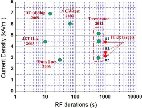
tested in various operating conditions in IPP [21] or CEA [22] and are currently used in the JET ICRH ITER-like antenna [23]. The experiments results obtained at CEA under vacuum are summarized in Figure 1-5.
Figure 1-5 Summary of Multi-Contact LA-CUT RF experiment results in CEA
CEA started to investigate the electrical performance and reliability of flexible finger contacts since 2002. The first RF sliding contact prototype was designed based on the Multi-Contact LA-CUT configuration and installed in the JET-EP ITER-like antenna to provide a separable electrical coupling between tuning capacitors and current straps [22]. In this work, Multi-Contact LA-CUT had been tested under vacuum condition, up to 36 kV and 1.75 kA peak (1.24 kA RMS) during 10 s with a current density around 4.5 kA/m. In 2004, these same contacts were successfully tested for 60 s steady state operation under the current density of 6.16 kA/m in vacuum at 59 MHz. The feasibility of applying Multi-Contact LA-CUT commercial RF contact in ITER vacuum condition was proved.
In 2009, Multi-Contact LA-CUT contact was tested in a vacuum environment up to 60 s. Moreover, sliding tests were first performed to investigate the feasibilities of contact sliding during RF shot [24]. The mock-up consists of a Φ54 mm strip holder, where louvers faced a thick 500 µm copper electroplated steel part. During the mechanical sliding test, the abrasion on the copper plated part was so serious that the sliding was blocked due to wear debris generated. At last, the copper coated cylinder was changed to CuCr (with higher hardness than copper) and wear problem solved. Based on this prototype, RF tests had been performed at 57 MHz up to 32 kV / 1.2 kA peak (7.07 kA/m) under vacuum during 16 s with a sliding speed of 5 mm/s over a
8
50 mm range. From this test, the capability of Multi-Contact LA-CUT to support RF operation during sliding was demonstrated. But its steady state operation capability still required further investigations.
For that purpose, RF tests have been performed on Multi-Contact LA-CUT under vacuum on a newly developed facility (T-resonator), which is a dedicated testbed for ITER RF components development. These contacts have been tested under 2 kA/600 s (4.54 kA/m) and ultimately up to 2.28 kA (5.18 kA/m) peak during 600 s at 62 MHz on both a Φ140 mm holders, after which the contact band was destroyed (Figure 1-6).
Figure 1-6 Multi-Contact LA-CUT RF contact before and after RF tests1
Even though significant progress about the mechanical design of RF sliding contacts and the necessary knowledge about their material had been achieved in the previous R&D phase, there is still a large gap between the obtained results and the ITER RF sliding contact design specifications.
1.4 Research aims and objectives
The development of an ITER RF sliding contact is the combination of mechanical structure design and material selection. The previous studies [21-24] mainly focused on the RF current carrying capability of the LA-CUT commercial product. However, the failure mechanism of the RF contact was not deeply researched. As a result, the main parameters or factors that can affect the RF contact’s stability were not clearly understood.
1
I would like to add that LA-CUT is a widely used and high-tech commercial electrical contact. It was not designed specifically for ITER application. In this thesis study, LA-CUT was selected to test under ITER relevant conditions. The failure presented in this figure doesn’t present the quality of the LA-CUT product and the test results are significantly affected by the test conditions as well as the performance of the conductor that the LA-CUT was installed in. The test conditions were out of its manufacturing specifications.
9
Meanwhile, as commercial RF contact, LA-CUT was designed mainly for civil (and DC) applications. However, the ITER RF sliding contacts will be facing in ITER specific nuclear fusion conditions which include high vacuum, high temperature and neutron radiation. The thermal effects and metal diffusion induced by thermal aging to the materials mechanical and electrical property changes should be investigated. Besides, as a sliding electrical contact, the understanding of the tribological performance of contact materials under ITER operation conditions is also essential to direct the material selection. The neutron irradiation effects on the materials will not be investigated in this work.
The aims of this thesis are:
1) Understanding the failure mechanisms of RF sliding contacts in the context of ITER ICRH system. Creating multi-physics analysis model of the contact and analyzing the main factors and parameters that can affect the operating temperature of the RF contact louvers through Finite Element Analysis (FEA) method.
2) Selecting electrical contact materials which are expected to have good performance of electrical conductivity and wear resistivity in ITER operating conditions. Mimicking ITER high temperature baking periods and investigating the selected materials’ thermal stabilities and diffusion phenomena after thermal aging treatment at 250°C for 500 h.
3) Developing an electrical and tribological multi-functional test bed with ITER relevant conditions such as vacuum and temperature. Investigating the electrical contact and wear performance of the material pairs on the test bed and analyzing the effects of wear to the contact resistance.
4) From the acquired knowledge, designing a new ITER RF sliding contact prototype to be tested on the IRFM RF T-resonator
5) Studying the feasibility of applying advanced self-lubricating coatings on RF sliding contact to improve their wear performance in ITER. Investigating the possibility of co-depositing nanoparticles of solid lubricants (WS2, carbon)
within the electrical contact functional coatings.
In summary, in this thesis study, the failure mechanisms of the LA-CUT commercial electrical contact under ITER ICRH application conditions are expected to be investigated and the relationship between the LA-CUT operational performance with the material selection will be analyzed. Based on the material properties requirements obtained from the LA-CUT prototype failure analysis, the proper material candidates
10
(commercial and self-developed) were evaluated under ITER relevant conditions, which can give a direction to the material selection for the ITER ICRH RF sliding contact development.
Therefore, this manuscript will be divided into 5 parts: after the thesis general introduction (chapter 1), in chapter 2, the coating deposition techniques, material characterization techniques and background of wear and contact resistance were introduced. In this thesis, not only commercial material characterization tools were used, a multi-functional tribometer that can mimic ITER conditions to perform the materials’ electrical/tribological characterizations was developed during the thesis. So, the engineering details of the multi-functional tribometer development were also introduced in chapter 2. Chapter 3 introduces the RF test results and the failure mechanisms of the LA-CUT electrical contact under ITER relevant conditions. During the failure mechanism analysis, both the material characterization by commercial material characterization techniques and the FEM analysis were applied. Based on the failure mechanism analysis, CuCrZr and 316L were selected to be the base material candidates for the ITER RF conductor and CuCrZr was selected as the base material candidate for the RF contact louver. Functional coatings were also proved to be necessary which can help to improve the base materials’ electrical and tribological performance. In chapter 4, various of commercial functional coatings that were electroplated on CuCrZr and 316L substrates were evaluated under ITER relevant working conditions and wear was observed to be a problem which shortened their life time. The possibility of applying solid lubricants to improve the coatings’ wear performance was evaluated in chapter 5 by developing and testing two kinds of self-lubricating coatings. Chapter 6 will finally conclude this manuscript.
11
Chapter 2 Coating deposition and characterization techniques
ITER RF sliding contact is a critical component that has both harsh mechanical and electrical design requirements. Applying suitable coatings on proper substrates is a possible material solution. Material selection and the following characterizations in mechanical, electrical and diffusion properties are major steps for the ITER RF sliding contact development. In this chapter, the coating techniques and the coating characterization techniques (morphology, composition, mechanical properties, crystal structure) that are used in this study are introduced. The background knowledge of wear and contact resistance between coating surfaces in vacuum which can help to understand the ITER RF sliding contact’s failure mechanism is discussed. The engineering design of the dedicated testbed for coatings’ electrical and tribological performance characterization is also presented.2.1 Coating deposition techniques
The performance of an electrical contact is mainly the consequences of the phenomena occurring at its surface, such as contamination, oxidation, re-oxidation, wear, etc. [18] The above factors can increase the contact resistance so as to threaten the reliability of the connection. As a commonly used surface engineering method, applying coating is an effective practical solution for various electrical contacts, on which thin coating layers play a major role in dealing with corrosion, wear and metal diffusion. Based on the coating material’s characteristics and operating conditions, the coating thickness varies from 0.1–0.3 µm to 20–30 µm.
2.1.1 Overview
Generally speaking, the majority of contact materials that help to improve electrical contact quality, are noble metal materials. Depositing them as micron scale coatings on common structural metal materials is common practice for high-power RF components. The practical coating methods include electroplating, electroless plating, spraying and Physical Vapor Deposition (PVD). Hardness and surface quality can affect the electrical contact’s wear performance. Generally, hard coatings with smooth surfaces have higher wear resistance. Electroplating and PVD deposition methods can generate fine grain size coating, which has better hardness performance than spraying and electroless plating. Moreover, by using electroplating and PVD methods, alloy coatings and composite coatings can be achieved, which is beneficial for advanced coating development in which solid lubricant materials are expected to be co-deposited. In this thesis, two self-lubricating composite coatings were developed. The Au-Ni/C coatings were deposited by magnetron sputtering under the collaboration with Lanzhou Institute of Chemical Physics in China (discussed in
12
section 5.1). The Au-Co/WS2 coatings were electrodeposited at CIRIMAT laboratory
in France (discussed in section 5.2).
2.1.2 Electroplating
Figure 2-1 Schematic of electrodeposition
Electroplating is a process of depositing metal or conductive metal oxides thin films on conductive substrates by applying an electric current to reduce the metal cations dissolved into the electrolyte [25, 26]. A generic electroplating cell setup is shown in Figure 2-1.
There are two electrodes applied during the plating process: the anode and the cathode. The cathode is the piece to be plated and the anode is either a sacrificial anode or an inert anode (normally either platinum or carbon). For a sacrificial anode, the metal ions Mz+ are exchanged between two phases, the solid metal and the solution contains Mz+. The metallic ions in salt carry positive charges and get attracted to the cathode when passing a negative current. When they reach the surface of the cathode, it provides electrons to reduce the positively charged ions into metallic form[27, 28]. On the anode, the reaction is reversed. The reactions of electrodeposition are expressed as:
z
M
ze
M
(2-1) If the anode is an inert anode, oxygen evolution takes place at the anode:2 2
2
H
O
2
e
2
O
H
H
(2-2)2.1.2.1 Faraday’s Law
Faraday’s law states the relationship between the coating production and the quantity of electric charge passed through the electroplating cell. It’s a useful method to
13
calculate the coating thickness. The weight of coating product is:
I t M m n M z F (2-3)
where, I is the current (A), t is the coating time (s), M is the molecular weight (g/mol),
z is the number of electrons transferred, F is the Faraday constant (96487 C/mol).
The coating thickness (µm) can be calculated through:
100
k k/ 60
d
KD t
(2-4) where K is the coating metal’s electrochemical equivalent (g·A-1·h-1), Dk is the currentdensity (A/dm2), t is the coating time (min), ηk is the cathode current efficiency and ρ
is the density of the coating material (g/cm3).
2.1.2.2 Main factors that affect electroplating process
1) Temperature
Generally, increasing the temperature of the electrolyte can increase the solubility of the metal salts and improve the conductivity of the solution accordingly [27, 29]. Increasing temperature can decrease the viscosity of the solution, thereby replenishing the double layer relatively faster. Besides, with high plating temperature one can achieve low stress and low cracking tendency coating as the hydrogen absorption on the coating is decreased. However, high temperature may increase the crystal size and sometimes impairs the coating quality. So, in practice, the plating temperature is selected by compromising the deposition rate and coating quality.
2) Agitation
Agitation provides sufficient mixing of electroplating bath and replenishes metal ions at the cathode surface which reduces the thickness of diffusion layer. Under agitation, high current density can be used during the plating process to achieve high productivity. Meanwhile, agitation helps to remove hydrogen bubbles from the coating surface, which prevents voids defects in the coating [30]. Many types of stirring can be used such as mechanical swing, electric shock, gas vibration and so on.
3) Current density
In electroplating, current density plays an important role in the coating rate and coating quality. The selection of current density must take the bath composition and temperature into consideration. Insufficient current density will result in poor coating, while excessive current density may induce burn defects [31].
14
2.1.3 Magnetron sputtering deposition
Magnetron sputtering is a plasma-based deposition process in which energetic ions are accelerated towards a target. The ions strike the target and atoms are ejected or sputtered from the target surface and deposited on the substrate to generate film. Magnetron sputtering belongs to PVD deposition method.
The scheme of the J450 magnetron co-sputtering system used in this thesis study is shown in Figure 2-2. The coating substrate and target are installed in a chamber. During the plating process, a DC power supply or RF power supply is used between the target (cathode) and substrate (anode) [32, 33]. Ar plasma is generated between the electrodes and Ar+ ions are accelerated to bombard the target surface. What differentiates a magnetron cathode from a conventional cathode is the presence of a magnetic field. The magnetic field in the magnetron is oriented parallel to the cathode surface. The local polarity of the magnetic field is oriented such that E×B drift of the emitted secondary electrons forms a closed loop. Due to the increased confinement of the secondary electrons in this E×B drift loop, the ionization efficiency of Ar gas is increased and the plasma density near the target surface is increased too. With ionization of Ar gas, the energy of the electrons decreased, which eliminates the heating problem of the substrate due to electron bombardment. More deposition details are introduced in Chapter 5 (section 5.1.1).
Figure 2-2 Schematic configuration of the magnetron sputtering system
2.2 Characterization techniques
Several different techniques were used to analyze or characterize the coating materials aiming for ITER RF sliding contact development. The coatings’ morphology, coatings’ mechanical properties (adhesion, hardness and elastic modulus), coatings’ chemical
15
composition and crystal structure were characterized. The techniques used in this study include: 3D optical profiler, Scanning Electron Microscopy (SEM), Energy-Dispersive Spectrometer (EDS), Transmission Electron Microscopy (TEM), micro-scratch tester, nanoindentation tester, X-ray Photoelectron Spectroscopy (XPS), The X-ray Diffraction (XRD) and Raman spectroscopy.
2.2.1 3D optical profiler
Optical profilers are interference microscopes used to accurately measure the three-dimensional height variations on surfaces of a given test material. As Figure 2-3 shows, optical profilers manipulate the wave properties of light entering the microscope and compare the path differences between the test subject and a reference object of a known flatness. Once light enters the optical profiler, the light beam will split, where one-half of the beam reflects the focal plane of a microscope objective for the object of interest and the other half is reflected from the reference mirror. Interference between these two beams is then measured to form an interferogram from which height calculations can be obtained [34]. The main advantage of the 3D optical profiler is the non-contact measurement.
Figure 2-3 Schematic of a 3D optical profiler [35]
The 3D optical profiler (SENSOFAR, USA) was used in this thesis to measure the samples’ surface roughness.
2.2.2 SEM/EDS
The resolution of microscope is limited by the wavelength of visible light. For large magnification images, light or particles with shorter wavelength is mandatory.
16
Electrons have shorter wavelengths; therefore in electron microscopy larger magnifications, up to two million times, become possible [36]. Based on electron microscopy, SEM was developed which is a widely used technique to study the surface morphology and compositional distribution. As Figure 2-4 shows, the tested sample is introduced into a vacuum chamber where a focused beam of electrons interacts with the sample. The primary electrons interact with the surface atoms producing several detectable signals, among which backscattered electrons, secondary electrons and X-rays are used the most for the analysis. Secondary electrons give information about the surface morphology. From backscattered electrons, the elements with high atomic number Z will appear lighter than the elements with a low Z. So, they can supply composition information. The number and energy of the X-rays emitted from a specimen can be measured by an EDS. As the energies of the X-rays are characteristic of the elements that emitting such X-rays. X-rays detection gives additional insight into the elemental composition of the surface.
In this thesis, JSM-6510LV (JEOL, Tokyo, Japan), JSM-6700F FEG-SEM (JEOL, Tokyo, Japan) and JSM-5601(JEOL, Tokyo, Japan) were used to study the surface morphology and composition of the coating surfaces as well as wear tracks.
Figure 2-4 Schematic diagram of SEM system [37]
2.2.3 TEM
TEM is used to produce images from a sample by illuminating the sample with electrons beams within a high vacuum and detecting the electrons that are transmitted
17
through the sample. The TEM operates on the same basic principles as the light microscope but uses electrons instead of light. As the De Broglie wavelength of electrons is much smaller compared with visible light, the optimal resolution attainable for TEM images is significantly higher than optical microscopes, which reaches to 1nm [38].
TEM is a powerful tool for nanoparticle characterization and can be applied to study crystal structure and features in the structure like dislocations and grain boundaries. There are two modes in TEM, the imaging mode and the diffraction mode. In imaging mode, the darker areas of the image represent areas of the sample where fewer electrons are transmitted through, while the lighter areas of the image represent the areas of the sample where more electrons were transmitted through. The diffraction mode is a useful tool for doing a cell reconstruction and determining crystal orientation.
HRTEM images of the coating cross-sections were captured by using TECNAI G2 F20 S-TWIN (FEI, USA) instrument at an accelerating voltage of 200 kV equipped with EDS unit. Cross-sectional samples for TEM observations were prepared on Helios Nanolab 600i (FEI, Germany) focused ion beam system with Ga ions accelerating voltage of 30 kV for preliminary cutting and 5 kV for final milling.
2.2.4 Micro-scratch tester
The scratch test is a commonly used technique for assessment of thin films adhesive and cohesive properties against their substrates [39]. As shown in Figure 2-5, during a scratch test, a diamond indenter (Rockwell, Berkovich and cube-corner) is forwardly pulled straight ahead on the investigated surface at a constant velocity [40-42]. During the linear sliding of the indenter, a normal force is applied either in steps or more often continuously (usually linearly increased). During the test, the penetration depth and stylus position are recorded. In addition, the tangential force is acquired and the coefficient of friction (CoF) is calculated. The scratch tracks can be subsequently observed with SEM or optical microscopy to identify the coating failure mechanisms. Acoustic Emission (AE) sensor is also added to help determining the critical loads that cause coating failure.
In this thesis, the coating’s adhesion properties were evaluated by using a CSEM® commercial micro-scratch tester. The scratch indenter is a diamond stylus that has a Rockwell C geometry with a 120º cone and a 200 µm radius spherical tip. Scratch tests were performed by applying a progressive load from 1 N to 50 N with a loading rate of 49 N/min. The indenter transverse speed was 4mm/min with a scratch length of 4 mm. For statistical analysis, three tests were performed on each sample.
18
Figure 2-5 Schematic diagram of scratch test [43]
2.2.5 Nanoindentation tester
Nanoindentation testing has emerged as an important method for the evaluation of a material’s mechanical properties, such as elastic modulus (E) and indentation hardness (HIT). The technique is based on the continuous recording of applied force
and resulting depth of penetration of an indenter throughout the whole loading and unloading cycle, when applied force is controlled [44]. During nanoindentation test, force and displacement are recorded as the indenter tip is being pressed into the test material’s surface with a prescribed loading and unloading profile [45]. The typical load-displacement curve (P-h curve) recorded during a nanoindentation test is shown in Figure 2-6.
Figure 2-6 Schematic diagram of the nanoindentation test and typical P-h curves The HIT and E are calculated by the Oliver and Pharr method [46]:
IT
F H
A
19
2
rS
E
A
(2-6) 2 2(1
)
1
(1
)
i r iE
E
E
(2-7)where, F is the maximum test force, A is the projected area of contact of the indenter, S is the elastic unloading stiffness which is defined as the slope of the upper portion of the unloading curve during the initial stages of unloading, ν is the Poisson’s ratio of the tested material, νi and Ei are the Poisson’s ratio and elastic modulus of the
diamond.
In this thesis, the elastic modulus and hardness of the coating were characterized at room temperature using a CSM® (CSEM, Switzerland) Ultra Nanoindentation Tester with a Berkovich indenter. The force and displacement resolution of the nanoindentation are 1 nN and 0.003 nm, respectively. The material’s Vickers hardness (HV) can be calculated based on the indentation hardness (HV ≈ HIT/10.8).
2.2.6 Microharness tester
Hardness measurements were also performed on a Vickers microharness tester (Model: HM-210, Mitutoyo, Japan), with a test force from 10 gf (0.098 N) to 1000 gf (9.8 N).
2.2.7 XRD
XRD technique is a non-destructive technique used for crystallographic structure study which provides information on structures, phases, preferred crystal orientations, etc.[47]. Crystalline substances act as three-dimensional diffraction gratings for X-ray whose wavelength is similar to the spacing of planes in a crystal lattice (Figure 2-7). The diffraction of the X-rays which are being focused on the sample at an incident angle θ with respect to the lattice planes can occur only at certain angles that meet Bragg’s equation as following [48, 49]:
2
hklsin
n
d
(2-8) where n is an integer corresponding to the order of the reflection, λ is the wavelength of X-ray used, dhkl is the inter-planar distance in the crystal and θ is the scattering20
Figure 2-7 Diagram of Bragg’s law
The diffracted X-rays are detected, processed and counted. The XRD pattern is obtained by plotting the intensity of diffraction peaks against the 2θ angle. Through analyzing the intensity and shape of the diffraction peaks, the crystallite size of the material can be obtained by using the Scherer equation, which is expressed as [50-52]:
cos
K
D
(2-9)where θ is the Bragg angle, β is the full-width at half-maximum (FWHM) of a diffraction line located at θ (the peak broadening due to the facility itself has been removed), λ is the x-ray wavelength and K is the Scherrer constant.
In this thesis, coatings were characterized by using an X-ray diffractometer (XRD, BRUKER D4 ENDEAVOR, Germany) with Ni filter Cu Kα radiation (λ=1.541 Å, 40 kV, 40 mA). The X-ray diffraction data were collected from 10º to 100º in 2θ.
2.2.8 XPS
The XPS is a powerful technique for highly specific surface (3 nm-10 nm) elemental composition and chemical state characterizations. XPS spectra are obtained by using a beam of Al or Mg X-rays to bombard the material surface with a well-defined energy [53].
21
Figure 2-8 Schematic diagram of XPS principle and system [54]
As shown in Figure 2-8, the X-ray interacts with core electrons present around the nucleus of atoms contained in the material surface and a number of electrons escape from the surface with a specific kinetic energy Ek, which can be expressed as:
k b
E
h
E
(2-10) where hν is the X-ray photon energy, Eb is the bonding energy of the electron and Φ isthe energy that can extract the electron from the surface of the sample which depends on the spectrometer and the substrate.
The bonding energy of core electrons is an intrinsic material property. The electrons from different atoms, the same atom with different orbitals and the same orbital in different bonding states have specific binding energy values. As the energy of X-ray photon is known and by using an electron energy analyzer to measure the kinetic energy of the photoelectrons emitted, the bonding energy of the photoelectrons can be deduced from equation 2-10. Thus, by separating and characterizing the photoelectrons kinetic energy and their intensities, the atoms present in the material surface and their chemical states as well as their contents can be determined. Due to the short range of the photoelectrons that are excited from the solid, XPS is able to identify and quantify the elemental composition of the outer 10 nm or less of any solid surface.
The XPS system used in this thesis is Quantera SXM (ULVAC-PHI, Japan) with a base pressure of 9×10⁻⁷ Pa and Al Kα monochromatic X-ray source.
2.2.9 Raman spectroscopy
Raman spectroscopy allows for the detection and identification of molecules through their unique vibrational and rotational energy level structure. Raman spectroscopy allows direct detection of a molecule with no chemical alteration based on their
22
interaction with monochromic light. When a beam of light is impinged upon a molecule, photons are absorbed by the material and scattered. Most of these scattered photons have the same wavelength (frequency) as the incident photons due to elastic scatter (Rayleigh scatter).
As Figure 2-9 shows, in Rayleigh scattering the molecules are excited to a higher energy level and then decay back to the same energy level. However, a small fraction of light (approximately 1 in 107 photons) is scattered at optical frequencies different from the frequency of the incident photons. Such scattering is called inelastic scattering or Raman scattering [55]. The photon’s change in frequency is induced by the interaction of the light and molecular vibrations which provides chemical and structural information on the analyzed sample. It’s worth mentioning that only the molecular vibrations that induce the polarizability change can interact with the photons.
Figure 2-9 Energy level diagram for Raman scattering
In this thesis, the Raman spectrometer that was used is Horiba LabRAM HR800 system. Raman signal was excited by using a laser with wavelength of 532 nm and the Raman spectra were collected from 100–2000 cm–1. The measurements were performed at room temperature with a power of 12 mW.
2.3 Tribology of conductive contact
2.3.1 Electrical contact resistance
Engineering surface, even with careful polishing, are not really smooth surfaces in microscale scale, but present many asperities. When two engineering bodies come
23
into contact with an applied force, the contact between the two bodies occurs at the asperities firstly, as illustrated in Figure 2-10. For bulk metal materials, their surfaces are covered with oxidation layers or adsorbed gas layers, which are electrically insulating layers. Thus, the low resistivity conducting paths are generated only when the surface asperities of the contacting members penetrate oxidation layers and other contaminant films, generating metal-to-metal contact spots (a-spots, where a stands for asperity) [18].
Figure 2-10 Schematic of current constriction and real contact area [56]
Due to the presence of such asperities and insulating layers, the real conducting contact area Ar between two surfaces is much lower than the apparent contact area Aa. Generally, the conducting contact area is less than 1% of the apparent contact area [57]. When current passes through a-spot to the bulk materials, the current lines are constricted and the length of the path is increased, resulting in an additional resistance called constriction resistance (Rc). In addition, due to the presence of contaminating
film with relatively high electrical resistivity, an additional resistance called film resistance (Rf) is also generated. The total resistance R at the contact interface is the
sum of the Rc and Rf:
c f
R R
R
(2-11) Holm has shown that the constriction resistance for a single a-spot can be expressed as [18]:1 2
(
) / 4
c
R
a
(2-12) where ρ1and ρ2are the respective resistivities of the contacting metals and a is the24
radius of the metal-to-metal contact area.
The above formula is valid only for single circular a-spot. However, for real electrical contacts, the contact takes place at a cluster of a-spots. Greenwood and Williamson proposed an expression of Rc in the simplest case of a large number n of circular a-spots located within a single cluster. The constriction resistance is expressed as
[18]:
1
1
2
2
cR
na
(2-13)where a is the average a-spot radius defined as Σai/n (ai is the radius of the ith spot) and
α is the radius of the cluster sometimes defined as the Holm radius.
From equation (2-13), Rc (and thus R also) mainly depending on the contact area
(which is affected by the applied contact force), the physical surface condition (surface roughness, contamination, etc.) and the mechanical properties of the contacting materials.
The expression (Equation 2-13) for constriction resistance was derived under the assumption of DC flow and based on the analytical solution to the Laplace equation. However, on ITER RF sliding contacts, the current will be an RF current with a frequency of 40-55 MHz. Under RF current conditions, current flows differ from DC case by the so-called skin-effect, which limits the penetration of the electromagnetic field to the center of the conductor. The parameter used to evaluate the skin effect is the skin depth δ, expressed as:
f
(2-14) where f is the RF frequency, µ is the magnetic permeability of free space and ρ is the resistivity of the conductor.The RF current flows in a depth not higher than few times the skin depth, where four times the skin depth is generally considered as a rule of thumb since it represents 98% of the current density [58]. The skin-effect phenomenon affects the constriction resistance when the AC frequency is higher than 10 MHz, since the skin depth is comparable to the a-spot radius. This indicates that at 40-55 MHz, the constriction resistance should be very different from the value measured under DC cases. J. Lavers had studied the relationship between constriction resistance, constriction diameter and AC frequency by FEM [42]. Figure 2-11 shows that under RF condition, the Rc is