RESEARCH OUTPUTS / RÉSULTATS DE RECHERCHE
Author(s) - Auteur(s) :
Publication date - Date de publication :
Permanent link - Permalien :
Rights / License - Licence de droit d’auteur :
Bibliothèque Universitaire Moretus Plantin
Institutional Repository - Research Portal
Dépôt Institutionnel - Portail de la Recherche
researchportal.unamur.be
University of Namur
Synthesis and Characterization of Highly Crystalline Vertically Aligned WSe2
Nanosheets
Sierra Castillo, Ayrton; Haye, Emile; Acosta, Selene ; Bittencourt, Carla; Colomer,
Jean-François
Published in: Applied Sciences DOI: 10.3390/app10030874 Publication date: 2020 Link to publicationCitation for pulished version (HARVARD):
Sierra Castillo, A, Haye, E, Acosta, S, Bittencourt, C & Colomer, J-F 2020, 'Synthesis and Characterization of Highly Crystalline Vertically Aligned WSe2 Nanosheets', Applied Sciences, vol. 10, no. 3, 874.
https://doi.org/10.3390/app10030874
General rights
Copyright and moral rights for the publications made accessible in the public portal are retained by the authors and/or other copyright owners and it is a condition of accessing publications that users recognise and abide by the legal requirements associated with these rights. • Users may download and print one copy of any publication from the public portal for the purpose of private study or research. • You may not further distribute the material or use it for any profit-making activity or commercial gain
• You may freely distribute the URL identifying the publication in the public portal ?
Take down policy
If you believe that this document breaches copyright please contact us providing details, and we will remove access to the work immediately and investigate your claim.
Appl. Sci. 2020, 10, 874; doi:10.3390/app10030874 www.mdpi.com/journal/applsci Article
Synthesis and Characterization of Highly Crystalline
Vertically Aligned WSe
2Nanosheets
Ayrton Sierra‐Castillo 1, *, Emile Haye 2, Selene Acosta 3, Carla Bittencourt 3 and J.‐F. Colomer 1
1 Research Group on Carbon Nanostructures (CARBONNAGe), University of Namur, 61 Rue de Bruxelles, 5000 Namur, Belgium; jean‐[email protected] (J.‐F.C.) 2 Laboratoire Interdisciplinaire de Spectroscopie Electronique (LISE), Namur Institute of Structured Matter (NISM), University of Namur, 61 Rue de Bruxelles, 5000 Namur, Belgium; [email protected] (E.H.) 3 Chimie des Interactions Plasma–Surface (ChIPS), Research Institute for Materials Science and Engineering, Université de Mons, 7000 Mons, Belgium; [email protected]; (S.A.); [email protected] (C.B.) * Correspondence: [email protected]; Tel.: +32‐492‐80‐85‐43 Received: 24 December 2019; Accepted: 22 January 2020; Published: 27 January 2020
Abstract: Here, we report on the synthesis of tungsten diselenide (WSe2) nanosheets using an atmospheric pressure chemical vapor deposition technique via the rapid selenization of thin tungsten films. The morphology and the structure, as well as the optical properties, of the so‐ produced material have been studied using electron microscopies, X‐ray photoelectron spectroscopy, photoluminescence, UV–visible and Raman spectroscopies, and X‐ray diffraction. These studies confirmed the high crystallinity, quality, purity, and orientation of the WSe2 nanosheets, in addition to the unexpected presence of mixed phases, instead of only the most thermodynamically stable 2H phase. The synthesized material might be useful for applications such as gas sensing or for hydrogen evolution reaction catalysis. Keywords: tungsten diselenide; nanosheets; chemical vapor deposition 1. Introduction Tungsten diselenide (WSe2) belongs to the transition‐metal dichalcogenides (TMDs) family. The chemical formula of TMDs is MX2, where M is a transition metal (Mo, W, Nb, Ta, etc.) and X is a chalcogenide (S, Se, etc.). The MX2 compounds form layers composed of three atomic planes, namely: one metal atom between two chalcogenide atoms, covalently bonded, and the layers are linked
between them by van der Waals forces [1]. Here, this is the case of the material of interest, WSe2 [2].
Bulk WSe2 has attracted increasing attention because of its interesting properties, exemplified by its
ultralow thermal conductivity at room temperature (0.05 W.m−1. K−1) when considering disordered
crystals [3]. This bulk material has also been reported to be efficient in different applications, such as catalysts for hydrogen evolution reactions [4,5], or in photovoltaic devices [6]. However, the recent craze for this material comes from the possibility of obtaining TMDs as 2D materials, similar to graphene, but with complementary electronic properties; these are indeed semi‐conductors [7]. Actually, it has been reported that the properties of TMDs, such as MoS2, WS2, and WSe2, depend directly on the number of layers in the structure, especially in systems with few layers. [7]. Moreover,
monolayer WSe2 possesses a small band‐gap (smaller than monolayer MoS2), and shows an
ambipolar transport phenomenon [8]. Several potential optoelectronic applications have been described using monolayer WSe2, such as photodetectors [9], light‐emitting diodes [10], and solar‐ energy convertors [11].
Appl. Sci. 2020, 10, 874 2 of 9
The attractive reported properties and potential applications of WSe2 materials require a well‐ controlled synthesis, in terms of their structure, including the number of layers, crystallographic phase composition, or/and film morphology. For this purpose, different synthesis techniques, such as chemical‐vapor transport using a sealed ampoule containing W and Se materials under a vacuum and heated at a high temperature [4,12–14], chemical and mechanical exfoliation [15,16], physical techniques (molecular beam epitaxial growth [17], pulsed laser deposition [18], and magnetron sputtering of W in an Se‐rich atmosphere [6]), chemical approaches (colloidal method [19,20] and electrodeposition [21]), and atmospheric pressure chemical vapor deposition (APCVD) [22–26], have been used to obtain WSe2. The majority of recent studies are focused on the synthesis of 2D WSe2, with domains of different shapes and sizes. Furthermore, only a few are dedicated to thin films’ synthesis with a controlled morphology, orientation, and crystallography, although these characteristics depend on the production method and growth parameters [14,23,27]. We report here on a simple growth strategy using the APCVD technique to obtain vertically‐aligned WSe2 nanosheets by rapid selenization. The developed method is an atmospheric pressure system
technique that is rapid, scalable, and cost‐effective, and has been applied previously for aligned MoS2
nanosheets [28]. The produced samples were characterized using usual techniques such as electron microscopies, photoluminescence (PL), UV–visible and Raman spectroscopies, X‐ray diffraction (XRD), and X‐ray photoelectron spectroscopy (XPS).
2. Materials and Methods
2.1. Materials
The commercial products, namely the W target (purity 99.95%) and Se powder (purity 99%), were purchased from Micro to Nano and Alfa Aesar, respectively, and were used as received.
2.1.1. Synthesis of WSe2 Nanosheets
The WSe2 nanosheets were grown via double selenization using an atmospheric pressure CVD
technique. A 50‐nm thick W film was deposited on a sapphire substrate by direct current magnetron sputtering (sputter current 100 mA), using a commercial sputter deposition system (Quorum Q15T/ES) in an Argon (99.9995%) atmosphere. A pure W target with a 57 mm diameter was used, and the substrates were placed on a rotating holder with a 90 mm target. The pressure of the argon in the deposition chamber was 1 × 10⁻³ mbar. The W film thickness was monitored using a quartz microbalance mounted in the deposition system. The selenization was performed on a quartz tube (reactor). Firstly, the W film on the sapphire substrate was introduced into the reactor with the Se powder, and this was placed in two predefined zones of the tube (0.350 g were used in each zone) in order to be in the correct temperature zones when the reactor was inserted into the furnace. The Se powder was used without any further
purification. The reactor was flushed for one hour to remove (reduce) oxygen, using a 0.475 L min−1 argon flow outside of the furnace, prior to the selenization process. After that, the reactor was put inside of the furnace. As in a typical selenization process (Figure S1), the Se powder was placed into two temperature zones, one part at 40 °C and the other at 850 °C (in total 0.70 g), along with the W film sample, which was placed at 850 °C with the argon flow, into the reactor. A 0.150 L‐min−1 H2 flow was inserted to help with the reaction. The presence of a strong reducer is indeed mandatory for the selenization reaction, compared with the sulfurization reaction. In the first selenization step of 30 min, the Se powder was moved to the 850 °C zone. The optimized second selenization step was performed by inserting the quartz tube into the hot zone of the furnace, such that the Se powder placed at 40 °C reached the 400 °C temperature zone; during an additional 30 min, the sample remained in the good temperature zone of 850 °C (moving only a few centimeters). After the reaction,
the H2 flow was stopped, and the quartz tube was removed from the reactor and was cooled with the
argon flow for 1 h.
Scanning and transmission electron microscopy (SEM and TEM, respectively) analyses were conducted on a JEOL 7500F microscope operating at 15 kV and on a TECNAI T20 microscope
working under 200 kV, respectively. The WSe2 nanosheets were examined using Raman
spectroscopy, photoluminescence (PL), and UV–visible spectroscopy. The Raman and PL spectra
were obtained by using a micro‐Raman system (Senterra Bruker Optik GmbH) with a 3 cm−1
resolution, using a laser excitation laser source (532 nm wavelength), and a laser power of 2 and 5 mW, respectively. X‐ray diffraction (XRD) was used to characterize the samples using a Panalytical X’Pert PRO diffractometer (comprising Cu Kα radiation, Bragg–Brentano geometry, a sealed tube operated at 45 mA 30 kV, and a X’Celerator linear detector). The chemical composition of the WSe2 nanosheets was studied with X‐ray photoelectron spectroscopy (XPS) using an Escalab 250i Thermo
Fisher ScientificTM instrument (consisting of a monochromatic Al Kα X‐ray source and a
hemispherical deflector analyzer working at a constant pass energy).
3. Results and Discussion
The sample morphology, resulting from the selenization of W film deposited on the sapphire substrate, was examined by SEM (Figure 1). The observations show that the sample is composed of well‐distributed platelets over the entire substrate surfaces. These platelets are nanosheets with a well‐defined shape exhibiting sharp edges. Two main contrasts, clearer or darker, can be observed in the lower magnification image (Figure 1a), and can be related to the two orientations of nanosheets to the substrate, perpendicular or parallel, respectively. The higher magnification image (Figure 1b, enlargement of a clearer contrast area) indicates that the WSe2 nanosheets with a thickness between 40–50 nm are preferably grown vertically (perpendicularly to the substrate). Figure 1. SEM images of tungsten diselenide (WSe2) with (a) low and (b) high magnification (×2500 and ×60,000, respectively). The morphology of the nanosheets was investigated using TEM. The nanosheets were removed from the substrate by scratching, and were collected on a holey‐carbon copper grid. The TEM analyses confirm the SEM observations above. A TEM image of a nanosheet with a large edge is shown in Figure 2a, which exhibits dark fringes related to the (002) planes with an interlayer spacing of 0.65 nm, valued according to the theoretical spacing of 0.648 nm. The sample was also characterized using selected‐area electron diffraction. The shape of the electron diffraction pattern, given in Figure 2b, is explained by the selected area, which includes many nanosheets, without preferential orientation as a result of the TEM grid preparation. The diffraction spots are localized on
the rings with the d‐spacing characteristic of the WSe2 material. Indeed, the two rings can be indexed
Appl. Sci. 2020, 10, 874 4 of 9 Figure 2. TEM images of a (a) nanosheet edge and of the (b) Selected Area Electron Diffraction (SAED) pattern for WSe2 nanosheets. The XRD pattern of the WSe2 sample prepared on sapphire (Figure 3) reveals the presence of very intense peaks at 13.6, 41.6, and 56.7, in agreement with the (002), (006), and (008) diffraction
planes of the hexagonal WSe2, respectively (space group P63/mmc, Joint Committee on Power
Diffractions Standards (JCPDS) card (no. 38‐1388)). The strong peak intensities with a narrow full width at half maximum (FWHM) indicate that the sample is highly crystalline (the crystallite size was estimated to be higher than 400 nm using the Debye–Scherrer equation, namely, out of the range where this equation remains valid), and that the nanosheets with van der Waals planes perpendicular to the substrate surface (with a C‐axis parallel to the surface) are present [14,29], corroborating the observations made by SEM. Figure 3. XRD pattern of WSe2.
Raman spectroscopy and photoluminescence (PL) are important tools to reveal the optical properties of TMD materials, as well as the number of layers composing the samples [30]. On a typical
Raman spectrum of WSe2, recorded with an argon laser excited at a 532 nm wavelength (Figure 4),
two unresolved peaks at 251 and 257.6 cm−1 are well‐visible [30]. The observed peak at 251 cm−1
corresponds to the E2g1 mode (in‐plane vibrational mode). The shoulder peak observed at 257.6 cm−1,
associated with the out‐of‐plane mode, is the A1g mode. This means that a substantial vibration along
the vertical layer direction exists (bond vibration between W and Se) [30]. The presence of a Raman
peak at 306 cm−1 (B2g1 mode) has been reported to be related to the interlayer interaction [22,24]. The
Figure 4. Raman spectrum of WSe2. The PL spectrum of WSe2 is shown in Figure 5. Because of the semiconductor character of the monolayer WSe2, the PL spectrum exhibits a strong direct transition (DT) emission of around 760 nm, due to its direct band gap [31]. When increasing the number of layers of the WSe2, indirect transitions (IT) emissions also appear at a lower energy. The peak of the IT does not appear in the monolayer PL spectrum. Figure 5 shows a main peak at an 860 nm wavelength, which corresponds to a red‐shift from 760 to 860 nm, indicating the indirect nature of the transitions. Furthermore, this feature—the presence of IT emissions with important wavelength shifts—demonstrates a multilayer nature, according to the literature. The value of this shift can be considered as a layer number indicator [31].
Figure 5. Photoluminescence spectrum of WSe2.
Finally, the last optical tool used to characterize the WSe2 sample was ultraviolet–visible spectroscopy. The absorption spectrum is shown in Figure 6. The excitonic absorption peaks of A and B are located at wavelengths of 785 and 651 nm, respectively. These appear because of the direct transitions gap of point K. The presence of excitonic transition, red‐shifted from the monolayer transition [32], demonstrates the fewer‐layer characteristic of the synthesized nanosheets, according to the PL results. As s result of the superpositions of the Se p‐orbitals with W d‐orbitals, as well as the adjacent layers, the WSe2 spectrum shows other absorption peaks of A’ and B’. The excitonic nature of these peaks could come from the splitting of the ground and the excited states of the two
Appl. Sci. 2020, 10, 874 6 of 9 transitions of A and B, because the d‐electron band is perturbed at the level of the inter‐ and intra‐ layer by the Se p‐orbitals [32,33]. Figure 6. UV–VIS spectrum of WSe2. All of the experimental data obtained with Raman spectroscopy, PL, and UV–VIS spectroscopy, allows for concluding that WSe2 materials are composed of multilayer 2H‐WSe2 nanosheets.
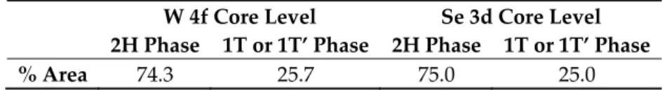
The WSe2 nanosheets were investigated by X‐ray photoelectron spectroscopy (XPS). The XPS
spectra recorded on the W 4f and Se 3d binding energy regions are shown in Figure 7. Considering the W 4f spectrum (Figure 7a), the following three main peaks can be observed: two main contributions at about 32.5 and 34.6 eV are attributed to the doublets W 4f7/2 and W 4f5/2, respectively, and a wide and low intense contribution of around 37.8 eV is attributed to the W 5p3/2. The main contribution can be fitted with two doublets centered at 31.9 and 32.5 eV on a W 4f7/2 signal, attributed to the 1T’ [34] or 1T [35] phase and 2H phase, respectively. The 2H contribution (centered at 32.5 eV) corresponds to 75.0% of the total area, indicating that the sample mainly has a 2H phase. Another additional smaller contribution is observed at 35.5 eV, due to the W 4f loss. Figure 7. XPS spectra of the (a) W 4f and (b) Se 3d of the WSe2 nanosheets. The formation of two phases is further confirmed on the Se 3d core level spectra (Figure 7b). The
spectrum shows the presence of two main peaks, Se 3d5/2 and Se 3d3/2 doublets, at around 54.8 and
55.6 eV, respectively. Each doublet can be fitted with two components—one at 54.8 eV, corresponding
to the 2H‐WSe2 phase, and one corresponding to the other phase (1T or 1T’), centered at 54.3 eV. Here,
again, the 2H phase represents nearly 75% of the total area (Table 1), verifying the conclusions
crystals [34,35], with a major 2H phase and a minor other phase assigned to the 1T’ [34] or 1T [35] phases, respectively.
Table 1. Percentages of the corresponding areas of different phases of WSe2 nanosheets.
W 4f Core Level Se 3d Core Level
2H Phase 1T or 1T’ Phase 2H Phase 1T or 1T’ Phase
% Area 74.3 25.7 75.0 25.0
Information about the phases and the quantitative proportion between the phases can be obtained using high resolution XPS spectra, with an energy shift of around 0.8–1 eV in binding energy for the 2H phase compared with the 1T phase, in the two regions of interest, W4f and Se3d [35], and
as reported for MoS2 [36]. However, if the distinction between the 2H phase and the 1T phase can be
done by XPS, the type of 1T phase—1T or distorted 1T, called 1T’—cannot be elucidated by this technique (only by advanced electron microscopy techniques).
Based on these XPS results, the presence of two phases has been demonstrated in the WSe2 synthesized material.
We must note that Raman spectroscopy can be also a powerful tool to differentiate the number
of layers and phases. The MoS2 material can be given in the example where the frequency difference
of the two modes, E2g1 and A1g, is a function of the layer thickness [37], and the apparition of additional weak modes, J1, J2, and J3, with a decreasing of E2g1 peak intensity for the 1T phase [36,38]. Concerning
the WSe2 material, the Raman spectrum of the 1T’ WSe2 phase clearly shows a distinct number of
weak peaks, which are reminiscent of these J modes [34]. In our studies, however, the contribution of the 2H phase in the Raman signature is overriding, explaining the shape of the spectrum with the high intensity of E2g1. Concerning the results obtained by the photoluminescence and optical absorption spectroscopy, the 1T phases do not produce characteristic features, because of their metallic properties [34,39], and the spectra shape in both cases comes from the semiconducting 2H phase. The last comment concerns the XRD results, where the experimental identification of the different phases is also difficult, because of the similar lattice constants and symmetries.
4. Conclusions
The synthesis of the WSe2 film was achieved using an atmospheric pressure CVD technique. We
have shown that the synthesized film is constituted of highly crystalline vertically aligned nanosheets. The presence of another phase different to the 2H stable phase has been shown, and could open a new route to tune the physical properties by phase engineering, as has already been
done for similar materials, such as MoTe2. The underlying growth mechanism must be further
studied in order to establish the best parameters so as to control the synthesis of the WSe2 film with different phases. Further studies will be performed aiming at the evaluation of this material active layer in different applications, such as gas sensing and hydrogen evolution reaction catalysis. Supplementary Materials: The following are available online at www.mdpi.com/xxx/s1, Figure S1: Scheme of WSe2 synthesis. Author Contributions: A.S.‐C. and J.‐F.C. conceived, and carried out the experiments. S.A. and C.B. contributed to the Raman and PL measurements. E.H. contributed to XPS measurements and analysis. A.S.‐C. and J.‐F.C. made the analysis of the data. A.S.‐C. and J.‐F.C. wrote the manuscript. All of the authors provided critical feedback and helped shape the research and analysis. All authors have read and agreed to the published version of the manuscript.
Funding: This research work was financed by a grant from the University of Namur, Belgium. J.‐F.C. and C.B.
are Senior Research Associates and Research Associates of FRS‐FNRS (Belgium), respectively.
Acknowledgments: The Synthesis, Irradiation, and Analysis of Materials (SIAM), PC2, and MORPH‐IM
Appl. Sci. 2020, 10, 874 8 of 9 Conflicts of Interest: The authors declare no conflict of interest. The funders had no role in the design of the study; in the collection, analyses, or interpretation of data; in the writing of the manuscript; or in the decision to publish the results. References 1. Chhowalla, M.; Shin, H.S.; Eda, G.; Li, L.J.; Loh, K.P.; Zhang, H. The chemistry of two‐dimensional layered transition metal dichalcogenide nanosheets. Nat. Chem. 2013, 5, 263. 2. Hao, G.; Kou, L.; Lu, D.; Peng, J.; Li, J.; Tang, C.; Zhong, J. Electrostatic properties of two‐dimensional WSe2 nanostructures. J. Appl. Phys. 2016, 119, 035301. 3. Chiritescu, C.; Cahill, D.G; Nguyen, N.; Johnson, D.; Bodapati, A.; Keblinski, P.; Zschack, P. Ultralow termal conductivity in disordered, layered WSe2 crystals. Science 2007, 315, 351–353. 4. Velazquez, J.M.; Saadi, F.H.; Pieterick, A.P.; Spurgeon, J.M.; Soriaga, M.P.; Brunschwig, B.S.; Lewis, N.S. Synthesis and hydrogen‐evolution activity of tungsten selenide thin films deposited on tungsten foils. J. Electroanal. Chem. 2014, 716, 45–48.
5. Wang, H.; Kong, D.; Johanes, P.; Cha, J.; Zheng, G.; Yan, K.; Liu, N.; Cui, Y. MoS2 and WSe2 nanofilms with
vertically aligned moleculer layers on curved and rough surfaces. ACS Nano 2013, 13, 3426–3433.
6. Bozheyev, F.; Friedrich, D.; Nie, M.; Rengachari, M.; Ellmer, K. Preparation of highly (001)‐oriented photoactive tungstene diselenide (WSe2) by an amorphous solid‐liquid‐crystalline solid (aSLcS) rapid‐
crystallization process. Phys. Status Solidi A 2014, 211, 2013–2019.
7. Jana, M.J.; Rao, C.N.R. Two dimensional analogues of graphene: Transition metal dichalgenides. Phil. Trans. R. Soc. A 2016, 374, 20150318.
8. Fang, H.; Chuang, S.; Chang, T.C.; Takei, K.; Takahashi, T.; Javey, A. High‐performance single layered WSe2
p‐FETs with chemically doped contacts. Nano Lett. 2012, 12, 3788–3792.
9. Baugher, B.W.H.; Churchill, H.O.H.; Yang, Y.; Jarillo‐Herrero, P. Optoelectronic devices based on
ellectrically tunable p‐n diodes in a monolayer dichalcogenide. Nat. Nanotechnol. 2014, 9, 262–267.
10. Ross, J.S.; Klement, P.; Jones, A.M.; Ghimire, N.J.; Yan, J.; Mandrus, D.G.; Taniguchi, T.; Watanabe, K.;
Kitamura, K.; Yao, W.; et al. Electrically tunable excitonic light‐emitting diodes based on monolayer WSe2 p‐n junctions. Nat. Nanotechnol. 2014, 9, 268–272. 11. Pospischil, A.; Furchi, M.M.; Mueller, T. Solar‐energy conversion and light emission in a atomic monolayer p‐n diodes. Nat. Nanotechnol. 2014, 9, 257–261. 12. Jäger‐Waldau, A.; Bucher, E. WSe2 thin films prepared by soft selenization. Thin Solid Films 1991, 200, 157– 164.
13. Patel, A.A.; Rathod, J.R.; Patel, H.S.; Patel, K.D.; Pathak, V.M. Structural and optical characterization of tungstene diselenide crystals grown by DVT technique. Adv. Mater. Res. 2013, 665, 53–57.
14. Li, H.; Gao, D.; Li, K.; Pang, M.; Xie, S.; Liu, R.; Zou, J. Texture control and growth mechanism of WSe2 film
prepared by rapid selenization of W film. Appl. Surf. Sci. 2017, 394, 142–148.
15. Li, H.; Lu, G.; Wang, Y.; Yin, Z.; Cong, C.; He, Q.; Wang, L.; Ding, F.; Yu, T.; Zhang, H. Mechanical exfoliation and characterization of single and few‐layer nanosheets of WSe2, TaS2 and TaSe2. Small 2013, 9,
1974–1981.
16. Magda, G.Z.; Peto, J.; Dobrik, G.; Hwang, C.; Biró, L.P.; Tapasztó, L. Exfoliation of large‐area metal chalcogenide single layers. Sci. Rep. 2015, 5, 14714.
17. Wang, Y.; Zhao, S.; Wang, Y.; Laleyan, D.A.; Wu, Y.; Ouyang, B.; Ou, P.; Song, J.; Mi, Z. Wafer‐scale
synthesis of monolayer WSe2: A multi‐functional photocatalyst for efficient overall pure water splitting. Nano Energy 2018, 51, 54–60. 18. Grigoriev, S.N.; Fominski, V.Y.; Gnedovets, A.G.; Romanov, R.I. Experimental and numerical study of the chemical composition of WSex thin films obtained by pulsed laser deposition in vacuum and in a buffer gas atmosphere. Appl. Surf. Sci. 2012, 258, 7000–7007. 19. Zhang, B.‐Q.; Chen, J.‐S.; Niu, H.‐L.; Mao, C.‐J.; Song, J.‐M. Synthesis of ultrathin WSe2 nanosheets and their high‐performance catalysis for conversion of amines to imines. Nanoscale 2018, 10, 20266–20271. 20. Jung, W.; Lee, S.; Yoo, D.; Jeong, D.; Miro, P.; Kuc, A.; Heine, T.; Cheon, J. Colloidal synthesis of single‐ layer MSe2 (M = Mo, W) nanosheets via anisotropic solution‐phase growth approach. J. Am. Chem. Soc. 2015, 137, 7266–7269.
21. Jebaraj Devadasan, J.; Sanjeviraja, C.; Jayachandran, M. Electrosynthesis and characterization of n‐WSe2
22. Huang, J.K.; Pu, J.; Hsu, C.L.; Chiu, M.H.; Juang, Z.Y.; Chang, Y.H.; Chang, W.H.; Iwasa, Y.; Takenobu, T.;
Li, L.J. Large‐area synthesis of highly crystalline WSe2 monolayers and device applications. ACS Nano 2013,
8, 923–930.
23. Boscher, N.D.; Carmalt, C.J.; Parkin, I.P. Atmospheric pressure chemical vapor deposition of WSe2 thin
films on glass‐highly hydrophobic sticky surfaces. J. Mater. Chem. 2006, 16, 122–127. 24. Liu, B.; Fathi, M.; Chen, L.; Abbas, A.; Ma, Y.; Zhou, C. Chemical vapor deposition growth of monolayer WSe2 with tunable device characteristics and growth mechanism study. ACS Nano 2015, 9, 6119–6127. 25. Chen, J.; Liu, B.; Liu, Y.; Tang, W.; Chang, C.T.; Li, L.; Zheng, J.; Gao, L.; Zheng, Y.; Shin, H.S.; et al. Chemical vapor deposition of large‐sized hexagonal WSe2 crystals on dielectric substrates. Adv. Mater. 2015, 27, 6722– 6727.
26. Liu, J.; Zeng, M.; Wang, L.; Chen, Y.; Xing, Z.; Zhang, T.; Liu, Z.; Zuo, J.; Nan, F.; Mendes, R.G.; et al. Ultrafast self‐limited growth of strictly monolayer WSe2 crystals. Small 2016, 12, 5741–5749.
27. Chen, L.; Liu, B.; Abbas, A.N.; Ma, Y.; Fang, X.; Liu, Y.; Zhou, C. Screw‐dislocation‐driven growth of two‐
dimensional few‐layer and pyramid‐like WSe2 by sulfur‐assisted chemical vapor deposition. ACS Nano
2014, 8, 11543–11551.
28. Deokar, G.; Vignaud, D.; Arenal, R.; Louette, P.; Colomer, J.F. Synthesis and characterization of MoS2
nanosheets. Nanotechnology 2016, 27, 075604.
29. Salitra, G.; Hodes, G.; Klein, E.; Tenne, R. Highly oriented WSe2 thin films prepared by selenization of
evaporated WO3. Thin Solid Film. 1994, 245, 180–185.
30. Tonndorf, P.; Schmidt, R.; Böttger, P.; Zhang, X.; Börner, J.; Liebig, A.; Albrecht, M.; Kloc, C.; Gordan, O.;
Zahn, D.R.T.; et al. Photoluminescenc emission and Raman response of monolayer MoS2, MoSe2 and WSe2.
Opt. Express 2013, 21, 1908–4916.
31. Li, Y.; Li, X.; Yu, T.; Yang, G.; Chen, H.; Zhang, C.; Feng, Q.; Ma, J.; Liu, W.; Xu, H.; et al. Accurate
identification of layer number for few‐layer WS2 and WSe2 via spectroscopic study. Nanotechnology 2018,
29, 124001.
32. Zhao, W.; Ghorannevis, Z.; Chu, L.; Toh, M.; Kloc, C.; Tan, P.H.; Eda, G. Evolution of electronic structure in atomically thin sheets of WS2 and WSe2. ACS Nano 2012, 7, 791–797.
33. Beal, A.R.; Knights, J.C.; Liang, W.Y. Transmission spectra of some transition metal dichalcogenides. II. Group VIA: Trigonal prismatic coordination. J. Phys. C Solid State Phys. 1972, 5, 3540.
34. Sokolikova, M.S.; Sherrell, P.C.; Palczynski, P.; Bemmer, V.L.; Mattevi, C. Direct solution‐phase synthesis of 1T’ WSe2 nanosheets. Nat. Commun. 2019, 10, 712.
35. Wu, P.C.; Yang, C.L.; Du, Y.; Lai, C.H. Scalable epitaxial growth of WSe2 thin films pn SiO2/Si vai a self‐
assembled PtSe2 buffer layer. Sci. Rep. 2019, 9, 8017. 36. Eda, G.; Yamaguchi, H.; Voiry, D.; Fujita, T.; Chen, M.; Chhowalla, M. Photoluminescence from chemically exfoliated MoS2. Nano Lett. 2011, 11, 5111–5116. 37. Calandra, M. Chemically exfoliated single‐layer MoS2: Stability, lattice dynamics, and catalytic adsorption from first principles. Phys. Rev. B 2013, 88, 245428. 38. Lee, C.; Yan, H.; Brus, L.E.; Heinz, T.F.; Hone, J.; Ryu, S. Anomalous lattice vibrations of single‐ and few‐ layers MoS2. ACS Nano 2010, 4, 2695–2700. 39. Ma, Y.; Liu, B.; Zhang, A.; Chen, L.; Fathi, M.; Shen, C.; Abbas, A.N.; Ge, M.; Mecklenburg, M.; Zhou, C. Reversible semiconducting‐to‐metallic phase transition in chemical vapor deposition grown monolayer WSe2 and applications for devices. ACS Nano 2015, 9, 7383–7391. © 2020 by the authors. Licensee MDPI, Basel, Switzerland. This article is an open access article distributed under the terms and conditions of the Creative Commons Attribution (CC BY) license (http://creativecommons.org/licenses/by/4.0/).