HAL Id: hal-01745840
https://hal.archives-ouvertes.fr/hal-01745840
Submitted on 16 Jul 2018HAL is a multi-disciplinary open access
archive for the deposit and dissemination of sci-entific research documents, whether they are pub-lished or not. The documents may come from teaching and research institutions in France or abroad, or from public or private research centers.
L’archive ouverte pluridisciplinaire HAL, est destinée au dépôt et à la diffusion de documents scientifiques de niveau recherche, publiés ou non, émanant des établissements d’enseignement et de recherche français ou étrangers, des laboratoires publics ou privés.
Quantum Simulation of C-V and I-V Characteristics in
Ge and III-V Materials/High-κ MOS Devices
Mathieu Moreau, Daniela Munteanu, Jean-Luc Autran, Florence Bellenger,
Jérome Mitard, Michel Houssa
To cite this version:
Mathieu Moreau, Daniela Munteanu, Jean-Luc Autran, Florence Bellenger, Jérome Mitard, et al.. Quantum Simulation of C-V and I-V Characteristics in Ge and III-V Materials/High-κ MOS Devices. MRS Online Proceedings Library, 2009, 1194, pp.1194-A02-02. �10.1557/PROC-1194-A02-02�. �hal-01745840�
Quantum Simulation of C-V and I-V Characteristics in Ge and III-V Materials/High-κ MOS Devices
Mathieu Moreau1, Daniela Munteanu1, Jean-Luc Autran1, Florence Bellenger2,3, Jérôme Mitard2, and Michel Houssa2,3
1
IM2NP-CNRS (UMR 6242), Bât. IRPHE, 49 rue Joliot Curie, BP 146, F-13384 Marseille Cedex 13, France
2
IMEC, Kapeldreef 75, B-3001 Leuven, Belgium
3
K.U. Leuven, Celestijnenlaan 200d, B-3001 Leuven, Belgium
ABSTRACT
We present a one-dimensional simulation study of the capacitance-voltage (C-V) and current-voltage (I-V) characteristics in MOS devices with high mobility semiconductors (Ge and III-V materials) and non-conventional gate stack with high-κ dielectrics. The C-V quantum simulation code self-consistently solves the Schrödinger and Poisson equations and the electron transport through the gate stack is computed using the non-equilibrium Green’s function formalism (NEGF). Simulated C-V characteristics are successfully confronted to experimental data for various MOS structures with different semiconductors and dielectric stacks. Simulation of I-V characteristics reveals that gate leakage current strongly depends on gate stacks and substrate materials and predicts low leakage current for future CMOS devices with high mobility materials and high-κ dielectrics.
INTRODUCTION
In order to improve complementary metal-oxide-semiconductor (CMOS) technology performances for future technological nodes (sub 22-16 nm), high mobility (high-µ)
semiconductors with high permittivity (high-κ) dielectric-based gate stacks have been recently considered to replace the historical SiO2/Si structure [1].
Due to low values of the carrier conductivity effective masses in both valence and conduction bands, which leads to higher hole and electron mobilities than in Si, Ge and III-V materials are seriously considered in recent works to respectively enhance p-MOSFET and n-MOSFET performances, especially the on-state current in high-performance logic applications. Moreover, the introduction of high-κ dielectrics can reduce tunneling current through the gate stack while maintaining control of the current in the channel by the gate even for structures with very low equivalent oxide thickness (EOT) [2].
However, the fabrication of high-κ/Ge (or III-V) devices in terms of surface passivation between gate oxide and channel material is still not well controlled and remains a challenge to meet ITRS roadmap requirements. Over the past few years, countless techniques and materials have been used to manufacture devices (GeO2 [3-5], La2O3 [6], Ga2O3(Gd2O3) [7], Al2O3 [8],
HfO2/SiO2/Si [9], HfO2 [10]); all these technologies lead to complicated structures with multi
layer gate stacks, for which it is difficult to precisely extract key parameters and predict future performances.
In this context, we present a one-dimensional (1D) simulation study of capacitance-voltage and current-voltage characteristics in MOS devices with high-µ channel materials and multi layer high-κ gate stacks. We self-consistently solve Poisson and Schrödinger equations to compute the
quantum carrier density and we use it to calculate the capacitance and the gate leakage current as a function of the applied gate voltage.
THEORETICAL DETAILS
The simulation code is based on the 1D self-consistent numerical solving of the Poisson and Schrödinger equations coupled with the computation of the high/low frequency capacitance and the calculation of the gate current in MOS devices.
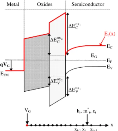
In order to calculate the “quantum” carrier (electrons and holes) densities, we have to solve the time-independent, effective mass 1D Schrödinger equation. The numerical solution of this equation is obtained by using the three-point finite-difference scheme applied to a non-uniform mesh along x-axis (figure 1) [11,12]. The total quantum electron and hole densities (2D gas) are obtained as in [11] and used to solve the 1D Poisson equation with a material-dependent
dielectric constant (εi) along the grid.
Once the Schrödinger-Poisson system is solved, the resulting quantum carrier density in the substrate is used for calculating the low and high-frequency capacitance of the structure [12]. The gate current density is evaluated from the 2D carrier gas in the inversion regime using the formalism presented in [13,14], where the carrier transmission probability is calculated with the Wentzel-Kramers-Brillouin (WKB) classical approximation.
x xi xi+1 xi-1 hi, m * i, εi VG qVG Ec(x) EFM EF EV EC EG
Metal Oxides Semiconductor
1 ox C E ∆ 2 ox C E ∆ 2 ox V E ∆ 1 ox V E ∆
However, quantum-mechanical effects markedly affect the transport of carrier and the WKB approximation is not able to perfectly describe quantum reflections against abrupt electrical potential variations as it is the case in MOS devices with multi layer gate stacks [15]. Thus, we have also computed the gate current using a full quantum-mechanical approach, namely the non-equilibrium Green’s function (NEGF) formalism [16]. This method solves the Schrödinger equation with open boundary conditions, taking into account both wave-function reflections and attenuations on the potential barrier (figure 1), and was adapted for metal-insulator-metal (MIM) structures [15,17] with an effective-mass depending on the position along a 1D grid in the transport direction.
The main material parameters used in simulations are presented in Table I. It is important to note that these constants (dielectric constant, effective mass…) strongly depend on the
fabrication process and are not exactly known, especially for dielectric materials. Thus, the values in the simulation code can be adapted in order to improve the fit between experimental and simulation results.
Figure 1. Schematic band diagram of a MOS structure (p-type
semiconductor) for VG > 0 and the main physical parameters
used in the simulation (listed in Table I). The discretization of the 1D structure using a uniform mesh in oxides and non-uniform mesh in semiconductor is also represented.
Table I. Main material parameters [3,18,19] of different semiconductors and dielectric materials
used for MOS device simulation. The band offsets between oxides and semiconductors (not shown here) are the same as in reference [20] except for Ge/GeO2 interface [18].
EG (V) ε/ε0 m*e,l/m0 (gl) m * e,t/m0 (gt) m * lh/m0 m * hh/m0 m * so/m0 Si 1.12 11.8 0.916 (2) 0.19 (4) 0.20 0.291 0.29 Ge 0.66 16.0 0.044 0.28 0.084 GaAs 1.424 10.9 0.082 0.51 0.15 GaSb 0.726 14.4 0.050 0.40 0.14 InP 1.34 9.61 0.089 0.60 0.17 InAs 0.354 12.3 0.026 0.41 0.16 InSb 0.17 15.7 0.015 0.43 0.19 SiO2 9.0 3.9 GeO2 4.3 6.7 Al2O3 6.1 9.0 HfO2 5.6 20.0 0.17 0.35 0.949 (4)
Materials Physical Parameters (300 K)
0.063 (1) 0.041 (1) 0.014 (1) 0.5 0.5 0.080 (1) 0.014 (1)
RESULTS AND DISCUSSION
We first illustrate C-V characteristics by comparing, in figure 2, our simulated results and experimental data [3] for high-frequency curves in two different double-layer gate stacks with a p-doped Ge substrate. Simulated and experimental data are in good agreement in depletion and accumulation regimes, which show the possibility to use the simulated curves to extract oxide material parameters such as dielectric constant, interfacial layer physical thickness and flat-band voltage [12]. 0 0,005 0,01 0,015 0,02 -2 -1 0 1 2 C a p a ci ta n ce ( F /m 2) Gate Voltage VG(V) experiment [3] simulation
HfO2/GeO2/p-Ge
Al2O3/GeO2/p-Ge 1 MHz 0.020 0.015 0.010 0.005 0 0 0,005 0,01 0,015 0,02 0,025 0,03 -2 -1 0 1 C a p a ci ta n ce ( F /m 2) Gate Voltage VG(V) GaSb InSb InAs GaAs InP 0.030 0.025 0.020 0.015 0.010 0.005 0 EOT = 1.0 nm NA= 1017cm-3 ΦM= 5 eV
Figure 2. Comparison between experimental
data [3] (symbol) and simulated (line) C-V curves for HfO2/GeO2/p-Ge (black, ΦM =
4.83 eV) and Al2O3/GeO2/p-Ge (red, ΦM =
4.50 eV) MOS structures (NA = 1017 cm-3,
THfO2 = TAl2O3 = 4.0 nm, TGeO2 = 1.4 nm).
Figure 3. Simulated C-V characteristics for
five different III-V p-doped semiconductors (NA = 1017 cm-3) with an Al2O3 gate
dielectric layer of 2.3 nm (EOT = 1.0 nm) and ΦM = 5 eV (fixed for all structures).
We have also adapted our simulation code to calculate C-V characteristics for different III-V semiconductors. Figure 3 compares simulation results for various Al2O3/III-V materials MOS
devices (TAl2O3 = 2.3 nm, i.e. EOT = 1.0 nm) for which the gate work function is equal to 5 eV
for all structures. We can see in this figure that the depletion zone strongly depends on the semiconductor bandgap, i.e. smaller is the bandgap and shorter is the depletion zone thickness (in terms of gate voltage). Moreover, the very low effective density of state in the conduction band of III-V semiconductors is clearly evidenced in inversion regime, which leads to low capacitance values in C-V characteristics.
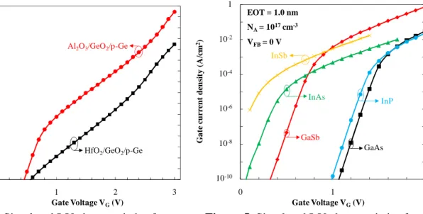
Figures 4 and 5 show the I-V curves of the structures related to figures 2 and 3, respectively. The gate current curves in double-layer gate stacks with Ge substrate (figure 4) show very low values principally due to a large physical thickness of high-κ layer (HfO2 and Al2O3), which
strongly reduces the tunneling current. The gate current in experimental devices (not shown here) seems to be higher probably due to different additional conduction mechanisms, such as trap-assisted conduction in the high-κ layer (which is not taken into account in our simulation code). However, we observe that the conduction band offset between the two oxide layers is one of the main parameters influencing the gate leakage tunneling current. Indeed, the conduction band offset between Al2O3 and GeO2 is higher than the case between HfO2 and GeO2 [18], which
leads to higher gate current for Al2O3/GeO2 structure. We also show in figure 5 (the gate current
of structures of figure 3 is plotted) that the substrate material is also crucial to reduce the gate current. In other words, semiconductors with very low bandgap (InAs or InSb) give high currents (besides we do not take into account band-to-band tunneling, which will additionally increase the current) whereas GaAs and InP seems to be very promising substrate materials in terms of low leakage current. 1,E-10 1,E-09 1,E-08 1,E-07 1,E-06 1,E-05 1,E-04 1,E-03 1,E-02 1,E-01 1,E+00 1,E+01 1,E+02 1,E+03 1,E+04 1,E+05 1,E+06 0 1 2 3 G a te cu rr en t d en si ty ( A /c m 2) Gate Voltage VG(V) HfO2/GeO2/p-Ge
Al2O3/GeO2/p-Ge 102 1 10-2 10-4 10-6 10-8 10-10 10-12 10-14 1,E-10 1,E-09 1,E-08 1,E-07 1,E-06 1,E-05 1,E-04 1,E-03 1,E-02 1,E-01 1,E+00 0 1 2 G a te c u rr en t d en si ty ( A /c m 2) Gate Voltage VG(V) GaSb InAs GaAs InP InSb 1 10-2 10-4 10-6 10-8 10-10 EOT = 1.0 nm NA= 1017cm-3 VFB= 0 V
Figure 4. Simulated I-V characteristics for
the same devices as figure 2.
Figure 5. Simulated I-V characteristics for the
same devices as figure 3. In this figure, VFB is
fixed at 0 V for all structures.
In order to study the influence of oxide material parameters, we now present results concerning MIM capacitors using a full quantum-mechanical calculation (NEGF formalism). Figure 6 compares the tunneling transmission probability through the gate stack between NEGF and WKB calculations for a double-layer gate stack [SiO2 (6 Å) + HfO2 (20.5 Å)]. We can
observe that classical (WKB) and quantum (NEGF) calculation lead to significant differences between the two transmission curves due to strong potential discontinuities (metal/insulator and insulator/insulator band offset) [16]. The quantum reflections are clearly revealed when the energy-resolved LDOS is plotted (insert of figure 6). The LDOS structure presents a subband energy splitting similar to those corresponding to a quantum well, formed by the barrier
discontinuities at the insulator boundaries. The peaks in the transmission probability correspond to a resonant tunneling condition due to a reinforced DOS at the considered energy levels [16,17].
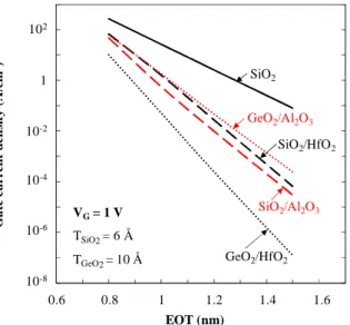
We finally plot, in figure 7, the evolution of gate current density as a function of EOT for different MIM structures at VG = 1 V. From these results, we clearly see that the gate current
depends on several parameters such as oxide band offsets or dielectric constants. The best way to reduce the leakage current seems to be using dielectric materials with a high permittivity value and a very low band offset between the high-κ and interfacial layers. One can also observe that simulated double-layer gate stacks always give better results than the single SiO2 layer.
1,E-07 1,E-06 1,E-05 1,E-04 1,E-03 1,E-02 1,E-01 1,E+00 0 1 2 3 4 T ra n sm is si o n p ro b a b il it y Energy (eV) 1 10-1 10-2 10-3 10-4 10-5 10-6 10-7 WKB NEGF EOT = 1 nm VG= 1 V 1,E-08 1,E-07 1,E-06 1,E-05 1,E-04 1,E-03 1,E-02 1,E-01 1,E+00 1,E+01 1,E+02 1,E+03 0,6 0,8 1 1,2 1,4 1,6 G a te c u rr en t d en si ty ( A /c m 2) EOT (nm) SiO2/HfO2 102 1 10-2 10-4 10-6 10-8 SiO2 VG= 1 V TSiO2= 6 Å TGeO2= 10 Å GeO2/Al2O3 SiO2/Al2O3 GeO2/HfO2 0.6 0.8 1 1.2 1.4 1.6
Figure 6. Carrier transmission probability
calculated using WKB and NEGF formalisms as a function of energy in MIM capacitor with a double-layer gate stack SiO2 (6 Å) +
HfO2 (20.5 Å). The insert show
energy-resolved LDOS and energy band diagram.
Figure 7. Calculation of gate current density
(NEGF formalism) vs EOT for different MIM devices [SiO2, SiO2 or GeO2 + HfO2
(long dash), SiO2 or GeO2 + Al2O3 (short
dash)] with TSiO2 = 6 Å or TGeO2 = 10 Å in
double-layer gate stacks at VG = 1 V.
CONCLUSION
We developed a 1D numerical simulation code for the calculation of the C-V and I-V characteristics of MOS devices with high-µ materials and high-κ gate stack. The code self-consistently solves the Schrödinger and Poisson equations and the resulting quantum carrier density in the substrate is used to calculate the capacitance of the structure. The electron transport through the gate stack is treated using the NEGF formalism. Comparison with C-V experimental data shows that the code can be used to extract the value of key parameters in MOS structures with arbitrary multi layer high-κ gate stacks. Simulation of I-V characteristics reveals
-1 0 1 2 3 4 0 0,5 1 1,5 2 2,5 3 E n er g y ( eV ) x (nm) HfO2 SiO2
that gate leakage current strongly depends on gate stacks and substrate materials. These results also predict promising performances in terms of low leakage current confirming the possibility of enhancing CMOS performances with high-µ materials and high-κ gate stacks.
ACKNOWLEDGMENTS
This work was supported by the CNRS International Project of Scientific Collaboration (PICS) between IM2NP, Marseille, France and IMEC, Leuven, Belgium.
REFERENCES
1. S. E. Laux, IEEE Trans. Electron Dev. 54, 2304 (2007).
2. M. Houssa and M. M. Heyns, in High-κ Gate Dielectrics, edited by M. Houssa (IOP Publishing, Bristol, U. K., 2004), Chap. 1.1.
3. A. Delabie, F. Bellenger, M. Houssa, T. Conard, S. Van Elshocht, M. Caymax, M. Heyns, and M. Meuris, Appl. Phys. Lett. 91, 082904 (2007).
4. R. Xie, T. H. Phung, W. He, Z. Sun, M. Yu, Z. Cheng, and C. Zhu, IEDM 08 Proceedings, 393 (2008).
5. Y. Nakakita, R. Nakane, T. Sasada, H. Matsubara, M. Takaneka, and S. Takagi, IEDM 08
Proceedings, 877 (2008).
6. C. Andersson, M. Sousa, C. M. Marchiori, D. J. Webb, D. Caimi, H. Siegwart, J.
Fompeyrine, C. Rossel, A. Dimoulas, and Y. Panayiotatos, ESSDERC 09 Proceedings, 179 (2009).
7. T. D. Lin, H. C. Chiu, P. Chang, Y. H. Chang, C. A. Lin, W. H. Chang, J. Kwo, W. Tsai, and M. Hong, ESSDERC 09 proceedings, 399 (2009).
8. Y. Xuan, Y. Q. Wu, and P. D. Ye, IEEE Electron Devices Lett. 29, 294 (2008). 9. J. Mitard et al., IEDM 08 Proceedings, 873 (2008).
10. W. P. Bai, N. Lu, A. Ritenour, M. L. Lee, D. A. Antoniadis, and D.-L. Kwong, IEEE
Electron Devices Lett. 27, 175 (2006).
11. C. Raynaud, J.-L. Autran, P. Masson, M. Bidaud, and A. Poncet in Structure and Electronic
Properties of Ultrathin Dielectric Films on Silicon and Related Structures, edited by H.J.
von Bardeleben, A.H. Edwards, T. Hattori, and D.A. Buchanan, (Mater. Res. Soc. Symp. Proc. 592, Warrendale, PA, 2000) 190.
12. M. Moreau, D. Munteanu, J. L. Autran, F. Bellenger, J. Mitard, and M. Houssa, J.
Non-Cryst. Solids 355, 1171 (2009).
13. F. Li, S. P. Mudanai, Y.-Y. Fan, L. F. Register, and S. K. Banerjee, IEEE Trans. Electron
Dev. 53, 1096 (2006).
14. W.Wang, N. Gu, J. P. Sun, P. Mazumder, Solid-State Electron. 50, 1489 (2006). 15. M. Moreau, D. Munteanu, and J. L. Autran, Jpn. J. Appl. Phys. 48, (2009) (in press). 16. S. Datta, Superlattices Microstruct. 28, 253 (2000).
17. D. Munteanu, J. L. Autran, M. Moreau, and M. Houssa, J. Non-Cryst. Solids 355, 1180 (2009).
18. V. V. Afanas’ev, A. Stesmans, A. Delabie, F. Bellenger, M. Houssa, and M. Meuris, Appl.
Phys. Lett. 92, 022109 (2008).
19. http://www.ioffe.rssi.ru/SVA/NSM/
![Figure 2. Comparison between experimental data [3] (symbol) and simulated (line) C-V curves for HfO 2 /GeO 2 /p-Ge (black, Φ M = 4.83 eV) and Al 2 O 3 /GeO 2 /p-Ge (red, Φ M = 4.50 eV) MOS structures (N A = 10 17 cm -3 , T HfO2 = T Al2O3 = 4.0 n](https://thumb-eu.123doks.com/thumbv2/123doknet/14663774.740233/4.892.456.777.664.954/figure-comparison-experimental-symbol-simulated-curves-black-structures.webp)