HAL Id: hal-01694202
https://hal.archives-ouvertes.fr/hal-01694202
Submitted on 9 May 2018
HAL is a multi-disciplinary open access
archive for the deposit and dissemination of
sci-entific research documents, whether they are
pub-lished or not. The documents may come from
teaching and research institutions in France or
abroad, or from public or private research centers.
L’archive ouverte pluridisciplinaire HAL, est
destinée au dépôt et à la diffusion de documents
scientifiques de niveau recherche, publiés ou non,
émanant des établissements d’enseignement et de
recherche français ou étrangers, des laboratoires
publics ou privés.
Strain-induced electronic band convergence: effect on
the Seebeck coefficient of Mg2Si for thermoelectric
applications
H. Balout, P. Boulet, M. -C. Record
To cite this version:
H. Balout, P. Boulet, M. -C. Record. Strain-induced electronic band convergence: effect on the Seebeck
coefficient of Mg2Si for thermoelectric applications. Journal of Molecular Modeling, Springer Verlag
(Germany), 2017, 23 (4), pp.130 - 130. �10.1007/s00894-017-3304-1�. �hal-01694202�
(will be inserted by the editor)
Strain-induced electronic band convergence: effect on the Seebeck
coefficient of Mg
2Si for thermoelectric applications
H. Balout · P. Boulet · M.-C. Record
Received: date / Accepted: date
Abstract The present theoretical study, performed using density-functional theory and Boltzmann transport theory formalisms, shows that, under 2.246% isotropic tensile strain, the two energy-lowest conduction bands of Mg2Si overlap. The two, threefold degenerated orbitals become a unique, sixfold degenerated orbital. It is
demonstrated that, such degeneracy implies an increase of the Seebeck coefficient, of the electrical conductiv-ity, of the power factor, and in fine of the figure of merit.
Keywords Thermoelectricity · isotropic constraints · silicides · band structures · Density-functional theory · Boltzmann transport theory
H. Balout
MADIREL, Aix-Marseille University and CNRS, Avenue Normandie-Niemen, 13397 Marseille cedex 20, France
Present address: Institut de Physique Nucléaire, Université Paris-Sud 11 and CNRS, 15 rue Georges Clémenceau, 91406 Orsay, France
P. Boulet
MADIREL, Aix-Marseille University and CNRS, Avenue Normandie-Niemen, 13397 Marseille cedex 20, France, E-mail: [email protected]
M.-C. Record
1 Introduction
The rarefaction of fossil fuels and their environmental impact have made the concerns about energy grown fast over the past decades. New ways of energy production, such as batteries, photovoltaic and thermoelectricity, are intensively explored. The principles of thermoelectricity are based on the direct conversion between elec-trical and thermal energies [1]. The performance of a thermoelectric material is measured by three parameters, namely the Seebeck coefficient S, the electrical conductivity σ and the thermal conductivity κ; these parameters are connected by a dimensionless factor, the so-called figure of merit zT , with zT = T S2
σ /κ , where T is the absolute temperature [2]. According to this equation, it appears that a way to reach high zT is that the material shows a large Seebeck coefficient, a good electrical conductivity and, at the same time, a low thermal conduc-tivity. However the improvement of the heat-to-electricity conversion by materials is made difficult due to the inverse relationships between the electronic thermal conductivity and the electrical conductivity (Wiedemann-Franz law) and between the Seebeck coefficient and the electrical conductivity (Boltzmann’s transport theory). Hence, the best materials found so far result from the best compromise between the transport properties.
The improvement of the power factor S2σ , and hence of zT , could be obtained by separately controling the electrical conductivity and the Seebeck coefficient, which can be achieved by band structure engineering. Band engineering consists in electronic band manipulations so as to create density of states (DOS) resonant levels [3] or electronic band degeneracy (see for instance [4–7]). The DOS effective mass is then increased which in turn increases the Seebeck coefficient of the material [3, 8, 9].
Chasmar and Stratton [10] showed that, when assuming that in doped materials the dopants only affect the chemical potential level, the best figure of merit value can be achieved by increasing the β quality factor defined as: β = hk 2 B 3π2 NvCL m∗IΞ2κL T (1)
With h and kB the Planck and Boltzmann constants, respectively, and Nv, CL, m∗I, Ξ , and κL the number of
de-formation energy potential coefficient, and the lattice thermal conductivity, respectively. Hence, the strategy is to maximize the band degeneracy while minimizing the effective mass and the deformation potential coeffi-cient if acoustic phonon scattering dominates, which is known to be the case in the best, known thermoelectric material. In previous theoretical studies dealing with both compressive and tensile isotropic strains applied to Mg2Si the authors have shown that for Mg2Si convergence of the two energy-lowest conduction valleys occurs
by applying an isotropic tensile strain on the crystal structure [11, 12]. Since the energy difference between these two valleys is small (∆ E = 173 meV) we can expect that for a reasonable amplitude of the strain they will become degenerated. In Mg2Si these orbitals are already threefold degenerated, hence the valley under
constrain will be sixfold degenerated. This should enhance the Seebeck coefficient. The purpose of the present work is to demonstrate this feature. This investigation has been performed by computational approach. The paper is divided into two sections in which the calculations procedure and the results are presented, and a conclusion summarizes this work.
2 Calculations Procedure
Magnesium silicide Mg2Si crystallizes in a face-centered cubic lattice with a lattice parameter a equals to
6.35 Å [13]. This arrangement possesses the anti-fluorite structure. In the primitive cell, the silicon atom oc-cupies the 4a (0, 0, 0) site and the magnesium atoms occupy the 8c (0.25, 0.25, 0.25) sites. The Fm3m space group fixes the fractional coordinates of all atoms. Each Mg is surrounded by a tetrahedron of Si atoms, and each Si is surrounded by a cube of Mg atoms.
The primitive cell has been adopted to simulate isotropic strains that are modelled by changing the lattice parameter a0. Throughout the paper the isotropic strain is given in units of the relative change of the lattice
parameter as ∆ a/a0= a/a0− 1, where a0is the relaxed cell parameter. Since only a tensile strain tends to make
All the structural optimizations have been performed by means of first-principle density-functional theory (DFT) calculations [14, 15] as implemented in the Quantum Espresso code [16]. The self-consistent total en-ergy calculations have been carried out using the plane-wave and ultrasoft pseudopotential approaches [17]. The generalized gradient approximation (GGA) Perdew-Wang91 functional has been used for the electronic exchange-correlation interactions treatment [18]. A cutoff energy of 410 eV has been used throughout this work. The k-point selection is based on the Monkhorst-Pack scheme; the k-point mesh used to sample the Brillouin zone has been set to 20 × 20 × 20 for the cell parameter determination and 80 × 80 × 80 for the subse-quent electron density calculations. The lattice constant of the bulk Mg2Si was optimized until the total energy
has converged to at least 10−9 Ry and the forces borne by the atoms have reached a value smaller than 10−5 Ry/Bohr.
From these well converged results, the Seebeck coefficient has been obtained by solving the linearized Boltzmann equation within the constant relaxation time approximation as implemented in the BoltzTraP code [19]. It is customary to assume a constant relaxation time (τ) value for evaluating transport properties since they involve the derivative of the Fermi function, which is significant only in a small energy window around the Fermi level and τ usually does not change much over this interval. In Addition, it allows for the direct calcula-tion of the Seebeck coefficient as a funccalcula-tion of temperature and doping level with no adjustable parameters.
3 Results
3.1 Determination of the optimal tensile strain
In order to determine the optimized cell parameter a, the Mg2Si structure has been fully relaxed. The optimized
cell parameter a equals 6.37 Å, which shows a reasonably agreement with the experimental value (6.35 Å [13]).
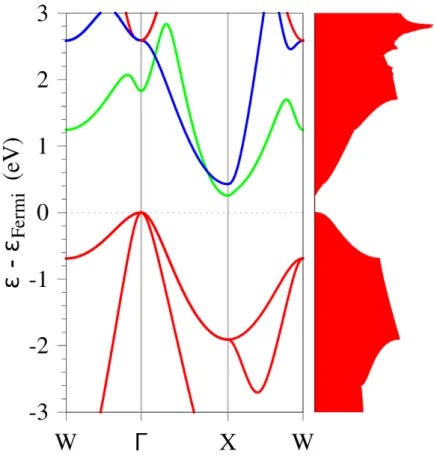
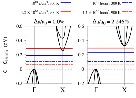
Figure 1 shows the electronic band structures of the bulk Mg2Si. The path is plotted along the high
semiconductor, its electronic band structure presents an indirect band gap, where the valence band maximum (VBM) and the conduction band minimum (CBM) are located at the Γ and X k-points, respectively. The band gap energy along the Γ − X line amounts to about 256 meV, which is underestimated by about 500 meV with respect to experimental data [20] but in agreement with previous theoretical calculations (e.g., [21, 22]). The band structure shows also that the direct band gap is located at Γ with an energy of about 1830 meV. In addi-tion, the two energy-lowest conduction orbitals present a threefold degeneracy and are separated by an energy of 173 meV at the X k-point. These two sets of orbitals tends to converge towards each other, as described in the next paragraph, when the compound undergoes tensile strain.
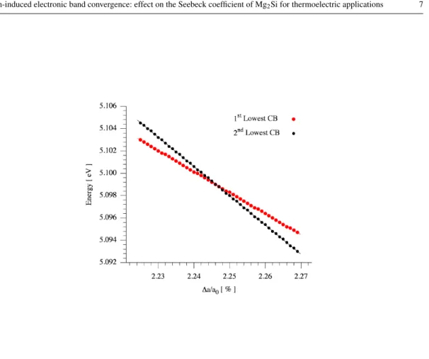
Figure 2 presents the evolution of the energy of the two lowest conduction orbitals at the X k-point with respect to the isotropic tensile strain. It can be seen that the isotropic tensile strain leads to a band crossing resulting in a sixfold degenerated conduction orbital for the ∆ a/a0values of 2.246 %.
In the next sections the calculation of the properties of the constrained material are performed using this value of the isotropic tensile strain.
3.2 Band structure and transport properties under constraint
3.2.1 Band structure
Figure 3 shows the electronic band structure of strained Mg2Si with ∆ a/a0= 2.246 %. Under this constraint
the conduction bands especially at the X k-point are modified compared with those of the strain-free Mg2Si
(Figure 1). The changes in the conduction bands cause an increase of the indirect band gap up to 327 meV and a decrease of the direct band gap down to 1444 meV.
The electronic density of states (DOS) of both the energy-highest valence band (VB) and energy-lowest conduction band (CB) for unstrained and 2.246%-strained Mg2Si is presented in Figure 4(a). The comparison
of the DOS between the strained and the unstrained compound shows that the strain does not noticeably affect the shape of the valence band near the Fermi level Ef as the strained and unstrained Mg2Si VB curves are
superimposed. They depart from each other only at −0.5 eV below Ef. Overall the DOS of the valence band is
slightly shrinked. From the figure 4(b) it can be seen that the convergence of the conduction bands results from both the upshift and downshift of the first lowest CBM (CBM1) and second lowest CBM (CBM2), respectively.
3.2.2 Seebeck Coefficient
This section presents the influence of the convergence of the conduction bands, caused by 2.246 % isotropic tensile strain, on the Seebeck coefficient of the Mg2Si compound. Since the relaxation time (τ) has been
Fig. 2 Calculated energies of the first and the second minimum of conduction bands at X -point as a function of the isotropic tensile strain.
systems. This allows for a reliable comparison between the strained and strain-free Mg2Si bulk property. The
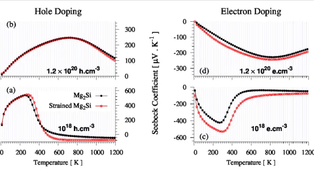
Seebeck coefficient (S) is first given at predefined temperatures and various electron (n-type material) and hole (p-type material) doping levels. As a second step, the evolution of S with respect to temperature and at fixed doping levels (1018and 1.2×1020cm−3) is presented. These concentrations have been chosen from the fact that the Seebeck coefficient of strain-free Mg2Si exhibits its highest values at 300 K for 1018cm−3(electrons
Fig. 3 Electronic band structure (left) and total density of states (right) of the strained bulk Mg2Si under 2.246% tensile strain.
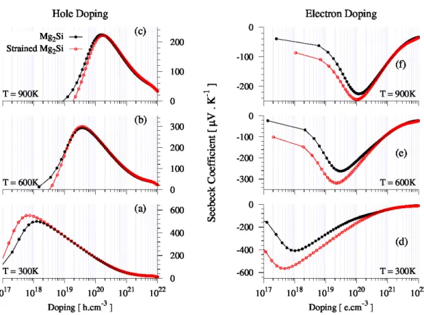
The evolution of S at the three defined temperatures of 300, 600 and 900 K is presented in Figure 5, where the left and right panels refer to the hole and electron dopings, respectively. Irrespective of the type of doping the maximum of S decreases with increasing temperature and shifts toward high doping level. Indeed, at 300 K bulk Mg2Si shows a maximum S value of about 500 and -407 µV.K−1at ∼1018cm−3for hole and electron
doping levels, respectively. As the temperature increases up to 900 K these maxima decrease down to about 224 and -225 µV.K−1at ∼1.2 ×1020cm−3for hole and electron doping levels, respectively.
Due to the marginal deformation on the valence bands, the Seebeck coefficient for hole doping (p) seems to be almost the same for the strained and unstrained Mg2Si, especially for p above 2×10¹⁸, 1019and 1020h.cm−3
(a) DOS of the energy-highest valence band (last VB <HOMO>) and the energy-lowest conduction band (first CB <LUMO>).
(b) DOS of energy-highest valence band (VB), first energy-lowest and second energy-lowest conduction bands (CB)
Fig. 4 Density of states of the strain-free and 2.246%-strained Mg2Si.
for 300, 600 and 900 K, respectively (Figure 5 a − c). We note that, at low temperature (300 K) and hole doping (p < 2 × 10¹⁸h.cm−3) the strained structure shows Seebeck values higher than the bulk Mg
2Si, and
amounts to 552 µV.K−1. This increase could be due to the band gap enlarging. Since the convergence of the bands occurs in the conduction bands, a good enhancement of the Seebeck coefficient of the n-type material is expected. This is indeed what is observed in Figures 5 d − f ; Irrespective of the temperature and for n < 2 × 10²⁰e.cm−3the strained structure shows the highest values of S. In order to highlight further this feature, the improvement percentage of Smaxunder isotropic tensile strain for n− and p−type materials is plotted as a
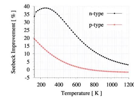
function of temperature in Figure 6. The largest improvement is in favor of the n−type material for which it reaches its maximum of 39% at 300 K.
As the temperature increases the improvement decreases down to below 5 % at high temperature. As can be seen in Figure 7, this feature is ascribed to the position of the chemical potential with respect to the bottom of the conduction band. At 300 K the chemical potential is 50 meV and 80 meV below the bottom of the CB for unstrained and strained Mg2Si, respectively, hence the improvement in S is large. At high temperature,
Fig. 5 Seebeck coefficient of the strain-free and 2.246%-strained Mg2Si as a function of the electron and hole doping level at three
defined temperatures of 300, 600 and 900 K.
explains the low S value. Under isotropic constraint the gap increases, hence the chemical potential is shifted inside the band gap at 30 meV below the bottom of the CB. Therefore, S is improved, though less than at low temperature for which the distance to the bottom of the CB is larger (80 meV).
Figure 8 presents the evolution of the Seebeck coefficient as a function of temperature at constant hole and electron carrier concentrations of 1018cm−3and 1.2 ×1020cm−3, where the left and right panels refer to
the hole and electron doping, respectively. For the strain-free structure, at low temperatures and low doping levels, the Seebeck coefficient reaches values of about 540 µV.K−1for hole doping while for electron doping it reaches about -425 µV.K−1(Figure 8 a, c). However, for temperatures above 400 K, due to the bipolar intrinsic regime, the Seebeck coefficient rapidly drops and levels off to a small negative value (-50 µV.K−1). For the
Fig. 6 Improvement of the Seebeck coefficient with respect to temperature under isotropic tensile strain.
heavy doping level, the maximum of S decreases compared with the low doping case and shifts toward the high temperature domain around 800 K (Figure 8 b, d).
3.2.3 Electrical conductivity
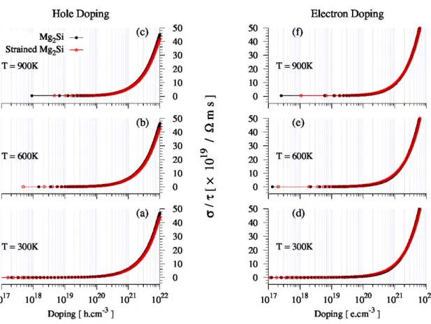
The evolution of the electrical conductivity with the doping level for the unstrained and 2.246%-strained struc-ture is shown in Figure 9. Basically, there seems to be no change in the electrical conductivity whether Mg2Si
undergoes constrains or not. In fact, a slight increase of σ of at most 17% (at 900 K and electron doping of 1.2x1020cm−3) is observed from the calculated data. As to the variation of σ with the doping level, we observe a constant increase, typical for semi-conductors and heavily doped semi-conductors.
3.2.4 Effective masses
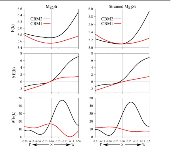
The band effective mass (BEM), which is proportional to the inverse of the second derivative of the band en-ergy (∝ 1/(dE2/d2k)), is known to play a crucial role in the effectiveness of materials for electronic transport
Fig. 7 Energy of the chemical potential in the band structure at various hole and electron concentrations and temperatures.
the thermoelectric efficacy via the quality factor β . By constrast, large BEM contributes to large Seebeck coef-ficient. In Figure 10 is depicted conduction band structure around the X k-point and its successive derivatives for the unstrained and 2.246%-strained structure. It can be first noticed that, for unstrained Mg2Si both the
CBM1 and CBM2 conduction bands have their minimum slightly shifted away from the X k-point by 0.01 Å−1 in the direction of Γ . Second, the mass of CBM1 is larger than that of CBM2 at X k-point (bottom panels in Figure 10). Upon strain, the CBM2 minimum remains slightly shifted from X whereas that of CBM1 is located at the X k-point.
The change in CBM1 and CBM2 mass induced by the strain is opposite for each band: the mass of CBM1 increases by about 65% whereas that of CBM2 decreases by about 20% (Figure 10). Overall, the DOS effective mass, given by m∗= Nv2/3m∗b, where Nvthe pocket degeneracy and m∗bthe average BEM, is increased, which
Fig. 8 Seebeck coefficient of the strain-free and 2.246%-strained Mg2Si as a function of temperature for two electron and hole
doping levels of 1018and 1.2×1020cm−3.
contributes to the improved Seebeck coefficient when Mg2Si is subjected to the isotropic tensile strain (Figure
8 (c) and (d)).
3.2.5 Power factor
The power factor has been calculated from the results presented above for the electrical conductivity and the Seebeck coefficient. The improvement of the Seebeck coefficient is responsible for the increase in the power factor. This is particularly visible at low temperature (300 K) for electron doping for which, a 50% gain is observed (Figure 11(d)). As the temperature increases the gain becomes less (Figure 11(e)-(f)). In addition, under tensile strain the thermoelectric operating temperature of the material is downshifted. This type of behaviour has already been observed for Mg2Si under biaxial strains [23]. For hole doping, since the
effective mass of the valence band is not modified under strain, the Seebeck coefficient remains unmodified, and so is the power factor, irrespective of the temperature (Figure 11(a)-(c)). Hence, we expect an improvement of the thermoelectric response of Mg2Si only in the case of electron doping.
Fig. 9 Electrical conductivity of the strain-free and 2.246%-strained Mg2Si as a function of hole and electron doping levels.
3.2.6 Figure of merit
To estimate the figure of merit zT , the knowledge of the thermal conductivity κ is indispensible. The thermal conductivity is contribute to by a lattice and an electronic parts. In semi-conductors it is generally accepted that the electronic contribution is minor compared to the lattice one, at most one-third of the total κ value at low and intermediate temperature (see e.g. Ref. [24]). The thermal conductivity has not been simulated in this work, hence we rely on experimental data already published (see for instance [24–26]), although these data have been determined for unstrained materials. Roughly, κ varies between 4 and 10 W m−1 K−1[24] depending on the temperature and carrier concentrations.
Fig. 10 Conduction band structure (in eV, top panels), first derivative (in eV Å, middle panels) and second derivative (in eV Å2,
bottom panels) for strain-free and 2.246%-strained Mg2Si. The two, lowest conduction bands (CBM1 and CBM2) are depicted at
the vicinity of the X -point and the band structure is plotted along the Γ (left) and W (right) paths. The units along the abscissa are in Å−1.
Another approximation has to be made in regards to the relaxation time τ of the electrons that intervenes into the calculated electrical conductivity. Recalling that the constant relaxation time approximation of the Boltzmann theory leaves τ undefined, the relaxation time can be determined by comparing the experimental electrical conductivity and the calculated one. According to Akasaka et al. [24] the electrical conductivity amounts to 1.05x10⁵S m−1at 600 K for n=1.38x10²⁰e.cm−3. In the same conditions the calculated σ /τ value is 0.127x10²⁰S m−1s−1for strain-free Mg2Si. Hence τ equals 8.265x10⁻¹⁵s. Assuming an electron-phonon
Fig. 11 Power factor (S2σ ) with respect to electron and hole doping levels for strain-free and 2.246%-strained Mg
2Si at 300 K, 600
K and 900K.
T-dependence of σ and a n-dependence of τ the expression of τ is of the form [27]:
τ = τ0T−1n−1/3 (2)
Using the above conditions for T and n (600 K and 1.38x10²⁰e.cm−3) we obtain τ0= 2.563 10−5 K cm s
by inverting the previous equation. Because we do not know the experimental electrical conductivity for the tensilely strained structure, we cannot calculate τ0for strained Mg2Si. Hence, in the following we use the same
relation to determine τ for the strain-free and strained conditions. It is consequently possible to determine the thermoelectric data σ and zT . Table 1 gathers all the data calculated from the above relations.
Table 1 Transport properties for strain-free and 2.246%-strained Mg2Si. unstrained strained T(K) 300 600 900 300 600 900 κ (W K−1m−1)∗ 9.5 5.7 4 9.5 5.7 4 n(cm−3) 1018 4 × 10¹⁹ 1.2 × 10²⁰ 6 × 10¹⁷ 4 × 10¹⁹ 1.2 × 10²⁰ τ (10−14s−1)∗∗ 8.543 1.249 0.5773 10.128 1.249 0.5773 σ (103S m−1)∗∗ 5.597 44.742 66.579 6.935 54.835 78.102 S(µV K−1)∗∗ -388 -258 -225 -558 -299 -242 zT∗∗ 0.027 0.32 0.76 0.068 0.52 1.03 zT∗ 0.05 0.25 0.7 – – –
∗Experiment from [24].∗∗Calculated, this work.
As expected, the electrical conductivity increases with temperature whereas the Seebeck coefficient de-creases. Overall, the figure of merit increases too, and is larger for strained than for unstrained Mg2Si at a
given temperature. The improvement is particularly noticeable at 900 K where the increase is of about 25 %. This behaviour is mainly caused by both the larger absolute value of S and the larger value of the electrical conductivity for the strained structure.
As compared with the experimental data [24] our calculated values for zT are smaller at 300 K and in good agreement at 600 K and 900 K (Table 1). The higher the temperature the smaller the difference. The deviation is probably caused by the various approximations used in our calculations.
4 Conclusion
The conduction bands overlap at the X k-point of Mg2Si has been achieved through a tensile isotropic strain of
2.246% applied to the structure. Based on DFT and Boltzmann transport theory formalisms a detailed analysis of the electronic properties of the strain-free and strained structure has been done. Under strain an enlargement of about 71 meV of the indirect band gap Γ − X has been observed. The curvature of the valence band is barely modified by the constraint whereas that of the conduction band is notably affected. Upon strain the
effective mass of the electrons is increased by about 80%, which contributes to the improvement of the Seebeck coefficient as compared with the unstrained case. The enhancement of the Seebeck coefficient reaches up to 40 % at low temperature for the n-type material. The figure of merit zT has been calculated with the help of the experimental thermal conductivity and the theoretical electrical conductivity that has been calculated from the relaxation time estimated at various temperatures and electron concentrations. It has been observed that, at a given temperature, upon strain the electrical conductivity increases. Overall, the increase of both σ and S leads to a significant improvement of the figure of merit at all temperatures.
Ackowledgements
This work was granted access to the HPC resources of CINES (Centre Informatique National de l’Enseignement Supérieur, Montpellier, France) under Allocation C2015086881 made by GENCI (Grand Equipment National de Calcul Intensif). This work was also supported by the computing facilities of the CRCMM (Centre Régional de Compétences en Modélisation Moléculaire de Marseille) and by the mésocentre d’Aix-Marseille Université (Project 13b020). The Fondation EADS is acknowledged for financial support of H.B.’s PhD thesis.
References
1. D. Rowe (Ed.), Thermoelectrics Handbook: From Macro to Nano, CRC Taylor & Francis Group, LLC, 2006. 2. I. Ioffe, Semiconductor Thermoelements, and Thermoelectric Cooling, London: Inforsearch, 1957.
3. J. P. Heremans, B. Wiendlocha, A. M. Chamoire, Energy & Environmental Science 5 (2012) 5510–5530.
4. G. Tan, F. Shi, S. Hao, H. Chi, T. P. Bailey, L.-D. Zhao, C. Uher, C. Wolverton, V. P. Dravid, M. G. Kanatzidis, Journal of the American Chemical Society 137 (2015) 11507–11516.
5. Y. Pei, X. Shi, A. LaLonde, H. Wang, L. Chen, G. J. Snyder, Nature 473 (2011) 66–69.
6. Y. Tang, Z. M. Gibbs, L. A. Agapito, G. Li, H.-S. Kim, M. B. Nardelli, S. Curtarolo, G. J. Snyder, Nature Materials 14 (2015) 1223–1228.
7. H.-Z. Li, R.-P. Li, J.-H. Liu, M.-J. Huang, Physica B: Condensed Matter (Amsterdam, Netherlands) 479 (2015) 1–5. 8. G. D. Mahan, J. O. Sofo, Proceedings of the National Academy of Sciences 93 (1996) 7436–7439.
9. T. E. Humphrey, H. Linke, Physical Review Letters 94 (2005) 096601. 10. R. P. Chasmar, R. Stratton, Journal of Electronics and Control 7 (1959) 52–72.
11. H. Balout, P. Boulet, M.-C. Record, Intermetallics 50 (2014) 8 – 13.
12. H. Balout, P. Boulet, M.-C. Record, Journal of Electronic Materials 43 (2014) 3801–3807.
13. P. Villars, K. Cenzual, Pearson’s Crystal Data: Crystal Structure Database for Inorganic Compounds, ASM International Ma-terials Park Ohio USA, 2010-2011.
14. P. Hohenberg, W. Kohn, Physical Review 136 (1964) B864 – B871. 15. W. Kohn, L. J. Sham, Physical Review 140 (1965) A1133–A1138.
16. P. Giannozzi, S. Baroni, N. Bonini, M. Calandra, R. Car, C. Cavazzoni, D. Ceresoli, G. L. Chiarotti, M. Cococcioni, I. Dabo, A. D. Corso, S. d. Gironcoli, S. Fabris, G. Fratesi, R. Gebauer, U. Gerstmann, C. Gougoussis, A. Kokalj, M. Lazzeri, L. Martin-Samos, N. Marzari, F. Mauri, R. Mazzarello, S. Paolini, A. Pasquarello, L. Paulatto, C. Sbraccia, S. Scandolo, G. Sclauzero, A. P. Seitsonen, A. Smogunov, P. Umari, R. M. Wentzcovitch, Journal of Physics: Condensed Matter 21 (2009) 395502. 17. D. Vanderbilt, Physical Review B 41 (1990) 7892—7895.
18. J. P. Perdew, Electronic Structure of Solids ’91, P. Ziesche and H. Eschrig (Akademie Verlag, Berlin,1991), 1994. 19. G. K. Madsen, D. J. Singh, Computer Physics Communications 175 (2006) 67–71.
20. R. G. Morris, R. D. Redin, G. C. Danielson, Physical Review 109 (1958) 1909–1915.
21. A. V. Krivosheeva, A. N. Kholod, V. L. Shaposhnikov, A. E. Krivosheev, V. E. Borisenko, Semiconductors 36 (2002) 496–500. 22. H. Balout, P. Boulet, M.-C. Record, Journal of Electronic Materials 42 (2013) 3458–3466.
23. H. Balout, P. Boulet, M.-C. Record, The European Physical Journal B 88 (2015) 1–9.
24. M. Akasaka, T. Iida, A. Matsumoto, K. Yamanaka, Y. Takanashi, T. Imai, N. Hamada, Journal of Applied Physics 104 (2008) 013703.
25. A. H. Awad, K. S. Dubey, Journal of Thermal Analysis 24 (1982) 233–260. 26. Z. Du, T. Zhu, X. Zhao, Materials Letters 66 (2012) 76–78.


![Deposition Process of Amorphous Boron Carbide from CH[sub 4]∕BCl[sub 3]∕H[sub 2] Precursor](data:image/gif;base64,R0lGODlhAQABAIAAAP///wAAACH5BAEAAAAALAAAAAABAAEAAAICRAEAOw==)