DNA Ruler: Enhancing Nanopore Sizing Resolution by Multiple Measurements on
the Same DNA Molecule
By
Yi-Heng Sen
B.S. Electrical Engineering
National Taiwan University, 2004
M.S. Mechanical Engineering
Massachusetts Institute of Technology, 2008
ACAiUsTT3 INSTITUTE
OCT 2 2
2012
LGRAFIES
Submitted to the Department of Mechanical Engineering
in Partial Fulfillment of the Requirement for the Degree of
Doctor of Science
at the
Massachusetts Institute of Technology
September 2012
C 2012 Massachusetts Institute of Technology, all rights reserved
r,\
Signature of Author:
Certified by:
Accepted by:
Department of Mechanical EngineWing
July 10th, 2012
Rohit N. Karnik
Associate Professor of Mechanical Engineering
is Advisor andom ttee Chair
David E. Hardt
Professor of Mechanical Engineering
Chair, Departmental Committee on Graduate Students
DNA Ruler: Enhancing nanopore sizing resolution by multiple
measurements on the same DNA molecule
By Yi-Heng Sen
Submitted to the Department of Mechanical Engineering
on June 2 9tIh 2012 in partial fulfillment of the
requirement for the Degree of Doctor of Science in Mechanical Engineering
Abstract
Nanopores are versatile sensors for label-free detection of single molecules and particles that have attracted attention for applications such as DNA sequencing and nanoparticle analysis. Detection of single molecules or particles in nanopores is enabled by monitoring the ionic current through the pore: translocation (passage) of a molecule through the pore results in a measurable transient modulation of the ionic current. However, compared to methods such as electrophoresis, nanopores have a limited capacity to discriminate between DNA molecules of different lengths, which have important applications including genornic analysis, DNA sequencing, fingerprinting, and pathogen detection. This thesis focuses on the development of nanofluidic nanopore devices for enhanced discrimination between DNA molecules of different lengths through statistical averaging over multiple detection events on the same molecule.
Microfluidics-integrated devices incorporating nanopores of dimensions 200 nm x 500 nm x 4 gm and 200 nm x 500 nm x 7 gm were fabricated using soft lithography in polydimethylsiloxane (PDMS). When current through the nanopores was monitored using a Axopatch 200B patch-clamp amplifier, translocation events of single molecules
of DNA (48.5 kbp), T7 DNA (39.93 kbp), and a HindIII enzyme digest fragment of
X-DNA (23.13 kbp) were detected as transient increases in the baseline current due to the excess counterions introduced into the nanopore due to the charge on the DNA molecules. To perform multiple measurements on the same DNA molecule, feedback control using LabVIEW was implemented to identify DNA translocation events in real time and reverse the applied voltage bias driving the DNA translocations. DNA molecules were recaptured into the pore with an estimated probability exceeding 99%, enabling the measurement of multiple translocation events on the same molecule. Numerical simulations using a drift-diffusion model were performed to examine the DNA recapture physics and understand the origins of the high recapture rates in the nanopore devices; the measured DNA recapture time distribution was correctly predicted by the numerical simulations. Statistical averaging on multiple measurements resulted in enhancement of the ability of the nanopore to discriminate between DNA molecules of different lengths from a resolution of -8.5 kbp for single measurements to -4.5 kbp for multiple measurements, which enabled length-based discrimination of molecules in a
To isolate the DNA molecule being measured from the DNA sample being analyzed and to improve device stability, next generation nanopore devices were designed with the aims of better device surface control, capability of trapping and detecting DNA molecules, and performing multiple measurements with neither side of the nanopore exposed to the DNA bulk solution. The SU-8 mold for microchannels and trapping chamber was fabricated with UV photolithography, and nanochannels in silica substrate were fabricated with electron-beam lithography, followed by wet etch and reactive-ion-etching (RIE) technique.
Finally, contrary to DNA translocation signals observed in smaller nanopores, a bidirectional modulation of ionic current was observed during the translocation of DNA molecules through the nanopore wherein the ionic current showed a slight decrease followed by a larger increase. Through experiment and simulation, this bidirectional current modulation was shown to be similar in origin to ionic current rectification in a nanofluidic diode, attributed to the spatially asymmetric charge distribution introduced by the DNA molecule as it moves through the nanopore.
This work has shown that multiple measurements on the same molecule in a nanopore device can enhance the ability of the nanopore to discriminate between long DNA molecules of different lengths. Further development of this approach may enable rapid, label-free, high-resolution electrical sizing of DNA molecules by nanofluidic devices, which has hitherto been largely confined to electrophoresis.
Thesis Supervisor and Committee Chair: Rohit N. Karnik, Ph.D. Associate Professor of Mechanical Engineering
Massachusetts Institute of Technology
Committee Member: Alan J. Grodzinsky, Ph.D.
Professor of Biological Engineering, Electrical Engineering and Computer Science, and Mechanical Engineering
Massachusetts Institute of Technology
Committee Member: Jongyoon Han, Ph.D.
Associate Professor of Electrical Engineering and Computer Science and Biological Engineering
Acknowledgements
First of all, I owe numerous thanks to my thesis advisor, Professor Rohit Karnik, for his guidance, encouragement, intellectual wisdom, and professional support. He is one of the nicest people to have as an advisor, and I deeply appreciate his guidance. Without this opportunity, I would not have finished my masters and doctoral degree at MIT.
I would like to thank all of my group members for their help. I am grateful to work together with them. I would like to thank my friends, who have helped me and made my life colorful. I would like to thank Mechanical Engineering department, Microsystems Technology of Laboratories, and Research Laboratories of Electronics.
Finally, I would like to express my deepest appreciation to my family for their support. No words are sufficient to thank them here!
Table of Contents
L ist o f F ig u res ... 9
List of Tables ... 17
Chapter 1 Introduction to nanopore technology ... 19
1.1 Background: nanopore analytics ... 19
1.2 Nanopore sensor devices... 20
1.2.1 Protein nanopores ... 20
1.2.2 Solid-state nanopores... 22
1.2.3 Sensing in sub-micrometer pores ... 24
1.2.4 Current change during DNA translocation ... 25
1.2.5 Steps involved in DNA translocation ... 26
1.3 Thesis background and motivation... 28
1.3.1 DNA sizing Background... 28
1.3.2 DNA sizing with nanochannels and nanopores... 30
1.3.3 Thesis motivation ... 31
1.4 Thesis Overview ... 34
Chapter 2 Design and fabrication of nanopore sensor device ... 37
2.1 Introduction ... 37
2.2 Fabrication of nanopore device ... 37
2.2.1 Design consideration of the device... 37
2.2.2 Nanopore device dimensions ... 39
2.2.3 Overview of the fabrication process ... 40
2.2.4 Equipment used in the fabrication process ... 43
2.2.5 Fabrication of the master mold... 43
2.2.6 Soft-lithography for the PDM S nanopore device... 45
2.3 Discussion ... 46
2.4 Conclusion...48
Chapter 3 Implementation of feedback control for multiple measurements on the same DNA molecule ... 49 3.1 Introduction ... 49 3.2 Experimental setup ... 50 3.2.1 Hardware setup... 50 3.2.2 LabVIEW algorithm ... 52 3.3 Conclusion...61
Chapter 4 DNA sizing by multiple measurements with feedback control...63
4.1 Introduction...63
4.1.1 Past work on multiple measurements ... 63
4.1.2 Structure of Chapter 4... 67
4.2 Theory for current change due to translocation of X-DNA through a nanopore ... 68
4.3 Experiment for DNA detection and translocation in 7 gm nanopore device...70
4.4 M ultiple measurements on single X-DNA molecules... 72
4.4.1 Experimental setup ... 72
4.4.2 Automated data analysis with M ATLAB code ... 74
4.4.3 M ultiple measurements on single X-DNA molecules... 75
4.4.4 Data analysis on multiple measurements on single X-DNA molecules ... 76
4.5.1 Experimental setup and materials...77
4.5.2 Data analysis of multiple measurements on DNA mixture...78
4.5.3 Examination of DNA dynamics with the aid of multiple measurements ... 82
4.5.4 Correlation of the amplitude of current change during translocation with the magnitude and rate of change of the baseline current... 83
4.5.5 Discussion ... 85
4.6 Multiple measurements on DNA mixture: T7 and X-DNA... 88
4.6.1 Experimental setup, nanopore device, and materials... 88
4.6.2 DNA detection and translocation ... 90
4.6.3 Multiple measurements on k-DNA and T7 DNA mixture...92
4.6.4 Data analysis of multiple measurements...94
4.6.5 Comparison between multiple measurements on a mixture of DNA molecules and single-length DNA molecules ... 99
4.7 Recapture time distribution: simulation and experiment ... 101
4 .8 C o nclu sio n ... 10 6 Chapter 5 Fabrication of silica nanopore devices ... 109
5 .1 M otivatio n ... 109
5.2 Design of silica nanopore device... 109
5.3 Fabrication of silica nanopore device ... 112
5.3.1 Overview of the fabrication process ... 112
5.3.2 Equipment used in the fabrication process ... 113
5.3.3 Fabrication of the silica nanopores... 114
5.3.4 Fabrication of the microchannel mold ... 115
5 .3 .5 D iscu ssio n ... 116
5 .4 C o nclu sio n ... 117
Chapter 6 Dynamic bidirectional current modulation during DNA translocation in a n an o p o re ... 1 19 6 .1 Intro duction ... 119
6.1.1 Past work on ionic current rectification in nanochannels and nanopores. 119 6.1.2 Bidirectional current modulation during DNA translocation... 126
6.2 Experiment and results... 127
6.2.1 Experimental setup and PDMS nanopore device ... 127
6.2.2 DNA translocation signal...128
6.2.3 Bidirectional modulation of ionic current during DNA translocation at different buffer strengths...129
6.2.4 Numerical simulation... 133
6.3 Results and discussion ... 137
6 .4 C o nclu sio n ... 139
Chapter 7 Conclusion and outlook... 141
A p p end ix ... 14 3
List of Figures
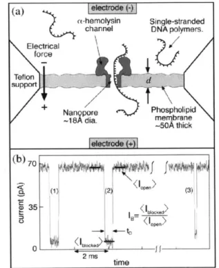
Figure 1.1 Scheme illustrating the principle of nanopore analytics. (a) Single-stranded DNA molecules (negatively charged) and salt ions are electrically driven through a single a-hemolysin protein pore embedded in a phospholipid membrane. Most of the ionic current through the pore is blocked during DNA passage. (b) Three representative translocation current blockades are shown. For each event the translocation time, tD,
and the average event blockade, <IB>, were measured.
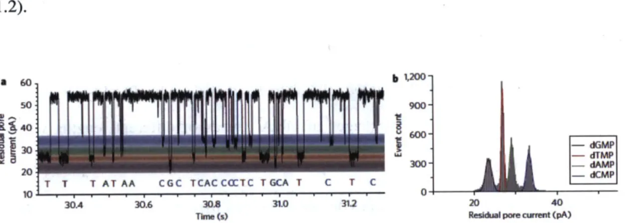
Figure 1.2 Nucleotide event distributions with a permanent cyclodextrin adapter. (a) Single-channel recording from the protein nanopore showing dGMP,
dTMP, dAMP and dCMP discrimination, with colored bands added to
represent the residual current distribution for each nucleotide. (b) Corresponding residual current histogram of nucleotide binding events, including Gaussian fits.
Figure 1.3 DNA transportation and translocation event consist of (X) arrival of DNA molecule from bulk solution, (Y) threading into nanopore, and (Z) passage from entry to end of the pore. Schematic green ball indicates the DNA molecules.
Figure 1.4 (a) Histogram of the ecd observed when the DNA ladder, a mixture of
500, 2027, 2322, 4361, 6557, 9416, and 23 130 bp linear dsDNA was
translocated through a nanopore. The experiment was performed in a 12 nm diameter pore. (b) ecd as a function of DNA length L molecule (kbp). Figure 1.5 Scheme to illustrate the efficacy of multiple measurements. (a) Single
translocation event distributions for two different types of molecules (light and dark lines) may exhibit significant overlap. Observation of a single event is insufficient to distinguish between the two molecules. (b) Distributions of events consisting of multiple translocations will be narrower. Since overlap of translocation event distributions for two different types of molecules significantly decrease, observation of a single event (consisting of multiple translocations of a single molecule) is now sufficient to distinguish between the two molecules.
Figure 1.6 Concept of a device in which multiple translocation events may be recorded for each particle using a nanofluidic system with feedback control, greatly enhancing the resolution of the measurement.
Figure 2.1 Schematic of the process for fabrication of the PDMS nanopore device. Figure 2.2 (a) Overview of PDMS nanopore device. (b) Two microchannels
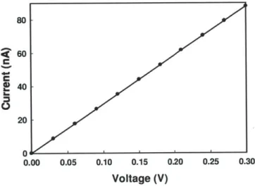
connected by a nanopore of 200 x 500 nm X 4 gm. Figure 2.3 I-V curve of the PDMS nanopore device in IM KCl.
Figure 3.1 Manipulation of DNA molecule in a PDMS microfluidic-nanopore system for multiple measurements with feedback control on a single molecule. (a) DNA in the left reservoir, ionic current value equals to open-pore value. (b) When DNA translocates through the pore, the ionic current increases. (c) DNA in right reservoir, ionic current goes back to open-pore value (d) When DNA traverses through the pore, the ionic current increases. (e)
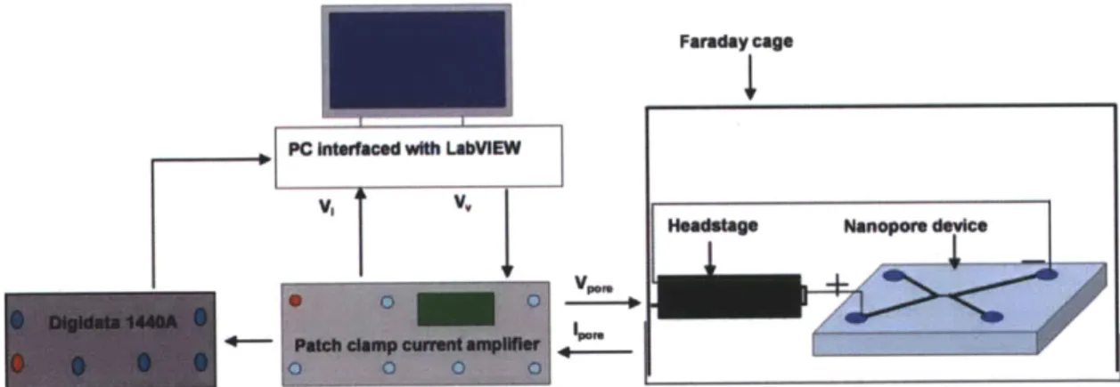
DNA in left reservoir, ionic current goes back to open-pore value. (f) When DNA translocates through the pore, the ionic current increases. Figure 3.2 Experimental setup for measuring the translocation of DNA through a
PDMS nanopore device.
Figure 3.3 Flow chart of feedback control for multiple measurements on the same molecule.
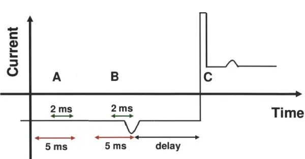
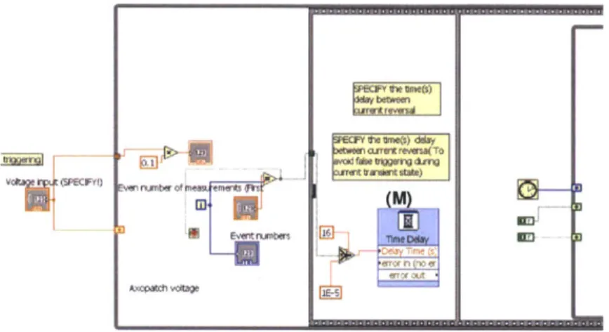
Figure 3.4 Schematic illustration of feedback control. Orange arrow corresponds to open pore nanopore current, black arrow represents real-time ionic current. (A) The algorithm compares real-time ionic current value with open nanopore current to see whether it is larger than open nanopore current. (B) When real time current is larger than baseline current by pre-specified amount, voltage reversal is triggered with a preset delay. (C) After voltage reversal, DNA identification code is paused for a short period of time to avoid transient current region and resultant false trigger. Figure 3.5 Overview of the program consists of (I) Time delay for DNA translocation
identification, (II) DNA translocation identification, and (1II) voltage output and reversal. Red-dashed lines were super-imposed to separate the adjacent blocks.
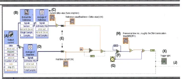
Figure 3.6 Block diagram (II), DNA identification part, of LabVIEW code for
feedback control.
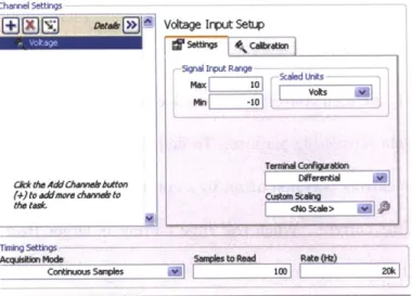
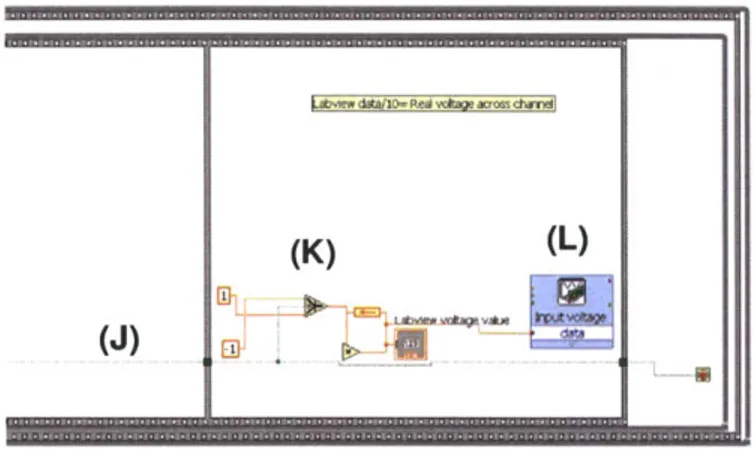
Figure 3.7 Details for "DAQ input" (A) in figure 3.6.
Figure 3.8 Differential terminal configuration rejects common-mode voltage (CMV) noise, thereby increasing measured signal quality.
Figure 3.9 Block diagram (III), voltage output and reversal part, of LabVIEW code for feedback control.
Figure 3.10 Details for "DAQ output" (L) in figure 3.9.
Figure 3.11 Block diagram (I), time delay for ionic current measurement after voltage reversal, of LabVIEW code for feedback control.
Figure 3.12 Interface of the LabVIEW code for feedback control.
Figure 4.1 Experimental configuration DNA multiple translocation by optical tweezer. A tightly focused laser beam is used to trap a DNA-coated bead near a solid-state nanopore immersed in a saline solution (left). Application of a voltage bias drives an ionic current through the nanopore and the negatively charged DNA into the nanopore. When a DNA molecule enters the nanopore (right), an electrical force is exerted on the bead which is displaced to a position where the optical force and the electrical force are balanced.
Figure 4.2 Schematic of the reverse DNA translocation using magnetic tweezers. Two reservoirs, filled with ionic buffer, are separated by a nanopore chip (shown in gray). A voltage bias is applied across the nanopore chip. DNA molecules (shown in red) are attached to the magnetic bead via streptavidin-biotin bonds. Electrical force FE on the DNA and magnetic force Fm on the magnetic bead are depicted in blue.
Figure 4.3 Overview of the recapture experiment. (a) Transmission electron micrograph of the SiNx nanopore used. (b-e) Schematic representation of the experiment. The arrow represents the direction of the electric force on
the DNA molecule. (b) A single DNA molecule passes through the nanopore in the forward direction (c) After passing through the pore, the molecule moves away from the pore under the influence of the electric field for a fixed delay time. (d) The field is reversed, and the molecule moves towards the pore. (e) The molecule passes through the pore in the reverse direction. (f) A representative current trace for an experiment with a 2 ms delay before voltage reversal. A gap of 6.6 nA is omitted from the middle of the trace. The letters mark the correspondence between the current trace and the schematic illustrations of molecular motion (b-e). Figure 4.4 (a) Translocation signal obtained for a 1 pg/mL X-DNA sample with a
voltage bias of -1 V. Current increases by about 15 pA during the translocation due to charge effect. (b) No translocation signals were observed when bias polarity was reversed.
Figure 4.5 (a) PDMS nanopore device consists of two microchannels connected by one nanopore. Negative voltage bias is applied across the nanopore to drive the negatively charged DNA molecule (red) from left to right microchannel through nanopore. (b) After the completion of translocation, voltage bias is reversed to recapture the DNA molecule back to the pore for subsequent translocation. This process continues until the DNA molecule has escaped out of the nanopore, or translocation current signal is not large enough to trigger another voltage reversal. (c) Current trace of multiple measurements on the same DNA molecule of 48.5 kbp X-DNA in 10 mM KCL. For clarity, only 13 out of hundreds of recapture events are shown.
Figure 4.6 Determination of the time DNA enters and exits the nanopore. Black, green, and red dots indicate the time DNA molecule enters, translocates through, and exits the nanopore. Two regression lines were constructed in a time span of 20 ms before and after the translocation event.
Figure 4.7 Scatter plot of translocation time and signal amplitude of multiple measurements (N = 432) on the same DNA molecule. Red dots indicate translocation events, while blue dots indicate the average of 6 consecutive events. The fitted Gaussian curves narrowed down significantly after averaging over multiple measurements, hence increasing the resolution of nanopore system.
Figure 4.8 (a) History of current change of a mixture of DNA (1 gg/mL X-DNA and I gg/mL HindIII digest fragments) Inset: History of current change with only 1 [tg/mL X-DNA in solution does not show abrupt changes in the current. (b) Scrambling the order of the original data followed by
statistical averaging.
Figure 4.9 Comparison between scatter plots and histograms with and without averaging of current change and duration obtained for a solution with only
48.5 kbp X-DNA and a mixture of 48.5 kbp X-DNA and HindIII digest
fragments. (a) Scatter plot of 48.5 kbp X-DNA before statistical averaging. (b) Scatter plot of a mixture of DNA molecules before statistical averaging. (c) Scatter plots converge into one group after statistical averaging for 48.5 kbp X-DNA molecule. (d) Scatter plot converges into
Figure 4.10 Figure 4.11 Figure 4.12 Figure 4.13 Figure 4.14 Figure 4.15
several groups after statistical averaging for a mixture of DNA molecules. (e) and (f) are histograms of current change upon statistical averaging over every 6 consecutive events for only X-DNA and mixture of DNA, respectively. Histogram converges to one Gaussian peak for single DNA, but splits into multiple Gaussian peaks for a mixture of DNA. However, both analytes yield a distribution of one Gaussian peak without averaging (Inset of figure (e) and (f)). The dominance of larger signals is due to sticky ends, and the fact that the algorithm does not enable feedback of fragments smaller than 10 kbp.
Current vs. time traces during feedback control of a mixture of ?-DNA and its fragments. A single large signal (blue arrows) was seen to break up into one small and one larger signal (small and large red arrows) that translocated together for a few cycles. Since feedback was triggered by a single translocation, at a certain point one molecule was left behind (only one red arrow), but reappeared in the following cycle, and again disappeared. Current reversal was not triggered in the final translocation. (a) First order linear regression line showed no significant correlation between open nanopore current and magnitude of current change during DNA translocation. (b) First order linear regression line showed no significant correlation between rate of current change and magnitude of current change during DNA translocation. (a) First order linear regression line showed a negative correlation between open nanopore current and magnitude of current change during DNA translocation. (b) First order linear regression line showed a negative correlation between rate of current change and magnitude of current change during DNA translocation.
48.5 kbp X-DNA molecules conjugated to each other during translocation. Nanofluidic device. (a) Schematic of device showing inlet and outlet reservoirs and microchannels. (b) Micrograph of the device (dotted area in (a)) showing a 200 nm x 500 nm x 4 pm nanopore that connects the two microchannels. (c,d) Application of a voltage bias across the nanopore drives the DNA into the nanopore. (e,f) Upon completion of the translocation, the voltage bias is reversed to translocate the same molecule in the reverse direction. This process is repeated to obtain multiple translocations of the same DNA molecule through the nanopore.
k-DNA translocation signals in 1/15X PBS in 4 pim PDMS nanopore device.
Current traces with feedback control for a mixture of 1 gg/mL X-DNA and 1 tg /mL T7 DNA. (a) Translocation signal of a single DNA molecule (red arrow). Delay time before voltage reversal is also indicated. (b) Current traces showing multiple measurements presumably on the same DNA molecule. When each translocation event (red arrow) is detected, the applied voltage bias is reversed, resulting in successive recapture and translocation of the same molecule. (c) Current traces over a longer period show sets of translocation events separated by pauses that occur whenever the DNA molecule escapes or the translocation is not identified
by the real-time algorithm. Vertical lines in the plot correspond to transient current changes that occur when the applied voltage bias is reversed, with each vertical line indicating a voltage reversal following detection of a translocation event.
Figure 4.16 (a) Chronological sequence of translocation signal amplitudes exhibits distinct shifts in the mean amplitude between series. Horizontal bars denote mean value of the translocation signal for each series. Histogram of the translocation signal amplitude without any averaging (right). (b) Chronological sequence of translocation current amplitudes after averaging over 32 consecutive measurements within each series accentuates the shifts in the mean amplitude between series. The corresponding histogram of translocation signal amplitudes after averaging over 32 consecutive measurements reveals distinct groups of translocation signals (right). Fit to two Gaussian distributions is depicted; the outlying set is excluded from the fit.
Figure 4.17 Causes of series failure. (a) Double translocation: a second molecule translocating within 50 ms of the first translocation. (b) No Trigger: the real-time algorithm fails to detect the translocation event or has detected a pre-set number of translocations in the series. Consequently, there is no voltage reversal soon after the translocation. (c) False Trigger: LabVIEW falsely detects a translocation event, and initiates a voltage reversal prior to the translocation of the molecule. (d) Escape: no translocation is detected within 500 ms after the last translocation in the series. The red line indicates the 500 ms cutoff wait time.
Figure 4.18 (a) Illustration of the translocation signal amplitudes of X-DNA molecules over 2200 translocation events arranged in chronological order, where the mean value remained relatively constant. (b) Averaging over 32 consecutive measurements narrows the translocation signal amplitude distribution while maintaining a single peak, which agrees with multiple measurements taken on a single type of DNA molecule.
Figure 4.19 Environment for DNA transport around nanopore entry is approximated as spherically symmetric.
Figure 4.20 Numerical solution of the drift-diffusion equation showing the DNA probability distribution during the DNA recapture process when the applied voltage bias is reversed at time to (ms) after translocation. (a) to = 5
ms (b) to= 20 ms (c) to= 32.5 ms (d) to= 50 ms (e) to= 65 ms (f) to= 80 Ms.
Figure 4.21 Experimental histogram and simulation for DNA recapture time distribution (The time between voltage reversal and molecule arrival). Figure 5.1 Design of the silica nanopore device for trapping and multiple
measurement purposes.
Figure 5.2 Schematic fabrication process of silica nanopore device.
Figure 5.3 (a) Silica nanopores. Thick stripes correspond to an array of 15 nanopores with 1 gm spacing. (b) SU-8 mold for trapping chamber and microchannels. (c) Zoom in on the 4 gm spacing between trapping
chamber and microchannel shows clean gap without unintended connections.
Figure 6.1 Rectifying properties of a single conical nanopore in a PET membrane with the voltage applied on the base side and the tip side grounded. (A) I-V characteristics obtained under symmetric ion concentration at pH 8 and 3 M KCl (solid circles), 1 M KCl (empty squares) and 0.1 M KCl (empty triangles). (B) I-V curves recorded under symmetric 0.1 M KCl at pH 8 (solid squares) and pH 3 (empty triangles).
Figure 6.2 Rectifying effect due to the disparate ion distribution along the nanochannel having negative surface charge and under different polarities of applied potential. The gray scale plots show the relative ionic concentration in different regions of the channel. (a) High concentration
CH side is positively biased relative to the low concentration side CL. (b) Zero bias. (c) CH is negatively biased. The gray region within the nanochannel that is bound by the dashed lines represents the electric double layers (EDL).
Figure 6.3 (a) Schematic diagram of a nanofluidic diode consisting of a positively charged surface and a neutral surface in different halves of the channel. The positive charge is produced by avidin, while the neutral charge is produced by biotin moieties. (b) Epifluorescence image shows fluorescently labeled avidin in the left half the nanofluidic diode. (c) Theoretical predictions of the ionic concentration and electric potential profiles along nanofluidic diode calculated using the one-dimensional model. The avidin half of the channel has a positive charge of 3 mC/m2, and the biotin half is neutral. (Top) Under forward bias of 5 V, there is concentration enhancement in the channel. (Bottom) Under a reverse bias of -5 V, there is concentration depletion in the channel, and the electric potential drops sharply at the junction of positive and neutral surface charge. Channel height is 30 nm, and KCL concentration is 10 mM. (d) Nanofluidic diode I-V characteristics at different KCl concentrations. Solid circles represent experimental data, while the dashed line has slope equal to the conductance measured using a voltage bias range of -50 to 50 mV. Solid lines are theoretical predictions. Biotin side is at a higher potential under forward bias.
Figure 6.4 (a) Schematic of DNA (in red) with a surrounding EDL (in blue) in a nanochannel, and the location of the CP-induced ion-depletion (between planes 1 and 2) and ion-enrichment (between planes 3 and 4). The arrows (in blue) depicting the cationic current are located inside the nanochannel and are directed from left to right, whereas the arrows (in red) depicting the anionic current are located inside the nanochannel and are directed from right to left. (b) The different dimensions corresponding to the DNA transport in a nanochannel. (c) (left) Schematic of the event of a DNA entering a nanopore (radius R), and the locations of the planes 1 and 2 in between which ion depletion will occur. (c) (right) Schematic of the event of a DNA (shown in red) exiting a nanopore, and the locations of the planes 3 and 4 in between which ion enrichment will occur. (d) The
different dimensions corresponding to the DNA translocation in a nanopore, having radius R.
Figure 6.5 (a) PDMS nanopore device (b) DNA translocation signature indicates both conductance depletion followed by conductance enhancement (c) Current trace showing consistent bidirectional current modulation. Here X-DNA of 1 gg/mL was dissolved in 1/15X PBS, and the voltage bias was 0.7 V. Figure 6.6 (a) In the first half of the DNA translocation, part of the negatively
charged DNA molecule resides in the left half of the nanopore. (b) During the second half of the translocation event before exiting the nanopore, the DNA molecule presents an excess negative charge on the right side of the
nanopore.
Figure 6.7 Histograms for relative current change at (a) 1/15X PBS (b) 1/30X PBS, and (c) 1/60X PBS. Each inset shows a conductance rectification signature (ionic current trace normalized by baseline current) induced by DNA translocation at each buffer concentration.
Figure 6.8 Current increase and decrease v.s. magnitude of voltage bias during single
X-DNA translocation in (a) 1/15X PBS (b) 1/30X PBS, and (c) 1/60X PBS.
The absolute magnitudes of current increase and decrease remained nearly independent of the buffer strength and applied voltage. (d) Baseline current v.s. voltage relationship of PDMS nanopore device at each buffer concentration.
Figure 6.9 The numerical model for ionic transport within nanopore. a-2 denotes the negative surface charge between X, and X2, and its magnitude equals the addition of inherent nanopore surface charge and negative charges from DNA molecule. (3-4 denotes the negative surface charge between X3 and X4, and its magnitude equals the inherent nanopore surface charge.
Figure 6.10 (a) Experimental result for the dependence of conductance enhancement on voltage and buffer concentration (b) Experimental result for the dependence of conductance depletion on voltage and buffer concentration (c) Simulation result for the dependence of conductance enhancement on voltage and buffer concentration (d) Simulation result for the dependence of conductance depletion on voltage and buffer concentration.
List of Tables
Table 2.1 List of MTL and RLE equipment used in the fabrication process for the master mold.
Table 5.1 List of MTL and RLE equipment used in the fabrication process for the silica substrate
Table 5.2 List of MTL and RLE equipment used in the fabrication process for the master mold
Chapter 1 Introduction to nanopore technology
1.1 Background: nanopore analytics
Rapid and accurate sensing of single molecules is an important research topic in many fields such as biology, chemistry, medicine, and forensics'. The capability of detecting and measuring single molecules and other micro/nano scale analytes can lead to the development of rapid diagnostic or analytical/bioanalytical technology. While detection techniques that require labeling analytes with fluorescent molecules are very useful in characterization using microscopy, the requirements of incorporating optics instrumentation and extensive sample preparation steps make it unsuitable for applications that require rapid analysis in a compact system.
Nanopores can detect and characterize analytes by purely electrical signal (Figure 1.1). The working concept of such technology is similar to that of Coulter counter 2; a driving force, either a voltage bias or pressure difference, is applied across the pore while measuring the corresponding ionic current. When analytes pass through the pore, the resulting current change can be used to detect and characterize the analyte.
Research in the nanopore field has been conducted primarily for DNA sequencing application, and several research groups and startups have been developing such technology to achieve rapid and economical DNA sequencing that could meet the $1,000 genome challenge proposed by the National Institutes of Health3. Nanopores for DNA sequencing typically require diameters below 5 nm for molecular-level interactions
4-6
yielding different electrical signals for different nucleotides -6. Devices with larger pore geometry are needed to characterize larger analytes such as viruses, large proteins and protein complexes that fall within the size range of 10-500 nm.
Figure 1.1 Scheme illustrating the principle of nanopore analytics. (a) Single-stranded
DNA molecules (negatively charged) and salt ions are electrically driven through a single
ax-hemolysin protein pore embedded in a phospholipid membrane. Most of the ionic
current through the pore is blocked during DNA passage. (b) Three representative
translocation current blockades are shown. For each event the translocation time,
tD,and
the average event blockade, <IB>, were measured.
1.2 Nanopore sensor devices
1.2.1: Protein nanopores
The field of nanopore research was initiated with the advent of the protein nanopore
formed by a-haemolysin (aHL) from Staphylococcus aureus. In 1996, Kasianowicz et al.
demonstrated that the translocation of single DNA molecules through the naturally
occurring hemolysin pore could be detected by monitoring the ionic current through the
pore8. The protein pore is embedded in a lipid bilayer, and the inner channel diameter of -1.5 nm suggests that only single-stranded DNA is allowed to translocate through a-hemolysin, and only up to a 10 bp fragment can reside in the vestibule at one time. Under electrolyte pH of 7-9, o-hemolysin nanopore forms a stable and reproducible channel with <2% variation in channel dimension?. As the ssDNA molecule passes through the pore, it sterically blocks the pore, resulting in a transient decrease in the ionic current through the pore. With the stability and a size that is just larger than a single stranded DNA molecule, it enables close molecular interactions between the DNA molecule and the nanopore during translocation. Howorka and Bayley 10 engineered this
pore and attached a short DNA strand inside the pore. They were able to infer the electrical potential distribution along the length of the pore by measuring the translocation time and current blockages of DNA strands of different lengths with a sequence complementary to the covalently attached segment. Hemolysin pores could discriminate between current blockages due to purine and pyrimidine segments in a DNA molecule, showing promise for rapid DNA sequencing". Meller et al.5 demonstrated the potential of hemolysin pores to characterize molecules by discriminating between polynucleotide with similar length and composition, but differing only in sequence. Bates et al. studied DNA polymer biophysics by driving DNA molecules into the hemolysin pore and switching off the driving voltage using feedback control and subsequently looking at escape times of DNA molecules from an entropically unfavorable configuration. Wang et al.13 further characterized DNA samples and demonstrated that modifications such as phosphorylation result in different statistical signatures of DNA molecules translocating through hemolysin pores. Clarke et al. used
an exonuclease enzyme to cleave individual nucleotide molecules from the DNA, and
showed that a protein nanopore with a covalently attached adapter molecule can
continuously identify unlabelled nucleoside
5'-monophosphate
molecules with accuracies
averaging 99.8%14. Base selectivity was achieved by modifying the mutant a-hemolysin
pore with a cyclodextrin adapter. Raw bases were read with over 99% confidence under
optimal operating conditions. By integrating this base identification platform with a
highly processive exonuclease, a single molecule sequencing of dGMP, dTMP, dAMP
and dCMP by digestion approach were shown by Oxford nanopore technology (figure
1.2).
60 so T T T AT AA CGC TCACCETC TGCA T C T C b 1,200- 900- 600-300-hIhA
IdAP 30. 30 0. 31.0 3.2 20 40TkM (S) Resi6,a pore curret (pA)
Figure 1.2 Nucleotide event distributions with a permanent cyclodextrin adapter. (a)
Single-channel recording from the protein nanopore showing dGMP, dTMP, dAMP and
dCMP discrimination, with colored bands added to represent the residual current
distribution for each nucleotide. (b) Corresponding residual current histogram of
14
nucleotide binding events, including Gaussian fits'4.
1.2.2 Solid-state nanopores
While protein channels offer a well-defined geometry and are amenable to chemical
modification, they are not amenable to integration with upstream or downstream
processing, and it is difficult to adjust the pore size. These drawbacks resulted in the search for methods to fabricate artificial nanopores that are more robust and give control over nanopore geometry. Li et al.' introduced the method of ion-beam sculpting, in which a 1.8 nm diameter nanopore could be fashioned in a silicon nitride membrane using the bombardment of argon ions to slowly close a larger pore by redistribution of material around the pore. Storm et al.16 demonstrated controlled size reduction of a pore in silicon dioxide using a high energy TEM to fluidize the glass and shrink it due to surface tension. The TEM allowed monitoring of the process and the pore diameter could be controlled down to one nanometer precision. Chang et al.6 fabricated a 50-60 nm
long, 4-5 nm diameter pore using e-beam and standard lithography techniques for 200 bp DNA sensing. Smeets et al.17 studied the dependence of current fluctuations on electrolyte concentration during X-DNA translocation in KCl buffer for 50 mM to 1 M salt concentrations in a solid-state nanopore (length x diameter = 35 nm x 20 nm), which was fabricated with a combination of wet etch, reactive etching, LPCVD, and TEM. Siwy et al.'8 fabricated a conical nanopore using ion track etching technique. This
method entails bombarding a solid material with a collimated beam of high-energy nuclear fission fragments to create parallel damage tracks in the film. The damage tracks are then solution etched into monodisperse cylindrical pores. The diameter of the pores is determined by the etch time, and its density (pores per cm2) is determined by the exposure time to the fission-fragment beam'9. It exhibited a voltage-dependent switching characteristic, similar to biological voltage-gated channels, and was also functionalized with molecular binding agents such as biotin and antibodies and was shown to be capable of highly specific molecule detection. Harrell et al'9 deposited gold in conical nanotubes
embedded inside a polymeric membrane for functionalization with thiolated DNA molecules, and showed that the extent of ionic current rectification could be controlled by either a simple chemical method (varying the DNA chain length) or a simple physical method (varying the nanotube mouth diameter).
1.2.3 Sensing in sub-micrometer pores
Nanopores designed for the sequencing of single DNA molecules need to have small diameters (<5 nm) to detect and linearize DNA molecule conformation during translocation. During single DNA translocation, DNA molecule could exhibit different conformation, and thereby yielding different ionic current behavior for the same type of molecule20. To ensure adequate current signal, the diameter of the pore needs to be made small enough to decrease the transit time of DNA and yield a detectable signal. However, there is a trade-off in terms of fabrication cost, dynamic range, and it is difficult to analyze larger molecules, proteins, or particles of varying sizes using tailor-made nanopores. A few research groups have utilized miniaturized Coulter counter type systems for targeting analysis of particles and colloids in the submicron size range- 2 . In 1977, Deblois et al. demonstrated that viruses above about 60 nm in diameter may be rapidly sized to a few nanometers using 400 nm Coulter counter pore. Saleh et al. used rapid prototyping in PDMS and glass etching to make 200-400 nm nanopores for DNA
26 2
detection and sizing purpose . They demonstrated the detection of A-DNA26, 87 nm
latex colloids23 , and later used this system for detection of protein binding to colloidal nanoparticles for binding assays. The nanopore was used for the detection of human granulocyte colony stimulating factor and granulocyte and macrophage colony stimulating factor27. Other researchers have detected single DNA molecules and
nanoparticles using nanopipettes . Ito et al. used a resistive-pulse Coulter counter based on a membrane containing a single multiwall carbon nanotube channel to simultaneously determine the size and surface charge of 60 nm carboxy-terminated polystyrene nanoparticles, and the resolution was claimed to be comparable to that of transmission electron microscope (TEM)28. Uram et al used 500-600 nm diameter laser machined pores to detect a specific virus or a virus-specific antibody in solution, determine the number of antibodies bound to individual virus particles2 9, and monitor the assembly of
nanoparticles onto templates in situ, all without using fluorescent labeling techniques30 1.2.4 Current change during DNA translocation
Nanopore researchers use conductance modulation during DNA translocation to characterize its chemical or biophysical property. Studies on conductance of nanopore filled with conductive electrolyte have shown its dependence on channel geometry, electrolyte concentration, nanochannel surface charge, and the analyte (DNA molecules, proteins, nanoparticles) that temporarily resides in the nanochannel, 17,2 6. To explain the aforementioned dependence, consider the model where DNA molecule fully stretches inside a nanopore that is filled with KCl electrolyte. The corresponding conductance change A G of such nanopore can be written as 1 7:
AG = (- d DNA PK Cl)nKcle K *,DNA )...1
L Lpore 44
where dDNA (2.2 nm) represents the diameter of the molecule, UK = 7.616 x10⁻⁸ m2/Vs
and p,= 7.9x10 m2/Vs32 are the electrophoretic mobilities of potassium and chloride ions, p*K is the effective electrophoretic mobility of potassium ions moving along the DNA, and q*lDNA is the effective charge on the DNA per unit length, which is assumed to be constant.
Smeet et al. 17 have performed the study of nanopore conductance during DNA
translocation through SiO2 nanochannel at various KCl electrolyte concentrations. They found that depending on KCl concentration, nanochannel conductance could either decrease or increase during DNA translocation. Conductance decrease is attributed to the first term in equation 1.1 due to ion exclusion by the DNA molecule, while conductance increase is attributed to the increase of the concentration of the potassium ions due to the negatively charged DNA molecule. These two effects are competing against each other during DNA translocation. Because the first term, expressing the change in bulk conductance, depends on nKCI, we can expect a linear relationship for delta A G(nKcI) and, hence, a crossover point at which AG = 0. Besides, the crossover was also experimentally verified to occur at KCI = 0.37 M1 7
.
1.2.5 Steps involved in DNA translocation
Figure 1.3 explains the event of DNA molecule transportation to and translocation through nanopore, which consists of three major steps: DNA arrival (X), DNA entrance (Y), and DNA passage (Z). DNA arrival step (X) is the process in which DNA molecule arrives at the entrance of the pore from bulk solution. DNA entrance is the step in which DNA overcomes the entropy barrier, and is about to pass through nanopore. DNA passage step (Z) is the process in which it starts from the completion of DNA capture to the end of DNA passage. Step (X) involves transport via diffusion and electrophoresis from reservoir to the entry of the pore, and the second step (Y) involves DNA molecule threading into the nanopore. When DNA molecule is far away from the pore, the electric field is negligible and the transport of molecule approaching the entrance of the pore is dominated by diffusion3 3
field becomes the dominant factor and attracts DNA molecule further to the entrance of the pore. Subsequently, the DNA molecule overcomes the entropic barrier due to its conformation and threads into the pore. The combination of these two steps determines the rate of DNA capture. Chen et al have shown a linear relationship between magnitude 34 of applied voltage bias and ?-DNA (48.5kbp) capture rate in 15 nm solid-state pore4, while Sen et al. also showed a linear relationship on X-DNA capture rate in 320 nm PDMS pore. Such linear relationship between DNA capture rate and voltage bias
indicates that the DNA arrival step determines the frequency of translocations.
While certain nanopore devices showed the process from reservoir to the pore entrance being the dominant step with linear relationship between voltage and DNA capture rate, other works have shown the exponential relationship between voltage and DNA capture as a result of entropy barrier to DNA entry into the nanopore as being the dominant factor of the entire process. Henrickson et al. have shown the exponential relationship between
36
voltage and capture rate of polyneucleotide in 1.5 nm a-hemolysin pore
The third process (Z) includes the process from the completion of DNA being threaded into the pore to the completion of the entire translocation through the pore. The velocity of the DNA molecule during translocation depends on the size of the pore, the interaction between the nanopore wall and DNA molecule, nanopore surface charge, buffer concentration, and the length of DNA molecule. These three steps comprise the entire process of DNA transportation and translocation event, and the overall analysis throughput of DNA molecule is determined by the slowest of the three.
Figure 1.3 DNA transportation and translocation event consist of (X) arrival of DNA
molecule from bulk solution, (Y) threading into nanopore, and (Z) passage from entry to
end of the pore. Schematic green ball indicates the DNA molecules.
Higher translocation rate implies higher analysis throughput, which is a significant factor
affecting the applicability of nanopore technology. For example, the translocation rate
could be increased by increasing the voltage bias. However, such increase in voltage
magnitude decreases the translocation duration, and therefore decreasing the
characterization resolution.
To circumvent the problem without affecting signal
resolution, Wanunu et al. have found that an ion gradient across the pore can be used to
significantly enhance the magnitude of voltage in the cis chamber, greatly enhancing the
37
DNA capture rate without reducing the translocation times
1.3 Thesis background and motivation
1.3.1
DNA sizing
The ability to accurately measure the nucleic acid length and differentiate nucleic acid
fragments with different lengths has important implications for diverse applications such
as profiling of short tandem repeat (STR) markers38, biomedical diagnostics39, and bio-defense40. Currently the most common approach for DNA sizing is electrophoresis1, which provides high resolution (<lbp) and is the one of the center piece of traditional DNA sequencing technology and other important applications in biochemistry and molecular biology. The electrophoresis method is implemented with a machine that comprises a large matrix or capillary filled with gel material made of agar or polyacrylamide. DNA molecules are injected at one side of the gel, and a voltage bias is applied across the matrix such that these charged DNA molecules will travel through gel medium because of inherent negative charges of DNA molecules as a result of phosphate group (isoelectric point is pH -l). Although DNA molecules of different lengths are known to have uniform electric mobility in free solution, different length of molecules exhibit different mobility inside gel medium due to strong interactions between DNA and the gel network, and shorter DNA molecules with higher electric mobility travel further distance under voltage bias of a set period of time, and molecules of different lengths can be separated and sized with the optical readout for the positions of the fluorescent-tagged
42 DNA molecules
Several disadvantages of this technology have limited its applications; it requires a large matrix for containing gel material, optical instrument experimental steps required for analysis, billions of DNA molecules to have sufficient optical signal from fluorescent-tagged DNA molecules. These disadvantages result in higher cost, longer analysis time, and limit the mobility of the application such as on-site diagnosis.
With the advent of nanopore technology and microfabrication technology 43, researchers have found promising potentials of sizing DNA molecules on a single chip that contains
nanochannels or nanopores. Nanopore technology has nano-meter scale features and requires only electrical signal for yielding molecular-level physical or biochemical information of the analytes. It presents a great alternative to circumvent the disadvantages in electrophoresis method due to its simplicity in analysis and instrumentation, label-free, portability, and the potential of lower cost if devices are being massively produced.
1.3.2 DNA sizing with nanochannels and nanopores
For DNA molecules separation and sizing application, research groups have used either label-free detections or systems that include optics instrument using nanochannel in SiO2 or Si material. Han et al. used UV photolithography and RIE for fabricating silica channels with its height being 75 nm in thin region and 1.5 gm in thick region, and samples of long DNA molecules (5000 to -160,000 base pairs) were efficiently separated into bands in these 15-millimeter-long channels4 4
. Fu et al. fabricated anisotropic nanofilter array of 1 gm x 55 nm using photolithography and reactive ion etching techniques45. Continuous-flow size-based separation of DNA (50-766 bp) and proteins, as well as electrostatic separation of proteins, was achieved, demonstrating the potential use of this device as a generic molecular sieving structure for an integrated biomolecule sample preparation and analysis system. Chan et al. used e-beam lithography and RIE to fabricate fused silica microfluidic chip, and developed a rapid molecular mapping technology-Direct Linear Analysis (DLA)-on the basis of the analysis of individual
46
DNA molecules bound with sequence-specific fluorescent tags . They validated this technology using the 48.5 kbp X phage genome with different 8-base and 7-base sequence motif tags. The distance between the sequence motifs was determined with an accuracy
of ±0.8 kbp, and these tags could be localized on the DNA with an accuracy of ±2 kbp. Foquet et al. manufactured 270 x 1 gm (height x width) silica channel with the fabrication process being derived from the sacrificial layer method47. It allows fabrication of 1 pm micro/nanostructured fluidics systems that are both extremely complex and have tight dimensional tolerance. The device consists of a closed rectangular channel, with several constrictions having submicrometer dimensions, and the behavior of DNA molecules inside these channels under an applied electrical field was first studied by fluorescence correlation spectroscopy using M13 double-stranded DNA. Campbell used focused ion beam to fabricate 150 x 180 nm capillary channels to study the electrophoretic behavior of single, fluorescently-labeled, molecules of DNA as a function of capillary size, and DNA mobility was found to increase with decreasing cross-section".
1.3.3 Thesis motivation
Potentially, nanopores also offer a platform that is easily integrated with microfluidic devices, and capable of performing label-free quick and accurate real-time analysis on analytes such as single DNA without the need for optical interrogation349
-5 1
. However, the resolution of nanopores to size or map DNA molecules is currently limited by variability in DNA translocation time and conformations, as well as the limited signal-to-noise ratio arising from insufficient measurement time during translocation 5 2 5 3. The
52,54
electron-charge-deficit (ecd) molecule4, which is the measured time integral of obstructed ionic current or the integrated event area, has been shown to account for different folded conformations of the translocating DNA molecule, and serves as a powerful measure of the DNA length or molecular weight. With such method, however,
till date it has not been possible for nanopore sensors to differentiate DNA molecules with lengths differing by less than 30%52 , which is calculated by the length difference of DNA molecules that could be distinguished in figure 1.4.
1200
-
2027+2322
a
U.1
F
't 600-
564
6557
4361
E
wN2
OO941623130
E
0 .- .ma--
.il..
..
2 4 6 2 4 6 2 4 6z
10
100
1000
ecd [ke]
1000
-)
100
ecd -
L
'
00b
l
10 4 6 8 2 4 6 8 2 1DNA length [kbp]10
Figure 1.4 (a) Histogram of the ecd observed when the DNA ladder, a mixture of 500, 2027, 2322, 4361, 6557, 9416, and 23 130 bp linear dsDNA was translocated through a
nanopore. The experiment was performed in a 12 nm diameter pore. (b) ecd as a function of DNA length L molecule (kbp)52
.
A promising approach to overcome this issue is to repeatedly measure the transient current signal of the same molecule, which can result in improved resolution through statistical averaging5. Gershow et al.5 5 first showed recapture of 4-10 kbp DNA
a translocation event, but the DNA molecule recapture rate in their nanopore system was
too low to enable statistical averaging and therefore measurement resolution.
In this thesis, the focus is on the improvement in sizing resolution by statistical averaging
over the same DNA molecule, and differentiation of DNA molecules of different length
with such methodology. The typical approach in nanopore measurement system is to let
the analyte escape into reservoir after single measurement. However, if multiple (N)
measurements were implemented on the same analyte for the translocation duration and
its magnitude of current change, the spread in the distributions would decrease as
1/N5,
permitting the use of such nanopores as sensitive probes for label-free analysis of
nanoscale particles and molecules3351, ,55 (Figure 1.5 and 1.6).(a)
(b)
o
0Observation
Duration or
Observation
Duration or
current change
current change
Figure 1.5 Scheme to illustrate the efficacy of multiple measurements. (a) Single
translocation event distributions for two different types of molecules (light and dark
lines) may exhibit significant overlap. Observation of a single event is insufficient to
distinguish between the two molecules. (b) Distributions of events consisting of multiple
translocations will be narrower. Since overlap of translocation event distributions for two
different types of molecules significantly decrease, observation of a single event
(consisting of multiple translocations of a single molecule) is now sufficient to
distinguish between the two molecules.
L-Time
Figure 1.6 Concept of a device in which multiple translocation events may be recorded
for each particle using a nanofluidic system with feedback control, greatly enhancing the
resolution of the measurement.
1.4 Thesis overview
In this thesis, we focus on characterization and controlling the translocation of single
X-DNA molecules through an artificial PDMS nanopore with the objective of enabling
multiple measurements on the same molecule. The rest of the thesis is organized as
follows. Chapter 2 describes the fabrication of the 4 gm long PDMS nanopore devices.
Chapter 3 describes the experimental setup and software algorithm and interface for the
measurement and feedback control implementation.
Chapter 4 demonstrates that
multiple measurements followed by statistical averaging over the same DNA molecule
enables sizing and differentiation in the DNA mixture of DNA and T7 DNA, and
X-DNA and HindIll-digest X-X-DNA.
Chapter
5
describes the fabrication of SiO
2nanochannel array and the mold for PDMS microchannels. Chapter 6 describes the
experimental result of current rectification phenomenon through nanopore device during
DNA translocation, and its analytic model as well as numerical simulation. The final
concluding chapter covers the ongoing work, and suggestions for future directions and work to enhance the performance and capabilities of our DNA ruler system.
Chapter 2 Design and fabrication of nanopore sensor device
2.1 Introduction
Biological nanopores (e.g. a-hemolysin) and artificial solid state nanopores are the two main categories of nanopores . As stated earlier, solid state nanopores have advantages over ca-hemolysin nanopores due to adjustability of the solid state nanopore geometry. Besides, they have the potential to be integrated with different functionalities on the same chip, and can withstand a wider range of environmental and chemical conditions.
Below we will first describe the design considerations for both fabrication process as well as the dimensions of our solid-state nanopore device. Afterwards, we will give an overview of the designed fabrication process, the equipment used for fabrication, and details of the fabrication. Last, we will discuss issues encountered during fabrication.
2.2 Fabrication of nanopore device
2.2.1 Design consideration of the device
We aimed at a nanopore device that serves proof-of-concept demonstration of multiple measurements stated in thesis motivation of in Chapter 1. Specifically, the device should posses capabilities listed below:
1. Ability to detect long (>20 kbp) DNA molecules.
2. Simplicity, reproducibility, and ease of fabrication.
3. Ability to fabricate microfluidic reservoirs of large height (>1 pm) on either side of nanopore.
4. Ability to chemically modify the surface.
5. Ability to accurately control ionic concentration without problems such as evaporation.