HAL Id: hal-00670156
https://hal.archives-ouvertes.fr/hal-00670156
Submitted on 14 Feb 2012
HAL is a multi-disciplinary open access
archive for the deposit and dissemination of sci-entific research documents, whether they are pub-lished or not. The documents may come from teaching and research institutions in France or abroad, or from public or private research centers.
L’archive ouverte pluridisciplinaire HAL, est destinée au dépôt et à la diffusion de documents scientifiques de niveau recherche, publiés ou non, émanant des établissements d’enseignement et de recherche français ou étrangers, des laboratoires publics ou privés.
Dielectric layers with gradual properties
K Makasheva, Bernard Despax, Laurent Boudou, G. Teyssedre, Laurence
Ressier, Patrick Pons
To cite this version:
K Makasheva, Bernard Despax, Laurent Boudou, G. Teyssedre, Laurence Ressier, et al.. Dielectric layers with gradual properties. IEEE International Conference on Solid Dielectrics, Jul 2010, Potsdam, Germany. 4 p. �hal-00670156�
Dielectric layers with gradual properties
Kremena Makasheva1,3,*, Bernard Despax1,2, LaurentBoudou1, Gilbert Teyssedre1,2 1
Université de Toulouse; UPS, INPT; LAPLACE (Laboratoire Plasma et Conversion d’Energie); 118 route de Narbonne, F-31062 Toulouse cedex 9, France.
2
CNRS; LAPLACE; F-31062 Toulouse, France.
3
FCS STAE, F-31432 Toulouse, France.
*
kremena.makasheva@laplace.univ-tlse.fr
Laurence Ressier4 4
Université de Toulouse, INSA, UPS, CNRS, LPCNO, 135 avenue de Rangueil, F-31077 Toulouse cedex 4, France
Patrick Pons5,6 5
LAAS CNRS, 7 avenue du colonel Roche, F-31077 Toulouse, France
6
Université de Toulouse ; UPS, INSA, INP, ISAE; LAAS; F-31077 Toulouse, France
Abstract— This work presents results from a study of thin
dielectric layers organized in a structure that behaves as an unified layer with gradual properties. A better understanding of dielectric charging phenomena is aimed at in order to control the conductive properties of the multi-layer system. We first characterize each mono-layer deposited singly on a substrate before the characterization of our multi-layer system. The presented results are for the material and electrical properties of the layers. They are obtained from different diagnostic methods. It was found that such a concept allows modulation of the conductive properties of dielectric materials.
Keywords- insulating materials, dielectric charging, diagnostics, RF MEMS capacitive switches
I. INTRODUCTION
Dielectric charging phenomenon is a subject of research in many works [1, 2] because of the necessity to control or to avoid it in various system-configurations containing insulators. The questions, still open to revise when dealing with thin dielectric layers, are about the origin of the dielectric charging, the charge retention and charge evacuation in the volume or on the dielectric surface.
Similar questions arise when dealing with microelectromechanical systems (RF MEMS). The dielectric layer seems to be the weakest part of this structure. Dielectric charging is the main mechanism responsible for the failure and the low reliability of capacitive switches with electrostatic actuation [2]. Due to the trapping of electrical charges on the surface or in the volume of the dielectric layer, the values of applied voltage for switch actuation are modified in a way that after a certain number of events the switch is out of control. Different dielectric materials (SiO2, Si3N4, Al2O3) have been
tested in order to improve the performance of RF MEMS capacitive switches.
Nowadays the problem of dielectric charging of RF MEMS capacitive switches still persists and demands more intensive work to be done looking for its solution. Our research effort is directed to the study of dielectric charging phenomenon in general and in the improvement of reliability of technological configurations containing insulator layers in particular. We
believe that a promising solution is to be in command of the conductive properties of the dielectric layer in use. The main purpose of our study is to elaborate and characterize dielectric layers (physico-chemical and dielectric characterization) in order to control their conductive properties when they are organized in multi-layer system.
The dielectric layers are deposited by PPECVD (Pulsed Plasma Enhanced Chemical Vapor Deposition). Details on the deposition technique are described in the next section. Diagnostic methods applied in the characterization of layers, the obtained results and the following discussions are given in Section III.
II. EXPERIMENTAL DETAILS
A. Plasma processing
Thin sub-stoeichiometric silicon nitrite-oxide layers (SiOxNy, x<2, y<1) are deposited on Au/Ti (200nm/50nm)
metallized Si (100) wafers in the plasma sustained by a radiofrequency (f = 13.56 MHz) capacitively coupled discharge with power of 5 W, modulated with square pulses of period T = 400 ms and pulse width of 100 ms. The gas mixture contains SiH4, N2O and He and the ratio =[N2O]/[SiH4]
(partial pressure ratio) allows adjusting the silicon concentration in the film [3]. The total gas flow is around 210 sccm. He-component in the mixtures is fixed to 40%. The gas pressure used for deposition is p = 65 Pa. The substrate temperature is kept to 300°C during the deposition process.
To gradually vary the dielectric-layer properties we deposited a SiOxNy multi-layer structure consisted of 4 layers
with different Si concentration each, when varying the value. Our choice of values for the elaboration of the multi-layer system is as follows: = 100, 25, 10 and = 2. High value ( = 100) means that the dielectric layer has properties close to a SiO2 layer. The lower the value, the richer in Si the
dielectric layer is. This multi-layer structure is deposited on intrinsic Si wafer. The choice of intrinsic Si (100) wafer for the multi-layer structure is based on simplicity of material characterization.
Single layers with the same values as for the multi-layer structure have been deposited separately on Au/Ti metallized Si wafers. The corresponding characterization results are presented in the following section.
III. DIAGNOSTIC METHODS, RESULTS AND DISCUSSIONS We have used several diagnostic methods to investigate the physico-chemical and the dielectric properties of as-deposited multi-layer system and separate layers with the corresponding values.
A. Spectroscopic ellipsometry measurements
The layer thickness and composition of separately deposited layers is determined by spectroscopic ellipsometry measurements. We have used a SOPRA GES-5 spectrometer in the spectral range 250-850 nm. As we deal with metallized wafers, we had first to determine the incidence angle, which is the most appropriate one to perform the measurements. The Brewster’s angle for Au varies strongly as a function of the wavelength and this variation determined the need of such assessment. We have found that for our Au metallized wafers the most sensitive and accurate measurements are to be done in the range 68° – 70° of the incidence angle. Our choice was 69°. The simulation of the registered spectra is performed with Winelli, software provided by SOPRA LAB. For the spectra processing we applied Bruggeman approximation [4, 5]. This model is based on the effective medium theory and provides information on the layer thickness and the concentration of different materials in it. To perform the numerical analyses we used optical data provided by the SOPRA library for amorphous silicon (a-Si) and for SiOxNy layer containing 10%
N in it, instead of pure SiO2 as it does not ignore the small N
concentration in the as-deposited layers.
The obtained results of layer thickness and composition are summarized in Table 1. The layer with = 100 does not contain amorphous silicon in it. When decreasing the ratio, the a-Si concentration increases. For -variation from 100 to 10, the a-Si increases twice. The layer with = 2 is silicon rich layer. It contains 26% of a-Si in the matrix of SiOxNy.
TABLE I. THICKNESS AND COMPOSITION OF THE SINGLY DEPOSITED LAYERS
value Results from spectroscopic ellipsometry
Layer thickness Layer composition
100 116.8 nm ± 0.2 nm SiOxNy
25 193.4 nm ± 0.8 nm SiOxNy + 0.7% a-Si
10 353.9 nm ± 0.8 nm SiOxNy + 1.4% a-Si
2 158.3 nm ± 0.5 nm SiOxNy + 26% a-Si
For the multi-layer structure (deposited on Si substrate), an incidence angle of 75° is used for spectra acquisition in the same spectral range. We have applied the Forouhi-Bloomer approximation for the optical dispersion relation [6] in the modeling as it is the only one that can give us somewhat
correct regression of the parameters. We are aware that the obtained thickness is quite approximate (ML = 67.7 nm ± 2.2 nm) as the media is not homogeneous as required from the applied approximation and this value serves only as an indication of the thickness of the whole structure.
B. Transmission Electron Microscopy
Diagnostic technique that gives us the possibility to observe the as-deposited multi-layer structure is the Transmission Electron Microscopy (TEM) in a cross sectional view. To achieve the observation we have prepared specimens transparent to electrons in accordance with the standard procedure: mechanical polishing and Ar+ ion milling. The observation is performed on a field emission TEM, FEI TecnaiTM F20. This microscope is equipped with a corrector for spherical aberration and the Gatan Imaging Filter (GIF) TRIDIEM. The operation voltage is 200 kV.
To obtain the thickness of the multi-layer structure we have used Defocused Bright Field images as described in [8]. The layer thickness is ML = 52.5 nm ± 2.5 nm, which is much more precise than the value obtained from ellipsometry for the multi-layer structure. Moreover, we have compared the results of the layer thicknesses for the single layers. For a single layer the difference between the values obtained from ellipsometry and from TEM is in the error bar, which confirms the diagnostic procedure that we use in ellipsometry.
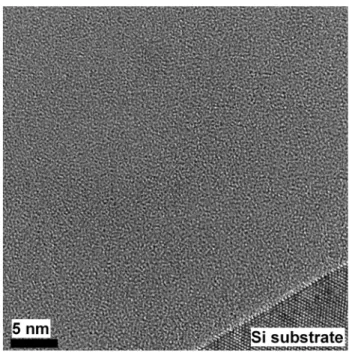
Figure 1. HREM image of the multi-layer structure.
High Resolution Electron Microscopy (HREM) and Energy Filtered TEM (EFTEM) are further performed in our study. Figure 1 presents an HREM image of the multi-layer structure. It clearly shows that the as-deposited multi-layer is in amorphous phase, which certifies the use of optical data for amorphous silicon in the numerical analysis of spectra from ellipsometry and confirms the obtained results.
For EFTEM, we have detected the Plasmon signal (at 17 eV) associated with the Si nanoparticles, as described in [8]. According to the procedure, all the Si nanoparticles with diameter larger than 1 nm, either amorphous or crystalline, are visible and appear as bright in a dark background (the SiOxNy
matrix). EFTEM image of the multi-layer structure is shown in fig. 2. The Si substrate appears in bright. Besides, we can easily distinguish the 4 layers deposited on it, starting with the layer that does not contain a-Si. The thickness of the first three layers ( = 100, 25, 10) is identical. It is d = 13.4 nm for each layer. The thickness of the fourth layer, which is the silicon rich one ( = 2), is d4 = 12.2 nm.
Figure 2. EFTEM image of the multi-layer structure.
C. Fourrier Transform InfraRed Spectroscopy
To complete the structural analysis we have performed Fourrier Transform InfraRed Spectroscopy (FTIR). The infrared spectra were acquired in the 400 – 4000 cm-1 range with BIORAD FTS60A spectrometer. The spectrum of multi-layer system is recorded in transmission mode, as the substrate is intrinsic Si. It is shown in fig. 3.
We can clearly distinguish the Si-O-Si stretching () band at 1023 cm-1 in the spectrum of multi-layer system. In the same range from 400 cm-1 to 1400 cm-1, we can see the Si-N bending () mode in SiN3 configuration at 870 cm-1 [3]. For larger
wavenumbers, an absorption peak at 2253 cm-1 appears. It is associated with the H-SiO3 vibration (). The presence of
Si-H band in the spectrum implies that the film composition can be written as SiOxNyHz. The hydrogen concentration in the film
is difficult to estimate and demands more sophisticated diagnostic methods. Such investigations are of importance since H bonds are involved in the formation of traps for electrical charges.
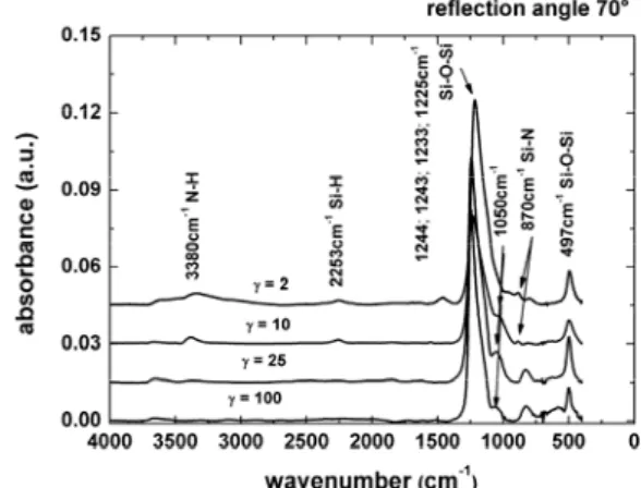
Figure 3. FTIR absorbance spectrum of the multi-layer structure. The infrared spectra of singly deposited layers were recorded in reflection mode at two different angles: 20° and 70° degrees. The necessity of applying the reflection mode comes out from the fact that these layers are deposited on Au/Ti metallized Si substrates. For sake of space saving, only the spectra at 70° are presented (fig. 4).
Figure 4. FTIR absorbance spectrum of the singly deposited layers with different -values ( = 100, 25, 10 and = 2) recorded in reflection mode at
reflection angle of 70°.
When compared to the spectra of singly deposited layers, one can say that the infrared spectrum of the multi-layer system is mainly determined by the last deposited layer ( = 2). For -values larger than = 10, the Si-H and N-H bands disappear. For = 100 the layer is close as composition to SiO2.
D. Electrical charcterization
For electrical characterizations the devices under study were Metal/Insulator/Metal capacitors. A circular golden top electrode of 4 mm in diameter was deposited on the SiOxNy
thin film surface by sputtering, while the ground electrode was the Au/Ti layer, deposited on the Si substrate. The conduction current measurements were carried out under vacuum (10-5-10-6 Pa) at room temperature. Under a step DC voltage application between the top electrode and the Au/Ti layer, the current flowing through the volume was recorded at different electric
fields by a Keithley 617 electrometer. The polarization time was fixed to 1000 seconds and can be considered as leading to a representative conduction current. After each polarization steps the sample was short-circuited for 1000 seconds to recover its initial state.
Figure 5 shows the current vs. field characteristics obtained on the monolayer samples for =2 to 100.
Figure 5. Current density versus Electric Field for different -values. For =2, the measured current density has been divided by 104 for clarity.
The volume resistivity was calculated from current density versus electric field curves (fig. 5) in the ohm's law region, i.e. where the slope of the curve is near unity (dotted lines). The variation of the calculated volume resistivity as a function of is represented in fig. 6 and shows a significant decrease of resistivity when is decreased. Furthermore for values under 10, the decrease of volume resistivity is sharp, and the value for = 2 is much than 6 orders of magnitude lower compared to that for = 100.
Figure 6. Variation of the volume resistivity as a funtion of ratio. The results obtained from electrical characterization are consistent with the results from spectroscopic ellipsometry
where a significant increase of the a-Si concentration in the SiOxNy layers is observed when decreases from 10 to 2.
Moreover they are in-line with the results for the optical gap presented in [3], which refer to silicon nitrite-oxide layers deposited in similar conditions using PPECVD: the optical gap decreases from Eg = 4.0 eV for = 8 to Eg = 2.0 eV for = 2.
IV. CONCLUSION
The structural, physico-chemical and electrical characterizations of silicon nitrite-oxide layers deposited singly or in a multi-layer structure show the possibility to deposit a structure with gradual properties and to modulate the conductive properties of as-deposited multi-layer system. Results from different diagnostic techniques are consistent with each other. The abrupt decrease of the layer resistivity is in accordance with the strong increase of a-Si concentration in the Si-rich silicon nitrite-oxide layer. Experiments are on the way for characterizing multi-layer samples by conductivity measurements along with charge decay in these samples.
ACKNOWLEDGMENT
The authors would like to acknowledge the invaluable help of Dr. Caroline Bonafos (CEMES, Toulouse, France) for the observations and interpretation of the results obtained by TEM.
REFERENCES
[1] C. A. Rezende, R. F. Gouveia, M. A. da Silva, and F. Galembeck, “Detection of charge distribution in insulator surfaces” in J. Phys.: Condens. Matter., vol. 21, 263002, 2009.
[2] M. Lamhamdi, P. Pons, U. Zaghloul, L. Boudou, F. Coccetti, J. Guastavino, Y. Segui, G. Papaioannou and R. Plana, “Voltage and temperature effect on dielectric charging for RF-MEMS capacitive switches reliability investigation” in Microelectronic reliability, vol. 48, 1248, 2008.
[3] M. Bedjaoui and B. Despax “Physico-chemical, Structural and Physical Properties of Hydrogenated Silicon Oxinitride Films Elaborated by Pulsed Radiofrequence Discharge” in Thin Solid Films, in press, Accepted Manuscript. doi :10.1016/j.tsf.2009.11.068, 2010.
[4] D.A.G. Bruggeman “Berechnung verschiedener physikalischer Konstanten von heterogenen Substanzen. I. Dielektrizitätskonstanten und Leitfähigkeiten der Mischkörper aus isotropen Substanzen” in Annalen der Physik, vol. 416, 636-664, 1935.
[5] M. Wakagi, H. Fujiwara, and R.W. Collins “Real time spectroscopic ellipsometry for characterization of the crystallization of amorphous silicon by thermal annealing” in Thin Solid Films, vol. 1, 313-314:464-468, 1998.
[6] A. R. Forouhi and I. Bloomer “Optical dispersion relation for amorphous semiconductors and amorphous dielectrics” in Phys. Rev. B, vol. 34, 7018-7026, 1986.
[7] G.B. Assayag, C. Bonafos, M. Carrada, A. Claverie, P. Normand, and D. Tsoukalas “Transmission electron microscopy measurements of the injection distances in nanocrystal-based memories” in Appl. Phys. Lett., vol.82, 200-202, 2003.
[8] S. Schamm, C. Bonafos, H. Coffin, N. Cherkashin, M. Carrada and G. Ben Assayag “Imaging Si nanoparticles embedded in SiO2 layers by (S)TEM-EELS” in Ultramicroscopy, vol.108, 346-357, 2008.