On the Mutual Effect of Viscoplasticity and Interfacial Damage Progression in Interfacial Fracture of Lead-Free Solder Joints
12
0
0
Texte intégral
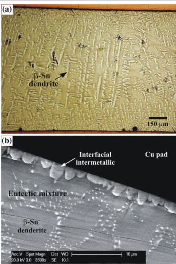
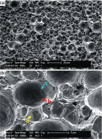
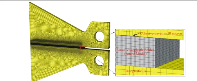
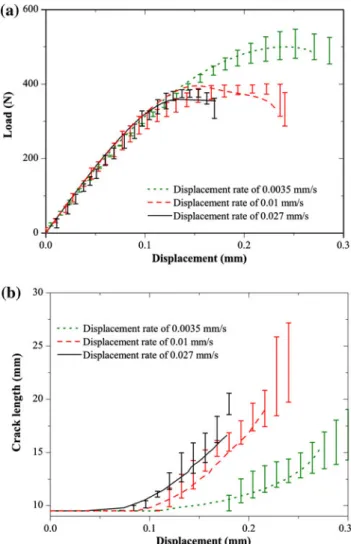
Figure


+5


Documents relatifs
