HAL Id: hal-02883866
https://hal.archives-ouvertes.fr/hal-02883866
Submitted on 29 Jun 2020
HAL is a multi-disciplinary open access
archive for the deposit and dissemination of
sci-entific research documents, whether they are
pub-lished or not. The documents may come from
teaching and research institutions in France or
abroad, or from public or private research centers.
L’archive ouverte pluridisciplinaire HAL, est
destinée au dépôt et à la diffusion de documents
scientifiques de niveau recherche, publiés ou non,
émanant des établissements d’enseignement et de
recherche français ou étrangers, des laboratoires
publics ou privés.
Ultra-low-threshold continuous-wave and pulsed lasing
in tensile-strained GeSn alloys
Anas Elbaz, Dan Buca, Nils von den Driesch, Konstantinos Pantzas, Gilles
Patriarche, Nicolas Zerounian, Etienne Herth, Xavier Checoury, Sébastien
Sauvage, Isabelle Sagnes, et al.
To cite this version:
Anas Elbaz, Dan Buca, Nils von den Driesch, Konstantinos Pantzas, Gilles Patriarche, et al..
Ultra-low-threshold continuous-wave and pulsed lasing in tensile-strained GeSn alloys. Nature Photonics,
Nature Publishing Group, 2020, 14 (6), pp.375-382. �10.1038/s41566-020-0601-5�. �hal-02883866�
Ultra-low threshold continuous-wave and pulsed
lasing in tensile strained GeSn alloys
Anas Elbaz
1,2, Dan Buca
3,*, Nils von den Driesch
3,4, Konstantinos Pantzas
1, Gilles
Patriarche
1, Nicolas Zerounian
1, Etienne Herth
1, Xavier Checoury
1, S ´ebastien Sauvage
1,
Isabelle Sagnes
1, Antonino Foti
5, Razvigor Ossikovski
5, Jean-Michel Hartmann
6,
Fr ´ed ´eric Boeuf
2, Zoran Ikonic
7, Philippe Boucaud
8, Detlev Gr ¨
utzmacher
3,4, and Moustafa
El Kurdi
1,*1Center for Nanoscience and Nanotechnology, C2N UMR 9001, CNRS, Universit ´e Paris Sud, Universit ´e Paris Saclay, 91120 Palaiseau, France
2STMicroelectronics, Rue Jean Monnet 38054 Crolles, France
3Peter Gr ¨unberg Institute (PGI 9) and JARA-Fundamentals of Future Information Technologies, Forschungszentrum Juelich, 52428 Juelich, Germany
4JARA-Institute Green IT, RWTH Aachen, 52062 Aachen, Germany
5LPICM, CNRS, Ecole Polytechnique, Universit ´e Paris-Saclay, 91128 Palaiseau, France 6CEA, LETI and Univ. Grenoble Alpes, 38054 Grenoble, France
7Pollard Institute, School of Electronic and Electrical Engineering, University of Leeds, Leeds LS2 9JT, UK 8Universit ´e C ˆote d’Azur, CNRS, CRHEA, 06560 Valbonne, France
*corresponding authors: moustafa.el-kurdi@u-psud.fr, d.m.buca@fz-juelich.de
ABSTRACT
Strained GeSn alloys are promising for realizing light emitters based entirely on group IV elements. Here, we report GeSn microdisk lasers encapsulated with a SiNx stressor layer to produce tensile strain. A 300nm GeSn layer with 5.4 at. % Sn, which is an indirect band-gap semiconductor as-grown, is transformed via tensile strain engineering into a direct band-gap semiconductor that supports lasing. In this approach the low Sn concentration enables improved defect engineering and the tensile strain delivers a low density of states at the valence band edge, which is the light hole band. We observe ultralow-threshold continuous wave (cw) and pulsed lasing at temperatures of up to 70K and 100K respectively. Lasers operating at a wavelength of 2.5 µm have thresholds of 0.8 kW cm−2for ns-pulsed optical excitation, and 1.1 kW cm−2under cw optical excitation. The results offer a path towards monolithically integrated group IV laser sources on a Si photonics platform.
Introduction
Si-Ge-Sn alloys are a promising, enabling material system for the monolithic integration of both passive and active optoelectronic devices and circuits on Silicon1. Silicon (Si) photonics presently relies on integration of III-V materials for emitters2. Although such an approach has recently demonstrated some impressive progress, it still faces challenges like the wafer throughput, scalability and compatibility with the current Si complementary metal oxide semiconductor (CMOS) technology. The most successful route for laser action within group IV materials nowadays is based on germanium-tin (GeSn) semiconductors. The first demonstration of an optically pumped laser3and subsequent developments to improve the performance in respect to threshold and operation temperature4–7, have shown the potential of these group IV materials for achieving Si-based light sources, the final ingredient for completing an all-inclusive nano-photonic CMOS platform. Furthermore, (Si)GeSn materials can help to extend the present Si photonics platform with a much broader application area than only near infrared data communication. In the short-wave to mid infrared region of 2–4 µm, in which GeSn laser emission has been obtained, potential applications including gas sensing for environmental monitoring and industrial process control8, lab-on-a-chip applications9,10 or infrared imaging for night vision and hyperspectral imaging11can be envisaged.
A Sn content increase in GeSn alloys modifies the energy of the electronic bands. The band-gap at Γ-point (EΓ) reduces faster than the band-gap towards the L-valley (EL), leading to a crossover from an indirect to a direct band-gap semiconductor at an Sn concentration of 8 at. %3. The lattice mismatch between Sn-containing alloys and the Ge buffer layer, the typical virtual substrate for their epitaxial growth, generates compressive strain in the grown layer, which counteracts the effect of Sn incorporation, decreasing the directness ∆EL−Γ= EL− EΓ. On the contrary, applying tensile strain will increase the directness.
Finding a proper balance between a moderate Sn content to minimize crystal defects and to maintain thermal stability of the GeSn alloy on one hand and making use of tensile strain on the other hand are the keys to bring lasing threshold and operation temperature close to application’s requirements. The mainstream research to increase ∆EL−Γfocuses on high Sn content alloys5,12, obtained by epitaxy of thick strain-relaxed GeSn layers. A large directnesss is obtained, leading to higher temperature operation, although at the expense of steadily increasing laser threshold13. We have recently theoretically proposed an alternative approach, which is based on two key ingredients: employing moderate Sn content GeSn alloys, and inducing tensile strain in them14. This study indicated that, if a given directness is reached via tensile strain rather than by increasing Sn content, the material can provide a higher net gain. The underlying physics originates in the valence band splitting and lifting up of the light hole, LH, band above the heavy hole, HH, band. Its lower density of states (DOS) reduces the carrier density required for transparency, hence reduces the lasing threshold, as will be shown below.
GeSn alloys with a moderate Sn content offer a couple of advantages from the materials perspective. The epitaxial growth temperature, 375◦C compared to below 300◦C for high Sn content alloys, yields a better crystalline quality and lower defect density. Lattice mismatch, and therefore, the density of misfit dislocations at the GeSn/Ge interface scales with the Sn content15. Both types of defects strongly influence the carrier recombination dynamics16,17and contribute to the high pumping levels necessary to reach lasing. Accordingly, laser thresholds of 100–300 kW cm−2were reported at 20 K for GeSn lasers with 12–14 at. % Sn4,18, while ∼MW cm−2values are required for very high Sn content alloys (>20 at. %) above 230 K7,12. The described material advantages and the underlying physics should then be combined with the technology able to induce tensile strain in GeSn alloys. Strain engineering is a mature Si technology employed to modify the electronic band structure of semiconductors19. In pure Ge, 1.7 % biaxial20,21or 4.5 % uniaxial22–24strain is required to energetically align the L- and Γ-valleys (∆EL−Γ= 0), i.e. to reach crossover from an indirect to a direct semiconductor. Even higher strain is required to achieve the mandatory directness, ∆EL−Γ>150 meV, for room temperature operation of a strained Ge laser. Although such high levels of tensile strain are technologically possible25,26, they are challenging in a laser device geometry. Depending on Sn content, which can be chosen in the range of 5–8 at. %, significantly lower values of tensile strain are needed in GeSn alloys to achieve a sufficient directness14. However, in order to obtain laser with low pumping threshold, the impact of the defective GeSn/Ge interface region has to be removed. It is responsible for a considerable part of non-radiative recombination. The growth of hetero- and quantum well structures appears to be a suitable technology to separate the gain material from the defective interface17. Here, we focus on the impact of tensile strain and, for simplicity, we are using bulk GeSn layers. To remove the defective interface, the layer transfer method is applied, as used to fabricate GeSn on insulator (GeSnOI) structures. Due to the transfer, the defective part is at the top surface of the GeSn layer and can be easily removed by etching.
All GeSn lasers reported in the literature so far operate only under pulsed excitation, although continuous wave (cw) lasing is the key milestone required for accessing the full potential of GeSn for technologically useful optical devices.
In this work, we demonstrate both cw and pulsed lasing using microdisk cavities fabricated from initially indirect band-gap Ge0.946Sn0.054alloys. Tensile strain of 1.4 % is applied ex-situ to the GeSn layer, using all-around SiNxstressors. The method relies on the formation of GeSnOI by wafer bonding and layer transfer, followed by under-etching so that the final cavity is supported by a metallic post, here Al, that acts as a heat sink. The combination of these factors, i.e. strain engineering, bulk defect density reduction, and improved heat removal, allows the demonstration of lasing in tensile strained GeSn with record low thresholds of 0.8 kW cm−2and 1.1 kW cm−2at 25 K in pulsed and cw operation regimes, respectively. The threshold is two orders of magnitude lower than previously reported for GeSn pulsed lasers, while no reports of cw lasing in GeSn are available.
Results
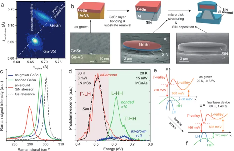
Material growth, characterization and cavity patterning. The GeSn layers were grown on Ge virtual substrates (Ge-VS) on 200 mm Si(100) wafers4,18TRON TRICENT® reactor27. Digermane (Ge2H6) and tin tetrachloride (SnCl4) were used as precursors for elementary Ge and Sn, respectively. GeSn layers with thicknesses of 300 nm and Sn content of 5.4 at. % were grown at 375◦C. The layers were partially strain relaxed, with a residual compressive strain of −0.32 % as measured by X-Ray diffraction (Figure1a). Details on material characterization can be found in the supplementary information (SI).
The GeSn layers were processed into microdisk cavities with all-around SiNxstressors. The technology flow, developed for pure Ge28and adapted for GeSn thermal budget limitations29, is presented in the SI. Yet, some key aspects are shown in Figure1b. The stressor layer is a 350 nm thick SiNxlayer with an intrinsic stress of −1.9 GPa. An additional Al metal layer was added to the layer stack, in order to reduce heating during optical pumping30,31. This is particularly important, since alloying of Ge with Sn strongly decreases the thermal conductivity of the alloy32. After GeSn bonding and removal of the donor wafer, the top 40 nm of the GeSn layer, containing the defective GeSn/Ge interface, was also removed. It was shown that this dense misfit network strongly reduces the photoluminescence of the layers at the onset of strain relaxation33. Up to this step the compressive strain in the GeSn layer is preserved (Figure1c,d). Tensile strain, coming from the SiNxstressor underneath, is induced only by structuring the GeSn/ SiNxlayer stack (Figure1b). The under-etching process, i.e. selective and local removal of Al, was optimized to maximize the tensile strain in the GeSn layer and have a wide Al post for heat sinking. Subsequently,
the suspended disks were conformally covered by a second 400 nm thick SiNxstressor layer, leading to fully encapsulated GeSn disks, standing on Al posts (Figure1b).This layer transfer technology and processing transforms the initial Ge0.946Sn0.054 layer with residual compressive strain having an indirect band-gap into a microdisk exhibiting pronounced biaxial tensile strain and consequently a direct band-gap.
a
280 290 300 Ge reference as-grown GeSn bonded GeSn all-around SiN stressorRaman signal intensity (a.u.)
Raman signal (cm-1) 310 k E HH LH L-valley Γ-valley 720 meV 660 meV as-grown 20 K, -0.32% -30 meV k E HH LH L-valley Γ-valley 466 meV 535 meV
final laser device 80 K, 1.40 % 170 meV
e
f
tensile strain GeSn layer bonding & substrate removalc
b
micro disk structuring & SiN deposition GeSn Ge-VS as-grown aout-of-plane (Å) Ge-VS GeSn 5.60 5.65 5.70 5.75 5.60 5.65 5.70 5.75 ain-plane (Å) pseudomorphic line strain-relaxed line Photoluminescence (a.u.) 0.4 0.5 0.6 0.7 0.8 Energy (eV) bonded x10d
Γ
-HH Sim 80 K 8 mW LN InSbΓ
-LH as-grown x10 20 K 15 mW InGaAs L-HH all-around SiN 2 µm Al SiN GeSn 2 µm 10 nmFigure 1. Structural and optical characterization.(a) X-Ray diffraction reciprocal space map for quantitative assessment
of the layer strain (−0.32 %). (b) Sketch of the processing steps. TEM image of the as-grown layer with strain releasing dislocations at the GeSn/Ge-VS interface. SEM images of the under-etched GeSn/SiNxstack and the final laser structure with SiNxall-around. (c) Raman spectra for three cases: as-grown layer, bonded (i.e. transferred) layer and all-around disk of 9 µm diameter. Bulk Ge is used as reference. (d) PL spectra taken at 20 K for the as-grown and bonded GeSn layers (the bonded layer has the misfit dislocation network removed), and PL of patterned disk with all-around stressor at 80 K. The dotted line shows the simulated PL spectra of the final structure. The calculated band structure for the (e) indirect band-gap as-grown layer and (f) direct band-gap tensile strained GeSn layer.
Sample analysis
Raman spectroscopy was performed to follow the strain evolution during fabrication of GeSn microdisks. The positions of the Ge-Ge vibration modes in GeSn alloys in the as-grown sample (blue line), after bonding onto the host Si substrate (green line), and the final processed microdisk structure are shown in Figure1c. The Raman modes of the unpatterned transferred layer and the as-grown layer, at 297.3 cm−1and 296.8 cm−1, respectively, are very similar, within the experimental resolution of 0.5 cm−1. Therefore, it can reasonably be assumed that the layer transfer process itself does not change the strain in the GeSn layer. However, after the processing of the final microdisk, a Raman shift of −10.5 cm−1is detected. Using the equations from Ref.34, including alloy disorder and strain effects, this Raman shift corresponds to a built-in biaxial tensile strain of 1.5 % for the all-around embedded GeSn disk. Note that Raman spectroscopy probes only the in-plane strain within a small depth below the disk surface, while photoluminescence probes the whole disk volume, giving an average value of the strain, and is directly related to the band structure.28.
Photoluminescence (PL) experiments were conducted to assess the strain-induced band structure changes, as well as the quality improvement of the transferred layer. The PL signal from the as-grown GeSn layer is very weak, due to (i) the
indirect band-gap, with the conduction band energy splitting ∆EL−Γ=−60 meV, and (ii) the presence of defects at the GeSn/Ge interface. After the layer is transferred, these defects are removed and an increase in PL intensity is observed (Figure1d). The PL signal is found in the same energy range, indicating again that the transferred layer maintains its compressive strain and, therefore, its indirect band-gap character with L and HH as conduction and valence band extrema, respectively. The optical transition at 0.61 eV is attributed to the recombination of electrons in the L-valley of the conduction band and holes near the Γ point of the HH valence band, thus across the fundamental indirect band-gap. Indirect carrier recombination dominates over the direct transitions, because almost 100 % of electrons at 20 K are in the L-valley. The shoulder of the PL signal around 0.66 eV is assigned to the direct transition, i.e. electrons and heavy holes around the Γ-point in k-space. Details on optical transition identification can be found in SI. PL spectra in Figure1d for the as-grown and the transferred GeSn layers are taken under identical conditions with a sensitive InGaAs detector. This is emphasized because this, initially weakly-emitting, layer will become the active laser medium after inducing the tensile strain.
The major limitation for the GeSn emission efficiency, the indirect band-gap, is overcome by tensile strain turning it into a direct-gap semiconductor. Since the extended InGaAs detector has a cut-off wavelength of 2.4 µm, another set-up with a nitrogen cooled InSb detector, with a cut-off of 4.8 µm, is used for the fully processed microdisk device. Even though the InSb detector has a lower sensitivity, a strong increase of the integrated PL emission by 2 orders of magnitude compared to the as-grown layer is measured. The PL signal is strongly red-shifted, showing the peak emission around 0.50 eV which is attributed to the tensile strain of the final structure with the all-around SiNxstressor. The band structure was modeled using k·p method, taking 5.4 at. % Sn and a band-gap of 465 meV of the strained film. The best fit to the experimental data in Fig.1d is obtained for biaxial tensile strain of 1.4 %. This value is slightly smaller than the 1.5 % obtained from Raman spectroscopy. The discrepancy is attributed to the uncertainty of the parameters used in the two methods. The band structures of the as-grown and tensile strained GeSn are shown in Figure1e and -f, respectively. In the final device, the tensile strain lifts the degeneracy of the LH and HH band, with LH becoming the fundamental valence band. The valence band splitting is ELH− EHH=170 meV. More importantly, in the conduction band the tensile strain shifts the Γ-valley below the L-valley. The tensile strained GeSn thus becomes a direct band-gap material with a directness of ∆EL−Γ= 70 meV. Consequently, the pronounced enhancement of the PL intensity emission is due to the fundamental direct optical transition. The electrons recombine with LH at the Γ point in the center of the Brillouin zone. This transition is labelled as Γ-LH optical transition.
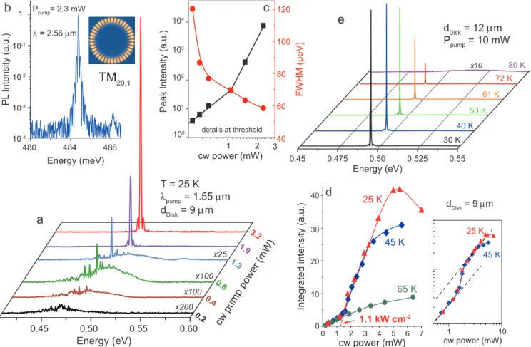
CW device results
In order to obtain stimulated emission, microdisk devices with a diameter of 9 µm were optically pumped using a µ-PL setup with 1550 nm wavelength cw pump laser focused on the sample surface into a 12 µm diameter spot (see Methods). PL emission spectra collected at various incident pump powers at 25 K are shown in Figure2a. At low excitation levels, the microdisks produce a broad spontaneous emission background, attributed to Γ → LH direct transitions. By increasing the cw pump power from 0.2 mW to 0.8 mW, whispering gallery modes (WGM) develop and grow in intensity on top of the spontaneous emission. Higher excitation induces an exponential intensity increase of the main optical mode at 485 meV. At 2.3 mW pump power, the lasing emission is four orders of magnitude stronger than the background, as shown in the high resolution spectrum in Figure2b. The two symmetric side lobes of the modes are only a measurement artifact, which stems from a finite range of sampling points due to the apodization of the interferogram.35
The observation of a clear threshold in the light-in light-out (L-L) characteristic visible in Figure2c,d, the S-shape L-L characteristic (inset Figure2d) and the collapse of the linewidth (Figure2c) unambiguously prove the onset of lasing. The emission energy at 25 K of the lasing mode at 485 meV corresponds to 2.55 µm wavelength. WGM simulations (see Methods) indicate that this mode is the transverse magnetic TM20,1mode. The intensity of this mode in the threshold region is displayed in Figure2c as a function of incident pump power by the linear L-L characteristics. The observed narrowing is consistent with the Schawlow-Townes equations, which predict a decrease by a factor of two at the transition from incoherent to coherent emission. Note that the measured linewidth of 58 µeV is the smallest reported to date for any group-IV semiconductor lasers. The laser threshold, clearly separating the spontaneous and the amplified emission regimes, is extracted as 1.3 mW (Figure2d). This value corresponds to a pump power density of 1.1 kW cm−2. The dependence of the integrated signal on cw pumping power at different temperatures is also shown in Fig.2d. The typical laser S-shape emission is shown in logarithmic scales in the inset. Below 45 K an unambiguous threshold can be observed, while no signature of lasing is detected above 45 K. A roll-over of the integrated emission occurs for pump powers above 5 mW. In III-V compounds this effect is typically associated with thermal effects, leading to a sharp laser emission quenching with further increase of temperature. However, in the case of GeSn microdisk laser under investigation, the directness ∆EL−Γis in the range of only 70 meV. In fact, band filling effects of the Γ-valley will reduce the electrons energy required for thermal (scattering) escape from Γ- into the L-valley even further. Therefore, a small increase in temperature or excitation power may lead to an exponential increase of this thermal escape, producing the observed roll-over. As will be discussed later, an increase in the electron population of the L-valley leads to a decrease of the total gain. Microdisks with diameter of 12 µm were also fabricated. The undereteching is kept constant, leading
T = 25 K λpump = 1.55 µm dDisk = 9 µm 0.45 0.50 0.55 0.60 x25 x100 x100 Energy (eV) x200 0.2 0.4 0.8 1.3 1.9 3.2 cw pump power (mW)
TM
20,1a
480 484 488 10-4 10-3 10-2 10-1 1 PL Intensity (a.u.) Energy (meV) λ = 2.56 µm Ppump= 2.3 mWb
FWHM (µeV) 1 2 3 101 102 103 104Peak Intensity (a.u.)
cw power (mW) 60 80 100 120 40 100
c
details at thresholde
0.475 0.45 0.50 0.525 0.55 30 K 80 K 72 K 61 K 50 K 40 K Energy (eV) dDisk = 12 µm Ppump = 10 mW 0 1 2 3 4 5 6 7 0 10 20 30 40 65 K 45 K cw power (mW) 25 KIntegrated intensity (a.u.)
d
1 10 25 K 45 K cw power (mW) 1.1 kW cm-2 dDisk = 9 µm x10Figure 2. CW lasing from GeSn. (a) Emission spectra measured at 25 K for the 9 µm diameter disk under various cw
excitation levels. (b) Lasing mode peak intensity above threshold in log scale, highlighting its high intensity compared to the spontaneous background emission. The intensity profile of the lasing mode, identified as TM20,1, is shown in the inset. (c) Detailed behaviour at threshold: L-L curve of the peak intensity of the 485 meV laser mode (black) and its linewidth (red). (d) L-L curve of the integrated spectra at different temperatures (on logarithmic scales in the inset). Lasing threshold is extracted to be 1.3 mW (see SI), corresponding to 1.1 kW cm−2. (e) PL spectra measured on a 12 µm diameter disk under cw pump power of 10 mW at various temperatures from 30–80 K showing lasing operation up to 72 K.
to same biaxial tensile strain in the GeSn suspended area, where the WGMs are formed. The laser emission at 489 meV, is only 4 meV higher than in 9 µm diameter disks. One major difference here is that the Al support pillar is much larger now, enabling a better heat dissipation. The 12 µm diameter disk can support the cw lasing up to 72 K. The PL spectra versus temperature are plotted in Figure2e. The same laser threshold is obtained as for the smaller 9 µm diameter disks and increases with temperature, reaching about 5 mW at 72 K (details in SI). Estimation of the disk heating under optical pumping, using Finite Element Modeling (FEM)30,36, can be found in the SI.
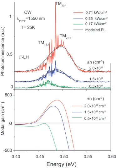
The PL spectra of a 9 µm diameter disk taken at excitation powers below the lasing threshold are shown in Figure3a. Assuming a constant temperature of 25 K, spontaneous emission spectra were calculated for different carrier densities in order to reproduce the broadening of the emission and its blue shift when the pump power increases. The emission blue shift, observed experimentally when increasing the pump power, can be attributed to band filling effect inducing transitions at higher energies, since additional optical transitions occur at higher energies. Considering a band-gap of 465 meV the broadened PL spectra are well reproduced for carrier densities of 0.5 × 1017cm−3, 1.5 × 1017cm−3and 2 × 1017cm−3, which correspond to pump intensities of 0.17 kW cm−2, 0.35 kW cm−2and 0.71 kW cm−2, respectively.
Under cw pumping, the steady state carrier density can be directly linked to the carrier lifetime, using the generation-recombination balance law N = Iτ/(hνd), where I is the absorbed power density, τ the non-radiative generation-recombination lifetime, hν the pump photon energy and d the absorption depth. To obtain the absorbed power used for calculating carrier density and material gain, the incident power is multiplied by 0.65 to account for the disk surface reflectivity at 1550 nm wavelength. The extracted non-radiative lifetimes are 1.4 ns, 2.1 ns and 1.4 ns for carrier densities of 0.5 × 1017cm−3, 1.5 × 1017cm−3and
Photoluminescence (a.u.) T= 25K 0.17 kW/cm2 0.35 kW/cm2 ∆n (cm-3) 2.0x10¹⁷ 1.5x10¹⁷ 0.5x10¹⁷ 0.71 kW/cm2 CW Γ-LH 0.40 0.45 0.50 0.55 0.60 -500 500 Modal gain (cm -1)
Energy (eV)
∆n (cm-3) 0.5x1017 cm-3 1.5x1017 cm-3 2.0x1017 cm-3 0 0.5 1 0 modeled PL λpump=1550 nm TM20,1 TM21,1 TM19,1Figure 3. Carrier density at threshold and net gain (a) PL spectra below threshold, taken at 25 K under cw pumping of
0.2 mW, 0.4 mW and 0.8 mW. WGMs form on top of the spontaneous emission-dominated spectrum. The solid black lines are the calculated spontaneous emission spectra for different carrier densities.(b) Calculated modal gain for the carrier density values from (a).
2 × 1017cm−3, respectively. The obtained values, averaged to around 1.6 ns, are equivalent to those reported in Ref.3. However, even with comparable lifetimes, a clearly lower pumping threshold is here observed. This remarkable feature will be discussed in the next section.
The modal gain illustrated in Figure3b was calculated for the carrier densities mentioned above, assuming steady-state conditions. The required parameters were obtained from the k·p band structure description, and are summarized in Methods. At a carrier density of 0.5 × 1017cm−3the positive gain regime is not reached, but the gain steeply increases with the carrier density. The modal gain maximum is observed at the lasing mode energy of 485 meV. Furthermore, gain broadening is observed for larger pumping intensity due to band filling effects. Note that the calculated modal gain might be overestimated, since it depends on unknown parameters such as homogeneous broadening. Nonetheless, these calculations indicate that modal gain can reach up to 400 cm−1for carrier densities of 2 × 1017cm−3.
Narrow whispering gallery modes appear in addition to the broad spectrum of spontaneous emission, clearly visible in Figure3a. The modes at 472 meV, 485 meV and 497 meV are regularly spaced by 12–13 meV and can be assigned to fundamental TM19,1 TM20,1and TM21,1modes, respectively. Other mode patterns in the spectrum can be attributed to higher radial index modes, with n = 2 and n = 3. The TM19,1mode is close to the band-gap, just a few meV apart. According to gain modelling it does not match the gain maximum. The TM20,1mode, at higher energy, here shows a better match. Thus the TM20,1mode will dominate the spectrum at high powers. This mode competition behaviour leads to a clear single-mode laser emission.
0 25 50 75 100 0 1 2 3 4 5 Threshold (mW) Temperature (K) 800 Wcm-2
(c)
0.45 0.50 0.55 120 K 85 K 65 K 45 K Intensity (a.u.) Energy (eV) x200 25 K 0 25 50 75 100 125 1 10Integrated Intensity (a.u.)
Temperature (K) Emode= 497 meV Ppeak = 11 mW tpulse = 3.5 ns νpulse = 25 MHz
(a)
20 0 40 60 80 5 0 10 15 20 25 30Integrated intensity (a.u.)
Pulse peak power (mW)
(b)
65 K 85 K 120 K 25 K 0 2 4 6 8 1 0 2 3Integrated intensity (a.u.)
65 K
85 K
25 K
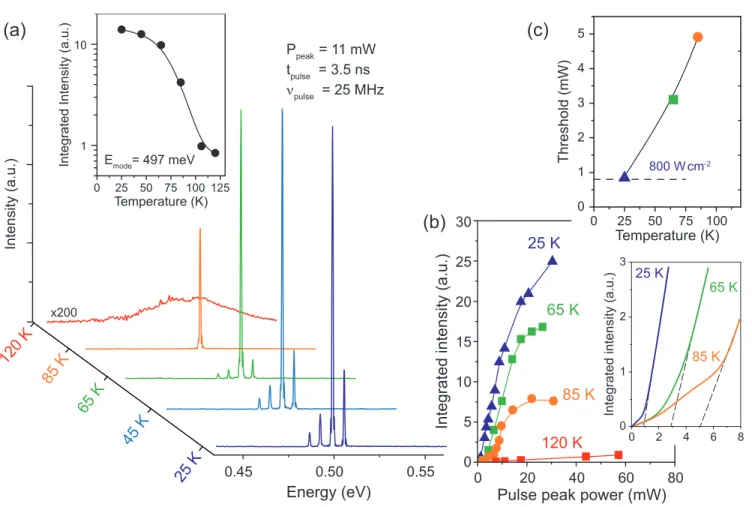
Figure 4. Pulsed laser. a Temperature dependence of light emission of a 9 µm diameter disk under pulsed peak power
excitation of 11 mW. The inset shows the integrated PL signal for the laser mode at 497 meV. b L-L curves at 25 K, 65 K, 80 K and 120 K. No lasing is observed at 120 K. (inset) Zoomed view of L-L curves around threshold. c Lasing threshold as a function of temperature.
Pulsed device results
Since all the GeSn lasers reported in the literature were only operational under pulsed laser excitation, we also studied the properties of the present tensile strained GeSn microdisks. This enables a comparison of GeSn lasers with moderate Sn contents and tensile strain to those reported previously in the literature, having high Sn contents and residual compressive strain. Laser emission spectra taken at temperatures in the range of 25–120 K are shown in Figure4a. 3.5 ns long pulsed excitation at a fixed peak pump power of 11 mW (1 mW average pump power) was here applied. Distinct differences from the cw excitation regime are observed. The laser spectra are multi-mode, with a dominant mode at 497 meV corresponding to a 2.49 µm emission wavelength. Mode assignment can be made by referencing to the spectra shown in Figure3a. The lasing mode at the lowest energy corresponds to the one under cw operation at 485 meV. The dominant mode at 497 meV is also observed at the same energy in Figure3a. From modelling of the whispering gallery modes, we can assign this mode to the transverse magnetic TM21,1, as the free spectral range matches the expectation from modelling. The other two modes, at 488 meV and 502 meV, are assigned to modes with a higher order radial index, i.e. TM17,2and TM18,2. The modes with radial number n = 1 are essentially un-shifted compared to those observed in cw regime in Figure3a. Under pulsed excitation, there is a non-uniform spatial distribution of carriers, and possibly also a non-equilibrium distribution over the conduction band valleys, as well as a different temperature gradient compared to cw excitation. The non-uniform/non-equilibrium distribution explains the shift of gain to modes with higher radial order indices. In the pulsed regime, the gain profile may indeed be different from that in cw, enabling multi-mode lasing and favouring higher energy modes. At higher temperatures, the laser spectra become single-mode (Figure4a), indicating a narrower frequency range of positive gain. However, more importantly, the maximum laser operation temperature in pulsed operation is almost two times higher than in cw regime.
The L-L characteristics for different temperatures are given in Figure4b. Here, a thermal roll-over occurs at 85 K for 20 mW peak pumping power (1.8 mW average power), compared to 5 mW at 25 K under cw excitation. For pulsed operation at 25 K
a lasing threshold peak power of 0.9 mW is measured (inset of Figure4b), which corresponds to a record low pump power density of 0.8 kW cm−2. This pump power density is 250 times smaller than that of the best bulk GeSn microdisk laser reported in the literature. The threshold is temperature dependent, as shown in Figure4c. A rise in temperature to 85 K increases the threshold power density to 4.2 kW cm−2. At 120 K no lasing signature is observed anymore. The maximum temperature at which the gain should be still detectable depends on the carriers density as well. Simulations of the gain for an electron / hole density of 1 × 1017cm−3indicate that the gain in this material becomes quite small at 120 K. Taking parasitic losses like scattering on surface roughness into account, these simulation results match the experimental observation.
In this paragraph we qualitatively discuss the laser operation mode, maximum lasing temperature and threshold pump power density for GeSn layers under tensile strain, and benchmark the results against literature data.
In our experiment, where pumping is above the lasing threshold, the steady-state carrier density is expected to be nearly constant since the quasi- Fermi level is clamped by stimulated emission process. Although all electrons are generated in the Γ-valley, many of them will scatter into the L-valley. In particular, for a small ∆EL−Γ, here only 70 meV, and an energy difference between the quasi Fermi level and the L-valley of only 40 meV, estimated at 25K for an electron-hole density of 2 × 1017cm−3, a substantial amount of carriers will cool down/scatter into the L-valley. The intra- and inter-valley carrier scattering times, by phonon emission/absorption, are in the ps range while the thermal relaxation time for the disk is in the µs range. This implies an equilibrium carrier distribution in cw, at a lattice temperature above the nominal temperature, by about 20–30 K under 8 mW pump power (see SI). The scattering rates increase with temperature and with the decrease of ∆EL−Γ, increasing the carrier density in the L-valleys superlinearly with the pump power. This leads to a decrease of the gain since carriers in L-valleys only contribute to free carrier absorption without any contribution to gain. Moreover, as the temperature is increased, the carrier density is affected by increased non-radiative recombinations that decreases the overall gain (see SI). Consequently, a roll-over of the L-L spectrum at 25 K is observed for an excitation power exceeding 7 mW and, above 45 K, lasing is strongly quenched. These results hint to a heating of the electron bath by 40 K above the nominal sample temperature. It was experimentally observed that reducing the pump photon energy, and consequently reducing the lattice heating, leads to increased maximum operating temperatures by about 20 K12,17. The role of the lattice heating is underlined by the experimental observation of operation temperature increase by almost 30 K for the 12 µm disks. The heat dispersion by the Al pillar is then better than for 9 µm disks.
Operating the same laser under pulsed excitation substantially reduces the thermal load, improving the temperature performance of the device. Laser quenching appears above 85 K for 9 µm disks and 100 K for 12 µm disks. The operation temperature increase for pulsed operation is only 15 K, about a half of that for cw operation. This indicates that cw lasing is much more sensitive to temperature than the pulsed operation. This may explain why no cw lasing was observed in compressively strained GeSn laser where the pumping powers were 100-200 times larger than in this work. Multi-mode and single-mode lasing for pulsed and cw pumping, respectively, is likely related to an incomplete wash-out of spatial hole-burning by carrier diffusion, together with a larger gain, for pulsed pumping37.
Next we compare the results with those for Ge0.875Sn0.125microdisk laser with residual compressive strain, with a similar diameter of 8 µm4, emitting at almost the same energy of ∼0.5 eV (2.5 µm), having similar band-gap and directness ∆EL−Γ. With much stronger pump pulses, but 3 orders of magnitude smaller duty cycle, the average pump power and heat load there were lower, so it could tolerate a larger gain drop with increasing temperature, enabling a larger maximum operating temperature, of ∼130 K. The laser active layer in this work is the thinnest reported to date, less than a half of that in Ref.4 (260 nm vs. 560 nm), hence the mode overlap factors (affecting modal gain) also differ, being just 17 % here and 95 % in Ref.4. Even so, the GeSn device strained by SiNxlayers shows substantially lower threshold.
The main achievement of the presented GeSn laser is that it enables cw operation. This is a direct consequence of the strongly reduced threshold power, by at least a factor of 250 , which allows continuous pumping while maintaining a moderate lattice temperature. This drastic improvement is attributed to three factors: (i) The large reduction of the valence band DOS (∆ELH−HH = 172 meV), warrants that the population inversion is achieved at a lower density of excited carriers. (ii) The modal gain of tensile strained GeSn is improved compared to unstrained GeSn with higher Sn content and the same ∆EL−Γ14. (iii) The non-radiative recombination rate is substantially reduced in lower Sn content alloys and even more so in the present structure with the defective epitaxial interface intentionally removed during processing. Defect reduction engineering is crucial, as previously reported for GeSn/SiGeSn quantum wells (QWs) lasers17.
The above discussion should provide some guidelines for improving the laser performance, by combining the advantages of the present structure with those from the previous GeSn laser research. An increase of the operating temperature up to 230 K was obtained by increasing the Sn content to 16 at. %7, and hence the directness ∆EL−Γ. Tensile strain can considerably reduce the requirement for high Sn contents. A tensile strain of 1.5 % in 10 at. % Sn alloy results in a very large Γ population at 300 K (see SI), and is, therefore, a viable route towards application-ready GeSn lasers. In addition, the use of SiGeSn/GeSn QWs heterostructures brings additional benefits from carrier confinement and energy quantization, enabling a threshold reduction by almost an order of magnitude for strain relaxed SiGeSn/GeSn QW17. Heterostructures as in Ref.38, combined with tensile
strain, would strongly improve the carrier confinement at higher temperatures and, consequently, further decrease the threshold pump power density. QWs heterostructures yield a separation of the active region from interface defects without the use of a layer transfer technology, which is desirable for low-cost, high yield fabrication. In the present work bonding was used as a straightforward way to identify the intrinsic material optical properties. For tensile strain engineering, however, layer transfer is also not a mandatory solution, since several previous works have shown the feasibility of using a single stressor in cavities within a fully monolithic approach25,26,39. Finally, the use of stessor layers has been shown to be compatible with an electrical pumping scheme40that could be incorporated into the presently used layout.
Conclusion
In summary, we have demonstrated a GeSn-based laser fully embedded in a SiNx stressor conform layer. Starting with an indirect band-gap GeSn alloy we converted it, by inducing tensile strain, into a direct-gap optical gain material. Most importantly, cw and pulsed laser operation with ultra-low lasing thresholds of 0.8–1.1 kW cm−2are demonstrated. These values are significantly lower than any value reported for group-IV lasers, and are even comparable to those for epitaxially grown III-V InP lasers41, or InGaAs lasers bonded on Si wafers42, albeit the latter operate at room temperature. This achievement relies on using dilute GeSn alloys with just 5.4 at. % Sn, in contrast to the mainstream research focusing on 16–20 at. % Sn. While the lower Sn content decreases the ∆EL−Γsplitting (directness), tensile strain compensates for that and, additionally, offers a reduced DOS by shifting the LH band above the HH band. In the present work, we combine the material quality advantage of low Sn content alloys and the physics of tensile strain with processing technology and thermal management, enabling lasing in low Sn-content alloys at record-low pumping powers and operating in a cw regime. Consequently, a viable route towards room temperature operation is predicted by combining modest Sn concentrations of ∼10% with tensile strain >1% in the active layer.
Methods
Optical PL excitation was provided by an Nd:YAG laser at 1064 nm wavelength focused on the sample surface with a mi-croscope objective, ×40 and Numerical Aperture (NA) of 0.65, into a 5 µm diameter spot. Collection of emitted light was performed with the same microscope objective, and a beamsplitter was used to separate emission and excitation beam paths. In these experiments, we used an extended InGaAs detector to detect the luminescence. The high sensitivity, enabling the detection of low levels of infrared signals, was counterbalanced by the 2.5 µm wavelength cut-off due to the detector and objective transmission quenching.
Lasing experiments were performed using a µ-PL setup, where the cw pump laser beam at 1550 nm wavelength was fo-cused on the sample surface into a 12 µm spot diameter by a x40 reflective objective with NA of 0.5 and working distance of 4 mm. The same objective was used for pumping and for collection of light emitted from the microdisk. A CaF2beamsplitter was used to separate the excitation and emission beam paths. The outgoing emission, collected from the objective, was coupled to a Fourier Transform Infrared (FTIR) spectrometer equipped with a CaF2beam splitter. The emission was detected by a nitrogen-cooled InSb photodetector, which has a cut-off wavelength 4.8 µm. The telecom wavelength pump laser was out-coupled from a single-mode fiber to free space using a hyperbolic mirror, the output fiber being clamped at the focal point of the mirror. The pump can be taken through a Mach-Zehnder modulator, controlled by an rf-pulse generator so that the pump beam power can be switched from cw to quasi-continuous and to pulsed mode. The same output from a single-mode fiber was used in both cases, cw or pulsed, so that switching from one pump mode to another did not induce any change of the beam waist or its alignment to the disk. The pulse shape under modulated excitation had 3.5 ns width and a repetition rate of 25 MHz. As discussed below, the pulse duration was longer than the non-radiative lifetime, so the optical excitation can be considered quasi-cw in this respect. The FTIR spectrometer resolution was set to 0.25 cm−1for line-width narrowing analysis of lasing mode around threshold otherwise it was set to 4 cm−1.
Calculation of whispering gallery modes was performed by a 2D analytical model. The resonance wavelength of the cavity mode with azimuthal index m is calculated from the roots of mthBessel function Im(2πne f f
(λ )
λres a). The optical field is plotted at
the resonant wavelength to obtain the corresponding radial number n of nodes along the disk radius. To account for modal dispersion of vertically confined modes, the effective index is introduced in the model, according to ne f f(λ ) = −0.6λ + 3.85, where λ is the wavelength in µm. This expression was interpolated from 1D slab modelling of TM polarized waves, propagating in the GeSn layer. The energy of the TM20,1mode is calculated to be 484.65 meV, in good agreement with the 485 meV experimental value.
Optical gain is calculated within the framework of parabolic band effective mass model, using the equation28 g(¯hω) = DTMΓ,LH 2 ∞ Z 0
ρLH(E)( fC(E) − fV(E))
Γ0
2π (Γ0
2)2+ (EΓ,LH+ E − ¯hω)2 dE,
where ρLH(E) is the joint density of states involving the Γ conduction band and the LH valence band, and D TM Γ,LH 2 is the interband dipole matrix element. Γ0is the full width at half maximum of a Lorentzian function, which is here set to 25 meV to account for homogeneous broadening of interband transitions, while fC(E) and fV(E) are the Fermi-Dirac functions for electrons and holes. The density of states effective masses, used in the calculation, were mΓ= 0.036 m0, mL= 0.56 m0, and mLH= 0.05 m0, extracted from the k.p model14of strained GeSn with 5.4 at. % Sn content and biaxial tensile strain of 1.4 %. The energy splitting ∆EL−Γ= EL− EΓ, ∆ELH−HH = ELH− EHHand the band-gap EΓ− ELHamount to 70 meV, 170 meV and 465 meV, respectively, according to k.p modeling and PL results. Note that the density of states effective masses differ only slightly from those in pure Ge, and we have therefore used the free carrier absorption model for pure Ge, assuming it would be very close to that for low Sn content GeSn alloy, in order to deduct it from the interband gain and find the net gain.
Acknowledgements
M.E.K. and A.E. thank Dr. Raffaele Colombelli and Prof. Adel Bousseksou for fruitful discussions and their help in mounting the PL setup with the FTIR spectrometer. The authors thank Dr. Gregor Mussler for XRD measurements. This work used knowledge acquired in the collaboration with Dr. Hans Sigg from PSI. This work was supported by the French RENATECH network, the French national research agency (Agence Nationale de la Recherche - ANR) through funding of ELEGANTE project (ANR-17-CE24-0015) and the Deutsche Forschungsgemeinschaft (DFG) via the project “SiGeSn Laser for Silicon Photonics”. A.E. was supported by ANRT through a CIFRE grant. A. F. gratefully acknowledges funding within the ANR-16-CE09-0029-03 TIPTOP project.
Author contributions statement
All authors contributed to the work. P.B. M.E.K. and A.E. designed the device structure. M.E.K. and A.E. performed the strained disks fabrication with E.H., I.S., K.P., and G.P.. M.E.K. and A.E. performed the PL measurements and laser experiments with N.Z. and X.C.. K.P., G.P., I.S., N.v.d.D. and D.B. performed the structural analysis of the material. The GeSn layer was grown by D.B. and N.v.d.D. on substrates from J.-M.H.. The Raman analyses were performed by A.F. and R.O.. P.B., S.S. and Z.I. contributed to the modelling with M.E.K. and D.B.. The work was supervised by D.G., F.B., P.B., D.B. and M.E.K.. P.B, M.E.K., N.v.d.D., D.G and D.B. wrote the manuscript.
Competing interest
The authors declare no competing financial interests.
Data availability statement
The data that support the plots within this paper and other findings of this study are available from the corresponding author upon reasonable request.
Code availability statement
Finite element modeling was performed using a commercially available COMSOL software. All-other calculation codes were used in published works where model details are provided. The codes are not publicly available, any requests should be sent to the corresponding authors.
References
1. Soref, R. A., Buca, D. & Yu, S.-Q. Group IV Photonics - Driving Integrated Optoelectronics. Opt. & Photonics News 27, 32–39, DOI:10.1364/OPN.27.1.000032(2016).
3. Wirths, S. et al. Lasing in direct-bandgap GeSn alloy grown on Si. Nat. Photonics 9, 88–92, DOI:10.1038/nphoton.2014. 321(2015).
4. Stange, D. et al. Optically Pumped GeSn Microdisk Lasers on Si. ACS Photonics 3, 1279–1285, DOI:10.1021/ acsphotonics.6b00258(2016).
5. Reboud, V. et al. Optically pumped GeSn micro-disks with 16% Sn lasing at 3.1 µm up to 180 K. Appl. Phys. Lett. 111, 092101, DOI:10.1063/1.5000353(2017).
6. Al-Kabi, S. et al. An optically pumped 2.5 µm GeSn laser on Si operating at 110K. Appl. Phys. Lett. 109, 171105, DOI:
10.1063/1.4966141(2016).
7. Thai, Q. M. et al. GeSn heterostructure micro-disk laser operating at 230K. Opt. Express 26, 32500–32508, DOI:
10.1364/OE.26.032500(2018).
8. Hodgkinson, J. & Tatam, R. P. Optical gas sensing: a review. Meas. Sci. Technol. 24, 012004, DOI:10.1088/0957-0233/ 24/1/012004(2013).
9. Sieger, M. & Mizaikoff, B. Toward On-Chip Mid-Infrared Sensors. Anal. Chem. 88, 5562–5573, DOI:10.1021/acs. analchem.5b04143(2016).
10. Singh, V. et al. Mid-infrared materials and devices on a Si platform for optical sensing. Sci. Technol. Adv. Mater. 15, 014603, DOI:10.1088/1468-6996/15/1/014603(2014).
11. Razeghi, M. & Nguyen, B.-M. Advances in mid-infrared detection and imaging: a key issues review. Reports on Prog. Phys. 77, 82401, DOI:10.1088/0034-4885/77/8/082401(2014).
12. Dou, W. et al. Optically pumped lasing at 3 µm from compositionally graded gesn with tin up to 22.3%. Opt. Lett. 43, 4558, DOI:10.1364/OL.43.004558(2018).
13. Zhou, Y. et al. Optically pumped gesn lasers operating at 270 k with broad waveguide structures on si. ACS Photonics 6, 1434–1441, DOI:10.1021/acsphotonics.9b00030(2019).https://doi.org/10.1021/acsphotonics.9b00030.
14. Rainko, D. et al. Impact of tensile strain on low Sn content GeSn lasing. Sci. Reports 9, 259, DOI: 10.1038/ s41598-018-36837-8(2019).
15. Gencarelli, F. et al. Crystalline properties and strain relaxation mechanism of CVD grown GeSn. ECS Transactions 50, 875–883, DOI:10.1149/05009.0875ecst(2013).
16. Dou, W. et al. Investigation of GeSn Strain Relaxation and Spontaneous Composition Gradient for Low-Defect and High-Sn Alloy Growth. Sci. Reports 8, 5640, DOI:10.1038/s41598-018-24018-6(2018).
17. Stange, D. et al. GeSn/SiGeSn heterostructure and multi Quantum Well Lasers. ACS Photonics 5, 4628–4636, DOI:
10.1021/acsphotonics.8b01116(2018).https://doi.org/10.1021/acsphotonics.8b01116.
18. Du, W. et al. Study of si-based gesn optically pumped lasers with micro-disk and ridge waveguide structures. Front. Phys. 7, 147, DOI:10.3389/fphy.2019.00147(2019).
19. Minamisawa, R. et al. Top-down fabricated silicon nanowires under tensile elastic strain up to 4.5%. Nat. Commun. 3, 1096, DOI:10.1038/ncomms2102(2012).
20. El Kurdi, M. et al. Direct Band Gap Germanium Microdisks Obtained with Silicon Nitride Stressor Layers. ACS Photonics 3, 443–448, DOI:10.1021/acsphotonics.5b00632(2016).
21. Virgilio, M., Manganelli, C. L., Grosso, G., Pizzi, G. & Capellini, G. Radiative recombination and optical gain spectra in biaxially strained n-type germanium. Phys. Rev. B 87, DOI:10.1103/physrevb.87.235313(2013).
22. Bao, S. et al. Low-threshold optically pumped lasing in highly strained germanium nanowires. Nat. Commun. 8, 1845, DOI:10.1038/s41467-017-02026-w(2017).1708.04568.
23. Süess, M. J. et al. Analysis of enhanced light emission from highly strained germanium microbridges. Nat. Photonics 7, 466–472, DOI:10.1038/nphoton.2013.67(2013).
24. Armand Pilon, F. T. et al. Lasing in strained germanium microbridges. Nat. Commun. 10, 2724, DOI: 10.1038/ s41467-019-10655-6(2019).
25. Ghrib, A. et al. Control of tensile strain in germanium waveguides through silicon nitride layers. Appl. Phys. Lett. 100, 201104, DOI:10.1063/1.4718525(2012).
26. Capellini, G. et al. Strain analysis in SiN/Ge microstructures obtained via Si-complementary metal oxide semiconductor compatible approach. J. Appl. Phys. 113, 013513, DOI:10.1063/1.4772781(2013).
27. von den Driesch, N. et al. Direct bandgap group IV epitaxy on Si for laser applications. Chem. Mater. 27, 4693–4702, DOI:10.1021/acs.chemmater.5b01327(2015).
28. Ghrib, A. et al. All-Around SiN Stressor for High and Homogeneous Tensile Strain in Germanium Microdisk Cavities. Adv. Opt. Mater. 3, 353–358, DOI:10.1002/adom.201400369(2015).
29. Zaumseil, P. et al. The thermal stability of epitaxial gesn layers. Appl. Phys. Lett. Mater. 6, 076108, DOI:10.1063/1. 5036728(2018).
30. Elbaz, A. et al. Solving thermal issues in tensile-strained Ge microdisks. Opt. Express 26, 28376–28384, DOI:10.1364/ OE.26.028376(2018).
31. Elbaz, A. et al. Germanium microlasers on metallic pedestals. APL Photonics 3, 106102, DOI:10.1063/1.5025705(2018). 32. Uchida, N. et al. Carrier and heat transport properties of polycrystalline gesn films on sio2. Appl. Phys. Lett. 10, 232105,
DOI:10.1063/1.4937386(2015).
33. Pezzoli, F., Giorgioni, A., Patchett, D. & Myronov, M. Temperature-dependent photoluminescence characteristics of GeSn epitaxial layers. ACS Photonics 3, 2004–2009, DOI:10.1021/acsphotonics.6b00438(2016).
34. Cheng, R. et al. Relaxed and strained patterned germanium-tin structures: A raman scattering study. ECS J. Solid State Sci. Technol. 2, P138–P145, DOI:10.1149/2.013304jss(2013).
35. Rabolt, J. F. & Bellar, R. The nature of apodization in fourier transform spectroscopy. Appl. Spectrosc. 35, 132–135, DOI:
10.1366/0003702814731987(1981).
36. El Kurdi, M. et al. Tensile-strained germanium microdisks with circular Bragg reflectors. Appl. Phys. Lett. 108, 091103, DOI:10.1063/1.4942891(2016).
37. Sargent, M. Theory of a multimode quasiequilibrium semiconductor laser. Phys. Rev. A 48, 717–726, DOI:10.1103/ PhysRevA.48.717(1993).
38. Stange, D. et al. Short-wave infrared leds from gesn/sigesn multiple quantum wells. Opt. 4, 185–188, DOI:10.1364/ OPTICA.4.000185(2017).
39. Ghrib, A. et al. Tensile-strained germanium microdisks. Appl. Phys. Lett. 102, 221112, DOI:10.1063/1.4809832(2013). 40. Prost, M. et al. Tensile-strained germanium microdisk electroluminescence. Opt. Express 23, 6722–6730, DOI:10.1364/
OE.23.006722(2015).
41. Wang, Z. et al. Novel Light Source Integration Approaches for Silicon Photonics. Laser & Photonics Rev. 11, 1700063, DOI:10.1002/lpor.201700063(2017).1610.06300.
42. Seifried, M. et al. Monolithically Integrated CMOS-Compatible III–V on Silicon Lasers. IEEE J. Sel. Top. Quantum Electron. 24, 1–9, DOI:10.1109/JSTQE.2018.2832654(2018).
a
280
290
300
Ge reference
as-grown GeSn
bonded GeSn
all-around
SiN stressor
Raman signal intensity (a.u.)
310
k
E
HH
LH
L-valley
Γ
-valley
720 meV
660 meV
as-grown
20 K, -0.32%
-30 meV
k
E
HH
LH
L-valley
Γ
-valley
466 meV
535 meV
final laser device
80 K, 1.40 %
170 meV
e
f
tensile
strain
GeSn layer
bonding &
substrate removal
c
b
micro disk
structuring
&
SiN deposition
GeSn
Ge-VS
as-grown
a
out-of-plane(Å)
Ge-VS
GeSn
5.60
5.65
5.70
5.75
5.60
5.65
5.70
5.75
a
in-plane(Å)
pseudomorphic line
strain-relaxed line
Photoluminescence (a.u.)
0.4
0.5
0.6
0.7
0.8
bonded
x10
d
Γ-HH
Sim
80 K
8 mW
LN InSb
Γ
-LH
as-grown
x10
20 K
15 mW
InGaAs
L-HH
all-around
SiN
2 µm
Al
SiN
GeSn
2 µm
10 nm
T = 25 K λpump = 1.55 µm dDisk = 9
µ
m x25 x100 x100 x200 0.2 0.4 0.8 1.3 1.9 3.2 cw pump power (mW)TM
20,1a
480 484 488 10-4 10-3 10-2 10-1 1 PL Intensity (a.u.) Energy (meV) λ = 2.56 µm Ppump= 2.3 mWb
FWHM (µeV) 1 2 3 101 102 103 104Peak Intensity (a.u.)
cw power (mW) 60 80 100 120 40 100
c
details at thresholde
0.475 0.45 0.50 0.525 0.55 30 K 80 K 72 K 61 K 50 K 40 K Energy (eV) dDisk = 12µ
m Ppump = 10 mW 0 10 20 30 40 65 K 45 K 25 KIntegrated intensity (a.u.)
d
25 K 45 K 1.1 kW cm-2 dDisk = 9 µm x10Photoluminescence (a.u.) T= 25K 0.17 kW/cm2 0.35 kW/cm2 ∆n (cm-3) 2.0x10¹⁷ 1.5x10¹⁷ 0.5x10¹⁷ 0.71 kW/cm2 CW Γ-LH 0.40 0.45 0.50 0.55 0.60 -500 500 Modal gain (cm -1) ∆n (cm-3) 0.5x1017 cm-3 1.5x1017 cm-3 2.0x1017 cm-3 0 0.5 1 0 modeled PL λpump=1550 nm TM20,1 TM21,1 TM19,1
0 25 50 75 100 0 1 2 3 4 5 Threshold (mW) Temperature (K) 800 Wcm-2
(c)
0.45 0.50 0.55120 K
85 K
65 K
45 K
Intensity (a.u.) x20025 K
0 25 50 75 100 125 1 10Integrated Intensity (a.u.)
Temperature (K) Emode= 497 meV Ppeak = 11 mW tpulse = 3.5 ns νpulse = 25 MHz
(a)
20 0 40 60 80 5 0 10 15 20 25 30Integrated intensity (a.u.)
(b)
65 K
85 K
120 K
25 K
0 2 4 6 8 1 0 2 3Integrated intensity (a.u.)
65 K
85 K