Development of an Immersion Maskless
Lithography System
by
David Chao
B.S. Electrical Engineering, Cornell University (2003)
Submitted to the Department of
Electrical Engineering and Computer Science
in partial fulfillment of the requirements for the degree of
Master of Science
at the
MASSACHUSETTS INSTITUTE OF TECHNOLOGY
MIASSACHUSETTS INSTrTUE] OF TECHNOLOGY
MAR
28.2006
LIBRARIES
September 2005
© Massachusetts Institute of Technology 2005. All rights reserved.
Author ...
...
...
Department of Electrical Engineering and Computer Science
September 6, 2005
Certified by ...
.
.
.
Henry I. Smith
eithiey Professor of Electrical Engineering
Thesj<Supervisor
Accepted by ...
...
Arthur
C. Smith
Chairman, Department Committee of Graduate Students
Development of an Immersion Maskless
Lithography System
by
David Chao
Submitted to the Department of Electrical Engineering and Computer Science on September 6, 2005, in partial fulfillment of the requirements for the degree of
Master of Science
Abstract
As lithography quickly approaches its limits with current technologies, a host of new ideas is being proposed in hopes of pushing lithography to new levels of performance. The work presented in this thesis explores the use of an immersion scheme to improve the performance of a maskless lithographic technique known as Zone-Plate-Array Lithography (ZPAL). This is believed to be the first implementation of an immersion scheme in a maskless lithography system.
This thesis provides a complete description of the Immersion Zone-Plate-Array Lithography (iZPAL) system. Since the zone plate component of the system is largely responsible for its lithographic performance, a thorough analysis of zone plate theory, design, and fabrication is also presented. The focusing performance of an immersion zone plate is then characterized through the experimental reconstruction of its point-spread function. Finally, lithography results obtained with the iZPAL system are compared to those obtained with the non-immersion ZPAL system, demonstrating the improvement in resolution, exposure latitude, and depth-of-focus achieved with the immersion scheme.
Thesis Supervisor: Henry I. Smith
Title: Keithley Professor of Electrical Engineering
-Acknowledgements
Seasons come and go, experiments succeed and fail, theories stand and fall apart, but the one thing that has remained constant throughout my two years at MIT has been the group of people I have learned to rely on - the very people responsible for my success.
At the core of this group is Professor Henry Smith. His contagious passion and optimism made even the most daunting of goals appear attainable and worth striving for. He set goals, but gave me tremendous freedom to design my own course of research to meet these goals. This has not only made me a better scientist, it has made me a stronger and more responsible person. The considerable number of distinguished scholars who have once worked and learned under his direction is a testament to him as an advisor. Thank you for giving me the opportunity to be a part of this wonderful team that is the NSL.
Throughout my involvement with ZPAL, I have always thought of Rajesh Menon as a shining example of what it means to be a good researcher. He, more than anyone, has shown me that hard work and dedication are the keys to success. Thank you for being a great role model and for exceeding my expectations as a mentor.
Speaking of exceeding expectations, I've learned that a good officemate does more than just keep his half of the space tidy. Every time I ran into an obstacle, I could always count on Amil Patel, Officemate Version 1.0 and fellow ZPAL teammate, to help as best he could. He would always take my questions seriously, even the 'dumb' ones. And he was always up for a debate, especially when it came to football. Thank you for being a great colleague and friend.
When it came to fabrication, no one was more helpful than Tymon Barwicz. I would probably still be stuck in the early phases of this project if it were not for many of his wonderful insights. Thank you for sharing your knowledge with me. I would also like to thank Feng Zhang for the countless number of times he helped me troubleshoot the Raith 150, even during weird hours of the night.
The lab can be a very frustrating place most days. Fortunately, Jim Daley is always around to cheer everyone up. It is remarkable how he manages to keep the lab running so smoothly in addition to assisting anyone (and everyone) in need of help.
-5-Thank you for being so generous with your valuable time. -5-Thanks also to Minghao Qi for keeping me company (and sane) during those many late nights that became early mornings.
I would also like to acknowledge the U.S. Department of Defense for supporting me this past year through the National Defense Science and Engineering Graduate Fellowship.
Success takes the right amount of determination, support, and even a little luck. Thank you fellow NSLers for contributing to my success in so many ways. Thank you also to the rest of my friends for helping me not lose sight of life outside the lab. Thank you to the Wong family for always being enthusiastic about my work and for showing a genuine concern for my well-being. Thank you to my parents and sister for your constant support and encouragement. Even when I questioned my own decisions, you were always there to give me reassurance.
And finally, these acknowledgements would not be complete without thanking my best friend and partner in life, Karen. Thank you for putting up with me and all of my annoying tendencies. Thank you for taking care of everything when I was consumed with work, and even when I wasn't. Thank you for loving me.
Contents
Chapter 1: Introduction - Immersion Maskless Lithography ... 13
1.1 Mask-Based Lithography vs. Maskless Lithography...14
1.1.1 Maskless Technologies ... 17
1.1.1.1 Electron-Beam Lithography (SST)...18
1.1.1.2 ASML/Micronic's Maskless Lithography System (VMT)...19
1.2 Immersion Lithography ... 20
1.2.1 An Immersion Optical Projection Lithography System...23
1.3 The 1st Immersion Maskless Lithography System... 24
Chapter 2: Immersion Zone-Plate-Array Lithography: System Description and Experimental Operation ... 25
2.1 Zone-Plate-Array Lithography (ZPAL)... 25
2.2 ZPAL's Key Components...27
2.2.1 The Radiation Source... 27
2.2.2 The Spatial Light Modulator... 27
2.2.3 The Zone-Plate Array ... 31
2.2.3.1 Diffractive vs. Refractive Lens Technologies ... 32
2.2.4 The Scanning Stage...33
2.2.5 The Control Computer ... 33
2.3 Transforming ZPAL into iZPAL ... 34
2.4 Experimental Setup Procedure... 35
2.4.1 Parallelization ... 36
2.4.2 G apping ... 37
-7-Chapter 3: Zone Plates: Theory, Design, and Fabrication ... 39
3.1 Zone Plate Theory... 40
3.2 Zone Plate Design... 43
3.2.1 Computing ri, ... , rn:... 43
3.2.2 Remaining Zone Plate Design Steps... 44
3.2.3 Amplitude vs. Phase Zone Plates...45
3.3 M ore Zone Plate Theory: Fourier Analysis ... 47
3.3.1 Amplitude Zone Plates...47
3.3.2 Phase Zone Plates ... 50
3.4 Zone Plate Fabrication... 51
3.4.1 The Non-Immersion Zone Plate Fabrication Process ... 52
3.4.2 The Immersion Zone Plate Fabrication Process ... 55
3.4.2.1 Reflection Analysis... 55
3.4.2.2 Fabrication Process ... 57
Chapter 4: Zone Plate Characterization... 61
4.1 The Analytical Approach... 62
4.2 The Experimental Approach... 64
4.3 Characterization of Immersion Zone Plates... 68
Chapter 5: iZPAL System Performance...71
5.1 Resolution ... 72
5.2 Exposure Latitude and Depth-of-Focus (DOF) ... 75
5.3 Additional Lithography Results... 77
Chapter 6: Conclusion - Future W ork... 81
6.1 A Potential Solution to an Earlier Problem... 82
6.2 Future Immersion Experiments... 84
List of Figures
Fig. 1-1 Schematic of an optical projection lithography system...14
Fig. 1-2 Depiction of a maskless lithographic printing technique...15
Fig. 1-3 Schematic of an electron beam lithography system...16
Fig. 1-4 ASML/Micronic's Sigma7000 Series maskless lithography system...19
Fig. 1-5 A pictorial illustration of the numerical aperture of an optical system...21
Fig. 1-6 Schematic of an immersion optical projection lithography system...23
Fig. 2-1 Schematic of Zone-Plate-Array Lithography (ZPAL)...26
Fig. 2-2 Photograph of the prototype ZPAL system ... 28
Fig. 2-3 Implementation of the Digital Micromirror Device (DMD) in ZPAL ... 29
Fig. 2-4 Implementation of the Grating Light ValveTM (GLVTM) in ZPAL...30
Fig. 2-5 The refractive process for focusing light ... 32
Fig. 2-6 Schematic of Immersion Zone-Plate-Array Lithography (iZPAL) ... 34
Fig. 2-7 A Mach-Zender interferometer setup similar to the one used to parallelize the zone-plate array to the substrate... 36
Fig. 2-8 The confocal microscopy setup used to gap the zone-plate array to the substrate ... . 38
Fig. 3-1 The am plitude zone plate ... 41
Fig. 3-2 A plot of the real part of the phase component expressed in Eq. 3-1 ... 42
Fig. 3-3 Zone plate geometry, illustrating the relationship between ri, ... , r, and f, k , T ... 4 4 Fig. 3-4 A depiction of the phase shift between light propagating in two different m edium s... . . 46
Fig. 3-5 The transmission function of an amplitude zone plate ... 48
Fig. 3-6 The multiple diffractive orders of an amplitude zone plate...49
-9-Fig. 3-7 The transmission function of a phase zone plate ... 50
Fig. 3-8 The two-step non-immersion zone plate fabrication process ... 52
Fig. 3-9 The purpose of the Cr layer for ZPAL...54
Fig. 3-10 A planar three-layer (two-boundary) structure ... 56
Fig. 3-11 A plot of the total back-reflection from the medium depicted in Figure 3-10, as a function of SiN thickness... 56
Fig. 3-12 The immersion zone plate fabrication process...57
Fig. 3-13 An optical micrograph of immersion zone plates fabricated using the process outlined in Figure 3-12 ... 58
Fig. 3-14 Scanning electron micrographs of a 1.14 NA immersion zone plate, designed for 400nm light ... 59
Fig. 4-1 An approximate point-spread function of a 0.54 NA immersion zone plate com puted w ith Eq. 4-5... 64
Fig. 4-2 Accurate and approximate point-spread functions (PSFs) of a 1.14 NA im m ersion zone plate ... 65
Fig. 4-3 The point-spread function (PSF) reconstruction process...66
Fig. 4-4 Typical nonlinear behavior of positive photoresists ... 67
Fig. 4-5 Comparison between the experimental and theoretical immersion and non-immersion zone plate point-spread functions (PSFs)...68
Fig. 5-1 Dense lines and spaces patterned with ZPAL ... 73
Fig. 5-2 Dense lines and spaces patterned with iZPAL...73
Fig. 5-3 Comparison between 135nm dense lines/spaces patterned with both Z PA L and iZPA L ... 75
Fig. 5-4 Plots of exposed linewidths measured over a range of dose and defocus for both ZPA L and iZPA L ... 76
Fig. 5-5 Exposure w indow plots... 77
Fig. 5-6 Dense nested-L's (150nm and 190nm) patterned with iZPAL ... 78
Fig. 5-7 Dense array of holes (15Onm and 190nm) patterned with iZPAL ... 79
Fig. 5-8 Immersion maskless lithographic patterning of the official logo of the Electron, Ion, and Photon Beam Nanofabrication and Technology (EIPBN) conference 2005 ... 79
Fig. 6-1 An illustration of a potential problem with the current iZPAL experimental setup procedure ... 83 Fig. 6-2 The filling of a zone plate with Cytop ... 84
-Chapter 1
Introduction
-
Immersion Maskless Lithography
Much of the groundbreaking research being conducted today in the fields of telecommunications, computer computation, and biology (just to name a few) can largely attribute their successes to the science known as 'Nanotechnology.' Nanotechnology has enabled much of the life we know today, being responsible for many of life's luxuries as well as necessities - from computers for entertainment, to cellphones for communication, to cutting-edge biotechnology for medical breakthroughs. Can one now imagine life without nanotechnology?
At the foundation of all that is nanotechnology lies lithography, its vehicle for existence (its key enabling agent). Lithography, which literally means 'writing in stone,' is a method of printing. One of its earliest manifestations came in the form of engraving patterns onto stone slabs using oil-tipped utensils. The stone slabs were subsequently wet with water-based ink, and since oil repels water, a thin film of ink was left behind wherever the oil was not present. The stones slabs were now ready to be used as stamps for printing. Today, lithography is performed in a number of ways, the most common of which are based on optical, electron, and imprint techniques. Using optical lithography as an example, light is focused onto a photosensitive material, changing its chemical
-properties. The pattern is subsequently defined in the material through the use of a developing agent, which selectively removes the areas exposed to the focused optical beam. Since light can be focused down to sub-wavelength dimensions, patterns in the nanometer scale can be created using optical lithography.
1.1 Mask-Based Lithography vs. Maskless Lithography
All forms of lithography can be grouped into two categories: mask-based lithography and maskless lithography. In the mask-based case, an image of a mask containing pre-defined patterns (usually produced using a maskless lithographic approach) is projected
Light
_}>
4, 4,4~ ---- mmK
>}
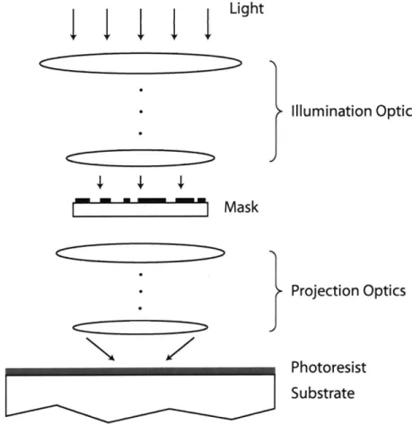
Illumination Optics Mask Projection Optics Photoresist SubstrateFigure 1-1: Schematic of an optical projection lithography system. The mask-based system images the predefined mask pattern onto the substrate of a photoresist-coated substrate, thereby reproducing copies of the pattern in the photoresist. Note that the details of both the illumination and projection optical systems are not depicted for simplicity, as these systems are typically comprised of tens of lenses.
onto a substrate coated with a thin photosensitive film (photoresist). In this manner, the mask pattern is replicated onto the photoresist, similar to the stone slab example mentioned above. An example of such a system is the optical projection stepper, which is depicted in Figure 1-1.
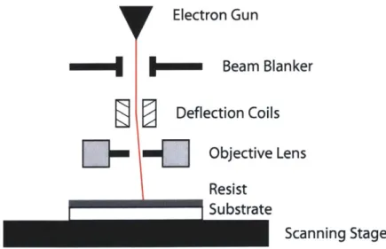
Maskless lithography systems, on the other hand, do not use masks to define patterns onto the photoresist. Instead, lenses are used to focus incident radiation down to a spot on the photoresist, and it is the addition of these discrete spots which eventually forms the desired pattern. Figure 1-2 illustrates this printing technique, where for instance, a line can be defined through the accumulation of collinear discrete spots. An example of such a system is the electron-beam lithography system depicted in Figure 1-3. An electron beam is focused onto the resist coated substrate by means of electric and magnetic fields (the resist in this case is sensitive to electron radiation). A beam blanker is used to turn the electron beam on and off as the substrate is scanned underneath. In this manner, arbitrary patterns can be defined by the addition of discrete spot exposures.
Much of the research to date has been driven by the semiconductor industry, and has centered on the improvement of masked-based lithography systems and its components, from the development of better radiation sources and projection optics, to the enhancement of optical proximity corrections for mask layouts, to the advancement of photoresist chemistries. The reason behind their support for mask-based lithography, such as optical projection lithography, is due to its tremendous throughput advantage
Desired Pattern:
Pixelated Pattern:
Figure 1-2: Depiction of a maskless lithographic printing technique. Patterns, such as the 'MIT' logo, are broken up into discrete pixels. The sequential exposure of these pixels forms the entire pattern. Any arbitrary pattern can be produced in this manner.
-Electron Gun m4 mu Beam Blanker Deflection Coils
E w =J
Objective Lens Resist Substrate-E
Scanning StageFigure 1-3: Schematic of an electron beam lithography system. Note that this is only a partial depiction of such a system, as many components are left out for simplicity. Electrons emitted by the filament gun are focused by a set of objective lenses to a spot on the substrate. The exact location of this spot on the substrate is controlled by deflection coils. Areas out of its deflection range are brought into range using a scanning stage. A beam blanker effectively turns the electron beam on and off allowing for pixels, and thus patterns, to be exposed in an arbitrary manner.
over maskless lithography. Once a particular chip pattern is defined in a mask, it only takes a fraction of a second for a mask-based system to replicate the entire pattern. This same pattern may take a maskless system days, or even weeks, to reproduce. For mass production purposes, throughput is without doubt a critical figure of merit, therefore justifying the actions of the semiconductor industry.
The majority of other lithography users, however, do not have a need for mass production of Integrated Circuits (ICs). In their case, obtaining a mask for each unique design is probably not the most economical or efficient means for performing lithography. Masks on average tend to be very expensive', and it's only getting worse as the technology becomes more advanced and complex [1]. Couple that with the long turnaround time needed for producing masks, and a case for maskless lithography is born. For the majority of lithography users, maskless lithography will save both time and money since each mask will probably be used less than is needed to make up for its cost.
1 On average, each mask set costs in excess of a few thousand dollars. In some instances, mask sets may
cost as much as a million dollars each.
To drive the case home, picture a graduate student feverously working towards a deadline. She does not know for sure if her design will work, so she comes up with multiple iterations to her original design. What should she do, given that all she has access to are mask-based lithography systems? Does she make a mask for each one of her design iterations, thereby wasting valuable money but saving precious time? Or does she make one mask at a time, making another only if the previous design fails, thereby saving money but wasting time? Moreover, even if she has thoroughly thought it through, and has carried out simulations to back up her design decisions, something can and usually will go wrong... I bet she wishes she had to access to a maskless lithography system.
The advantages for eliminating the need for masks do not stop there. The technology required for mask-based lithography systems to compete with maskless lithography systems in terms of performance (resolution, exposure latitude, depth-of-focus) are much more complex compared to that for maskless systems. This complexity makes mask-based lithography systems, on average, cost two to three times more than maskless lithography systems [2].
The increased complexity of mask-based lithography systems also makes modifications to the systems extremely difficult. For instance, changing the radiation source to a shorter wavelength source requires changing the entire illumination and projection optics. While major changes may also need to be made when modifying components to maskless lithography systems, they are generally much less complex.
1.1.1 Maskless Technologies
In the world of maskless lithography, two competing technologies have emerged from the pack - Scanning Spot Technology (SST) and Variable Mask Technology (VMT). SST was used above to explain maskless lithography. In short, radiation is focused down to a
spot on the substrate. By turning the radiation to the substrate on and off while the substrate is scanned on a high precision stage, a set of discrete spots are exposed on the substrate. Any arbitrary pattern can be printed using this technique, since all patterns can be decomposed into collections of discrete spots. VMT, on the other hand, borrows much of its configuration from mask-based lithography systems. Picture an optical
-projection stepper, such as the one depicted in Figure 1-1. Now remove the 'fixed' mask, and replace it with a 'variable' mask. This is the basis of VMT. A 'variable' mask can be programmed to project arbitrary patterns, like a digital projector. In this way, separate masks no longer need to be prepared for each unique design. Instead, arbitrary patterns are defined on a computer, and the computer programs the 'variable' mask to project the desired patterns. Descriptions of systems demonstrating both technologies follow below.
1.1.1.1 Electron-Beam Lithography (SST)
The electron-beam (e-beam) lithography system is the only notable maskless lithography system in production today. It is heavily used in research environments because its ability to pattern without the requirement for masks allows for rapid design prototyping. In addition, these systems provide much higher patterning resolution compared to optical systems 2. Currently, MIT is in possession of two e-beam lithography systems - the
Raith150 and the VS26.
In e-beam lithography, electrons instead of photons are used to chemically alter resist such that areas of the resist exposed to these electrons can be selectively removed with a developing agent. Figure 1-3 previously depicted such a scanning e-beam lithography system. Electrons are irradiated from a filament gun and focused onto the substrate using electric and magnetic fields. Magnetic deflection coils are placed around the path of the electron beam to deflect the beam to different regions of the substrate. Typically, the deflection system can cover an area at most a few hundred microns in size. In order to pattern larger areas, the stage, on which the substrate sits, is scanned. The collection of exposed spots forms a desired pattern.
Although e-beam lithography offers ultra-high-resolution patterning without the need for masks, it suffers from a problem of throughput. For example, the minimum dwell time for a 6nm stepsize on the Raith150 is lOOns [4]. This roughly translates to a writing time of 77 hours for a 1 cm2 area. The same 1 cm2 area can easily be replicated
using just one exposure from an optical projection stepper, taking only fractions of a
second in length. However, for design prototyping, e-beam lithography is still the preferred approach by most lithography users.
1.1.1.2 ASML/Micronic's Maskless Lithography System (VMT)
ASML/Micronic employs the variable mask technique in its Sigma7000 Series maskless lithography tool [5]. Figure 1-4 depicts this system. A spatial light modulator containing
DATA IN PATTERN RASTERIZER LINEARIZED PATTERN BITMAP '4 0SLM ILLU MINATING' LIGHT -PULSED EXIMER LASER BEAM-SPLITTER ' LENS APERTURE LENS INTER-FEROMETER SLM CHIP BEAM SPLITTER LASER PULSE LENS FOURIER FILTER REDUCTION LENS MASK BLANK
Source: Micronic Laser Systems
Figure 1-4: ASML/Micronic's Sigma7000 Series maskless lithography system. The system replaces traditional masks with a spatial-light modulator (SLM), which in effect acts as a variable mask. The SLM consists of a large array of micromirrors, each capable of reflecting light in one of two directions. An aperture is aligned to pass light reflected in one of these directions while blocking light reflected in the other. In this manner, an arbitrary set of pixels, corresponding to the set of micromirrors reflecting light in the appropriate direction, is exposed on the substrate.
a large array of micromechanical mirrors (-4 million) is used to control the illumination
pattern reaching the substrate. Each micromirror in the array is responsible for
controlling the illumination to one pixel on the substrate3. Illumination to these pixels
can individually be turned on and off by electrostatically tilting the micromirrors. An aperture placed between the micromirrors and the substrate serves to only pass light reflected off the untilted micromirrors. In this manner, the computer-controlled spatial light modulator can project any arbitrary pattern onto the substrate.
The rest of the system, i.e. the illumination and projection optics, strongly resembles that of an optical projection stepper. Thus, this system possesses all of the disadvantages listed above for mask-based lithography systems except for those related to the mask. Namely, the system is still extremely complex, and thus inflexible to change.
1.2 Immersion Lithography
Almost everyone has heard of 'Moore's Law,' which states that the number of transistors per square inch on IC chips doubles every year [6]. To keep pace with Moore's Law, lithography tools need to increase their resolution capabilities over this same time period4. According to the International Technology Roadmap for Semiconductors (ITRS), lithography tools are expected to pattern 70nm in 2006, 65nm in 2007, 57nm in
2008, 50nm in 2009, and 45nm in 20105 [7]. Many tool manufacturers have decided to
pursue immersion lithography as a means for meeting these stringent specifications. The benefits of immersion lithography have been known for decades6, but not until recently has there been a real push for bringing this technology to fruition.
In optical lithography, resolution is generally expressed as:
W ki (1-1)
NA
where Wmin represents the minimum attainable linewidth, k, is a proportionality constant which takes into account various system and system variables such as system
non-3 Each micromirror is 1 6pm x 1 6pm in size. Reduction optics is placed between the micromirrors and the
substrate to scale down the size of the illumination projected from each micromirror. 4 Resolution must increase by a factor of V2 every year to keep pace with Moore's Law.
5 Currently, lithography tools are patterning at the 80nm node.
Light
NA
a
sin(max) maSubstrate
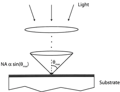
Figure 1-5: A pictorial illustration of the numerical aperture of an optical system.
idealities, resist clipping properties, and environmental conditions, X is the wavelength of the radiation, and NA is the numerical aperture of the optical system. Reducing Wmin can be achieved by decreasing kI, X or by increasing NA. Since k, is a hard to improve, we concentrate on methods for decreasing X and increasing NA.
We first investigate methods for increasing NA. NA is proportional to sin(Omax), where 0
max is the half-angle of the maximum cone of light focused onto the substrate by the last lens of the projection optics (typically referred to as the convergence half-angle).
Figure 1-5 illustrates this definition schematically. We observe from this figure that an
increase in the size of the final lens (in the radial dimension) allows for more light to be focused onto the substrate, resulting in an increase in NA. Unfortunately, there is a limit to this method, as sin(Omax) has a maximum value of 1. Past some point, increases in the
size of the final lens lead to only marginal gains in NA.
Next, we explore possible techniques for reducing X. The obvious approach would be to use a shorter wavelength radiation source. Most lithography systems need to employ a coherent radiation source, i.e. a laser source. Lasers have been around for 45 years, and in that time period, only a small number of different wavelength laser sources have been invented. Thus, we are limited in the wavelength laser sources we can use {= 157nm (F2), 193nm (ArF), 248nm (KrF), 282nm (XeBr), 308nm (XeCl),
-351nm-353nm (XeF), ...}. In addition, problems start to arise in the sub-200nm
wavelength regime. The shortened spatial-coherence length of laser sources in this regime becomes a major concern. A further concern is the degradation in transparency of the projection optics at these lower wavelengths. Optical lenses, typically made of glass or fused silica, become opaque at sub-1 60nm wavelengths.
Another approach for wavelength reduction is immersion of the exposing radiation. The wavelength of the exposing light, X, can be effectively scaled down to k/j by introducing a medium (with refractive index fl) in-between the final lens and the substrate. For the case of air (i = 1), M/r is essentially equal to the wavelength of the radiation source. However, for any other medium (q > 1) between the final lens and the substrate, the exposing wavelength is effectively reduced and the lithographic resolution concurrently improved (by a factor of q) [8]. With the abundance of high refractive index materials available today and many more in development, this immersion scheme presents a very promising approach to improving lithographic resolution.
Reversal of Conventions
It is important to note that in the analysis above, my convention has been to use the refractive index, '9, as a scaling factor for the exposing wavelength. In literature, however, the refractive index is generally coupled into the NA term, i.e. NA = Tnsin(max) [9]. I, nevertheless, find it more logical to introduce the effect of an immersing medium as a reduction of the exposing wavelength, and not as an improvement to NA. However, to be consistent with literature, the remainder of this thesis will take the refractive index into account in the NA equation, and no longer use it as a scaling factor for the exposing wavelength. Hence, the addition of an immersion medium between the final lens and the substrate increases NA (NA can now take on values greater than 1), while X remains equivalent to the wavelength of the radiation source. In the end, both conventions lead to the same results.
1.2.1 An Immersion Optical Projection Lithography System
One of the many benefits of immersion lithography is its ease of implementation into already existent lithography systems. Take the optical projection stepper as an example. Earlier, it was mentioned that mask-based lithography systems, such as the one currently being considered, are so complex that changes to the system are very costly. Integrating an immersion scheme into such systems is one of the few exceptions to the rule.
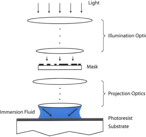
Figure 1-6 depicts an immersion optical projection lithography setup. The schematic is
identical to the non-immersion optical projection setup shown in Figure 1-1, except for the addition of an immersion fluid between the last optical element and the substrate and the modification of a few of the projection optics.
In
just
under a year, IBM has transformed an optical projection stepper, a 0.75NALight Mask
~ccZiiiiz~
}N Immersion Fluid Illumination Optics Projection Optics Photoresist SubstrateFigure 1-6: Schematic of an immersion optical projection lithography system. Notice that the addition of an immersion fluid between the last optical element and the substrate is the only major difference between this system and the system illustrated in Figure 1-1.
-ASML ATI 150i full-field 193nm projection scanner, into an immersion optical projection stepper [10]. They subsequently used this system to demonstrate the successful patterning of one litho-critical via level of their most advanced 90nm, 64-bit PowerPC microprocessor chip set. The completed microprocessors were fully functional and demonstrated better critical dimension uniformity control compared to those fabricated using the traditional non-immersion process. Furthermore, the exposure did not seem to exhibit many of the problems first thought to be potential showstoppers for immersion lithography. One problem, however, was observed - defects due to microscopic bubbles in the immersion fluid. The effects of these microscopic bubbles were only observed in 17% of the chips, so the yield of the immersion process is still comparable to that of the traditional non-immersion process. What IBM has ultimately done, is to demonstrate the relatively short turnaround time needed for successful implementation of an immersion lithography system. This coupled with the immersion scheme's high resolution capabilities make immersion lithography an ideal technology for moving the field of lithography into the next generation.
1.3 The 1V Immersion Maskless Lithography System
To the best of the author's knowledge, the work presented in this thesis describes the first implementation of an immersion maskless lithography system. Maskless lithography and immersion lithography have been investigated for many years, with a number of systems based on these technologies having been developed and many more currently in development. However, so far none of these systems have incorporated both the maskless and immersion concepts into one system. Immersion Zone-Plate-Array Lithography (iZPAL) is the first system to accomplish such a feat. iZPAL employs SST (Scanning Spot Technology) like an e-beam lithography system. However, unlike an e-beam lithography system which uses a single electron beam to expose spots in a serial manner, iZPAL utilizes a massive parallel array of optical beams, giving it a tremendous throughput advantage over most other SST-based lithography systems. The next chapter
Chapter
2
Immersion Zone-Plate-Array Lithography:
System Description and Experimental Operation
Immersion Zone-Plate-Array Lithography (iZPAL) is an innovative optical maskless technology that employs an immersion scheme to further improve its lithographic performance. As was discussed in Chapter 1, most immersion lithography systems are implemented through the modification of existing non-immersion lithography systems. iZPAL is no different in this respect. ZPAL itself is a maskless lithography system, and its configuration is nearly identical to that of iZPAL. Therefore, we proceed by first providing a system description of ZPAL. We then describe the steps used to transform ZPAL into iZPAL. At the very end, a description of iZPAL's experimental setup procedure is provided.
2.1 Zone-Plate-Array Lithography (ZPAL)
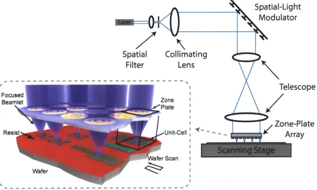
ZPAL is an optical maskless technique that operates on the principle of diffraction rather than refraction. Instead of a single massive lens, an array of thousands of nanofabricated Fresnel zone plate lenses is used, each focusing a beam of light onto the substrate. A
-\Q Spatial-LightModulator Spatial Collimating Filter Lens ,Focused Zn Bearnlet Z'Plne Resist Unit-Cell r Scan Wafer T( Zo elescope ne-Plate Array
Figure 2-1: Schematic of Zone-Plate-Array Lithography (ZPAL). Light emitted from a laser source passes through a spatial filter, which 'cleans up' the beam, before illuminating the spatial-light modulator (SLM). The SLM controls the intensity of light incident on each zone plate of the zone-plate array. The zone plates focus these incident radiation beamlets onto the substrate as the substrate is scanned. Patterns of arbitrary geometries are thus patterned in a 'dot-matrix' fashion.
computer-controlled array of micromechanical spatial light modulators turns the light to each lens on or off as the substrate is scanned under the array, thereby enabling patterns of arbitrary geometries to be printed in a 'dot-matrix' fashion [11-14]. A schematic of ZPAL is shown in Figure 2-1.
The figure above illustrates ZPAL's patterning strategy. Each zone plate is responsible for writing a section of the total pattern'. These sections, labeled 'unit-cells' in the figure above, are written in parallel. The full pattern is then formed through the stitching together of these unit-cells. If we assume that the zone-plate array is as large as (or larger) than the pattern to be written, then the time needed to expose the entire pattern is equivalent to the time it would take for one zone plate to write its unit-cell. Hence,
1 The size of these sections depends on the spacing of the zone plates in the zone-plate array. For densely packed zone plates, the size of these sections is approximately equal to the size of the zone plates.
ZPAL solves the throughput problem faced by most other maskless lithography technologies2.
2.2 ZPAL's Key Components
Figure 2-2 provides a photograph of our prototype ZPAL system along with a block diagram illustrating ZPAL's operation flow. All of ZPAL's key components are labeled in the figure. They are: the radiation source, the spatial light modulator, the zone-plate array, the scanning stage, and the control computer. Each of these components is described in more detail.
2.2.1 The Radiation Source
Zone plates can focus any wavelength radiation with one stipulation - the radiation must be coherent, both temporally and spatially. This requirement narrows our choice of radiation sources down to the limited number of laser sources available today. Of those, the lower wavelength sources are appealing from a resolution standpoint. However, the lowest wavelength sources (sub-200nm) are impractical for ZPAL due to their low spatial coherence lengths and low power outputs. These reasons ultimately led us to choose a 400nm Gallium-Nitride (GaN) solid-state laser. This laser source gives ZPAL the capability of patterning down to sub-200nm features.
2.2.2 The Spatial Light Modulator
The secret behind ZPAL's maskless parallel patterning strategy was revealed at the beginning of this chapter. There, it was mentioned that all the zone plates in the zone-plate array pattern simultaneously, but do so independently of one another. This is accomplished by controlling the intensity of the light incident on each of these zone plates using a micromechanical spatial light modulator placed appropriately between the radiation source and the zone-plate array. Two such technologies have been explored for
2 ZPAL's throughput is still orders of magnitude lower than most mask-based lithography technologies, but
is orders of magnitude higher than many maskless lithography technologies, such as scanning electron beam lithography for example.
-Control Computer
L-4' se
Data Delivery & Grayscale Control s4 Cg SCoq, Radiation Source Spatial-Light Modulator
Silicon Light Machines GLVrM
Zone-Plate Array & Scanning Stage
i-i_
z.
Figure 2-2: Photograph of the prototype ZPAL system. The path of light travel is traced out in 'light blue.' A computer (not pictured) synchronizes the operation of ZPAL's key components, the details of which are outlined in the block diagram.
ZPAL - a Digital Micromirror Device (DMD) manufactured by Texas Instruments and a Grating Light ValveTM (GLVTM) manufactured by Silicon Light Machines [15-16].
The DMD contains over a million independently controlled micromirrors. These micromirrors have the ability to arrange themselves in one of two positions. Normally, the micromirrors are in the 'flat' position. When electrostatic forces are applied to particular micromirrors, those micromirrors rotate to a 'tilt' position. Thus, light incident on this device is reflected in one of two possible directions. This technology can be utilized in ZPAL to control the light incident to each zone plate. A schematic of the DMD's implementation in ZPAL is shown in Figure 2-3. The micromirror array is aligned such that light reflected off the micromirrors in the 'flat' position are incident normal to the zone-plate array while light reflected off the micromirrors in the 'tilt'
Mirror Incident Radiation
0
Zone-Plate Array
Su bstrate Stage
Figure 2-3: Implementation of the Digital Micromirror Device (DMD) in ZPAL. Each micromirror can arrange itself in one of two positions, and can therefore reflect light in one of two directions. The DMD is aligned such that light traveling in one of the two reflected directions is normally incident on the zone-plate array, while light traveling in the other reflected direction misses the zone-plate array.
-Silicon Light Machines GLVTM GLV
Fixed Ribbon
Zone-Plate
Movable Ribbon Array
Electrode Substrate
Stage
(a) (b)
Figure 2-4: Implementation of the Grating Light ValveTM (GLVTM) in ZPAL. Each
GLVTM pixel depicted in (a) can either form a planar surface to reflect light or a grating
to diffract light. The GLVTM is aligned such that light diffracted into the +1 order is normally incident on the zone-plate array, as illustrated in (b). Thus, the GLVTM effectively turns light to the zone plates on. and off by diffracting or reflecting light respectively. Note that the amount of light diffracted into the +1 order can also be controlled by appropriately adjusting the depth of its grating.
position propagate away from the zone-plate array3. Telescoping optics are placed between the micromirrors and the zone-plate array to map one micromirror to one zone plate.
In contrast to the DMD, the GLV is a diffraction-based technology comprised of over a thousand independently controlled elements. Each GLV pixel consists of six Aluminum (Al) ribbons in parallel. When inactivated, the GLV pixel acts like a mirror and reflects light at an angle equal to the angle at which it was incident. When activated, however, electrostatic forces are used to pull down alternating ribbons of the GLV pixel, forming a phase grating. Light incident on this grating will diffract in many different angles, i.e. diffraction orders. Since light diffracted in these diffraction orders can be turned on and off by simply activating or inactivating the GLV pixel, such a technology
3 The DMD can be also be aligned so that micromirrors in the 'tilt' position reflect light to the zone-plate
can be used in ZPAL to control the light incident to each zone plate. A schematic of the GLV's implementation in ZPAL is shown in Figure 2-4, along with a depiction of one GLV pixel in operation. The GLV is aligned such that the +1 diffraction order is incident normally on the zone-plate array. All other diffraction orders, including light reflected off a non-actuated GLV pixel, are deflected away from the zone-plate array. As was done with the DMD, telescoping optics are placed between the GLV and the zone-plate array to map one GLV pixel to one zone plate.
The GLV technology has some inherent advantages over the DMD technology for ZPAL. The process used by the GLV for switching light to a zone plate (ribbon pull-down) is intrinsically much faster than that used by the DMD (micromirror tilting). For a quantitative comparison, it takes the DMD 20ps to turn off light to a zone plate, while it only takes the GLV 20ns. That's a three orders of magnitude improvement! The GLV also has built-in grayscaling4, something the DMD does not. Grayscaling in the GLV is accomplished by controlling the depth at which the ribbons are pulled down. This, in effect, determines the amount of light diffracted into the +1 order. These two advantages make the GLV a better multiplexing element for ZPAL, and is currently being used as such [17].
2.2.3 The Zone-Plate Array
The zone plates are the single most innovative and important part of the ZPAL system, as they are largely responsible for the system's lithographic performance. ZPAL departs from century old refractive technologies in introducing the use of diffractive optics, i.e. zone plates, for lithography. We discuss the differences between these two technologies below. The zone plate, however, deserves its very own chapter, so we hold off on its analysis until the next chapter.
4 Grayscaling is used to correct for any variations in the efficiencies of the zone plates. It is also important for applications such as proximity effect correction (PEC).
-2.2.3.1 Diffractive vs. Refractive Lens Technologies
Zone plates can simply be thought of as optical lenses. They behave very much like traditional optical lenses, but differ in one important respect - they use the principle of diffraction, not refraction, to focus light. Light, being a wave, has two components - an amplitude and a phase component. The phase component is the key to diffraction theory. As a motivating example, imagine two waves with equal amplitudes traveling in parallel. These waves, although equal in amplitude, will cancel each other out if their phases differ by a radians. Now it's clear how diffractive lenses work to focus light - they constructively interfere all transmitted light at its focal point. Light that would normally destructively interfere at this point is either blocked or manipulated to constructively interfere there. It is for this reason that diffractive lenses need coherent illumination.
Refractive lenses, on the other hand, operate under Snell's Law, i.e. incident light is bent in varying degrees so that it all crosses at a common point. Figure 2-5 illustrates this process. The curvature of refractive lenses is designed such that light further from the optical axis is bent more than light closer to the optical axis, leading to a common crossing point. Snell's Law:
m,
sin(01) = 92 sin(02) 01 112 Focal Point Refractive LensFigure 2-5: The refractive process for focusing light. A refractive lens bends light according to Snell's Law. Its curvature, which determines the degree of light bending, can therefore be designed to direct all incident light to a common point.
Diffractive lenses have numerous advantages over refractive lenses, due in large part to the superior fabrication techniques used for their production. Diffractive lenses are made using nanofabrication processes, where dimensions can be controlled to the nanometer scale. Refractive lenses, on the other hand, continue to rely on ancient techniques such as mechanical polishing. These techniques are not as precise as the ones used to produce their diffractive counterparts. Nanofabrication processes are also much more repeatable. As a result, better uniformity can be achieved across a larger array of diffractive lenses. As a further advantage, nanofabrication processes exhibit nanometer placement accuracy, which is extremely important for stitching together fields exposed in parallel (ala ZPAL). One final advantage diffractive lenses have over refractive lenses is its scalability to lower and lower wavelengths. Refractive lenses, because they are typically made of glass or fused silica, become opaque at sub-i 60nm wavelengths.
2.2.4 The Scanning Stage
A precision scanning stage is used to raster scan the substrate during an exposure. The stage positioning accuracy plays a major role in determining how close exposed patterns are to ideal. It affects critical dimension control, pattern placement, and stitching. The scanning stage must also have enough range to scan an area the size of a unit-cell. With this in mind, we chose the Piezo Flexure Nanopositioning Scanner from Physik Instrumente (model P-770), which offers a scan range of 200pm x 200tm and a positioning accuracy of less than 10nm. Velocity feedback circuits were then custom built to enable continuous-velocity scanning of the stage. The continuous scan mode vastly improves exposure times (throughput).
2.2.5 The Control Computer
A computer equipped with LabVIEW software and controllers for the spatial light modulator and scanning stage is used to run ZPAL. A custom-written LabVIEW program handles the exposure. First, the pattern to be exposed is encoded in a readable format and loaded into the LabVIEW program. The program then divides the pattern into unit-cells and sends the appropriate data to each pixel of the spatial light modulator. It
-___________________________ -~-4-~- -~
simultaneously synchronizes the motion of the scanning stage so that everything works in unison.
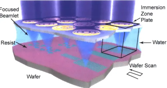
2.3 Transforming ZPAL into iZPAL
iZPAL is depicted in Figure 2-6. The system depicted in this figure is very similar to the non-immersion ZPAL system depicted in Figure 2-1. There are, however, two major differences between the systems. The more obvious of the two differences is the change in the medium between the zone-plate array and the substrate from air (ZPAL) to a high-index immersion fluid such as deionized-water (iZPAL). The other difference, which may not be immediately apparent from looking at the two figures, is the zone plates themselves. The medium in which the zone plate focuses its radiation influences its design. Thus, the zone plates used in ZPAL cannot be used in our immersion experiments.
Replacing the air between the zone-plate array and the substrate with
deionized-Focused
Immersion
Beamlet
Zone
'Plate Resist WaterWafer Scan
WaferFigure 2-6: Schematic of Immersion Zone-Plate-Array Lithography (iZPAL). The space between the zone-plate array and the substrate is filled with DI-water. An array of specially designed zone plates focuses incident radiation beamlets through the water and onto the surface of the substrate. The rest of this system's operation is identical to that of the non-immersion ZPAL system.
water (DI-water) is not as simple as it may appear. The zone plates are designed to have a focal length of 40pm. Thus, the gap between the zone-plate array and the substrate is too small to push DI-water in through its sides. Instead, a micropipette is used to place a drop of DI-water (volume ~ 800nL) onto the substrate. The zone-plate array is then aligned to the droplet using a bright-field microscope and lowered until a gap of 40gm is reached. The small gap prevents rapid evaporation of the DI-water into the surrounding air, allowing exposures that are hours in length to be completed with only one droplet of DI-water.
The redesign of the zone plates for this new medium is fairly straightforward. It requires nothing more than changing the value of one parameter in the design. The fabrication of these new zone plates, however, is another story. The process used for the fabrication of non-immersion zone plates cannot be used for the fabrication of immersion zone plates for reasons explained later. Therefore, a new fabrication process with new starting materials was developed. The zone plate design and fabrication process is discussed in further detail in the next chapter.
2.4 Experimental Setup Procedure
A step-by-step procedure for setting up an iZPAL exposure:
" Place a silicon wafer coated with Barli anti-reflection coating (200nm) and PFI-88 photoresist (1 00nm) on the scanning stage.
" Turn on the vacuum to the scanning stage to prevent the substrate from moving. " Parallelize the zone-plate array to the substrate.
* Add a droplet of DI-water onto the substrate using a micropipette.
" Align the zone-plate array to the water droplet using a bright-field microscope. " Lower the zone-plate array onto the water droplet using a z-stage.
" Gap the zone-plate array to the substrate.
" Run the exposure using the custom LabVIEW program.
The parallelization and gapping of the zone-plate array to the substrate are explained in more detail below.
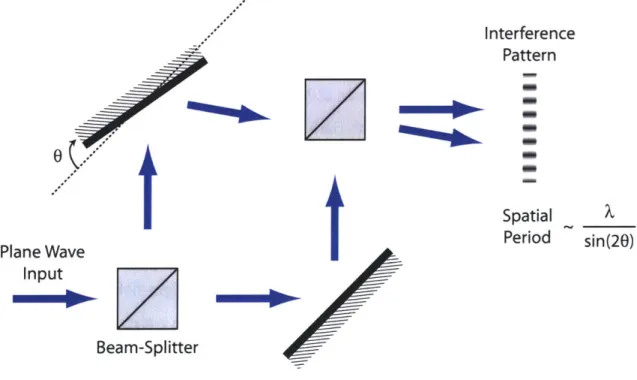
-2.4.1 Parallelization
The zone-plate array needs to be parallel with the substrate to ensure that all the zone plates in the array can be properly gapped. The depth-of-focus of our zone plates, i.e. the maximum distance away from a zone plate's focal plane such that its focused light is only marginally degraded, is no more than a few hundred nanometers. The zone-plate array, however, can be millimeters or even centimeters in both length and width. Therefore, even the slightest of tilts5 will cause non-uniform patterning across the zone plates in the
array (that is, if they pattern at all). For example, assume the zone-plate array is 1mm x 1mm in size. A mere tilt of 0.1 degrees corresponds to a 1.75prm difference in gap between zone plates located on opposite ends of the zone-plate array.
A technique that can detect even the slightest of tilts is needed. The Mach-Zender interferometer does this. Figure 2-7 illustrates a typical Mach-Zender setup, which is nearly identical to the one used for iZPAL. In this interferometer, light reflected off two
Plane Wave Input Beam-Splitter Interference Pattern
z
Spatial _ Period sin(20) 'AFigure 2-7: A Mach-Zender interferometer setup similar to the one used to parallelize the zone-plate array to the substrate.
5 'Tilt' in this context means the relative tilt of the zone-plate array in reference to the substrate.
.... ...
"ftftwobil-unparallel surfaces will interfere and display interference fringes at the detector. The period of these fringes, given that one surface is tilted 0 degrees in reference to the other, is X/sin(20). Therefore, we can minimize the tilt, 0, by maximizing the period of the fringes seen at the detector. In my experiments, a maximum fringe period was a few millimeters, which corresponds to a tilt of 0.005 degrees (parameters used: fringe period = 4mm, X = 632.8nm).
2.4.2 Gapping
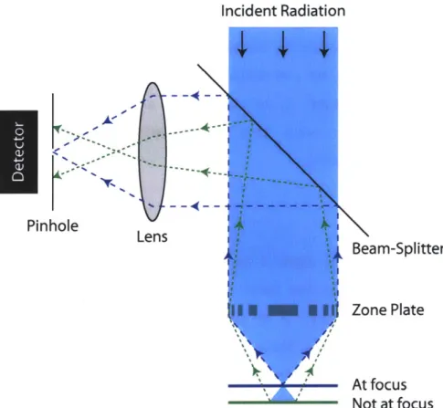
As mentioned above, the depth-of-focus of our zone plates is at most a few hundred nanometers. This implies that there's little room for error in the gapping of the zone-plate array to the substrate. If the gap is off in either direction by more than a few hundred nanometers, the zone plates won't pattern properly or won't pattern at all.
It turns out that zone plates can be used for confocal microscopy [18]. Figure 2-8 illustrates such a setup. We exploit this property of zone plates to accurately gap them to the substrate. Light incident on the zone plates is focused onto the substrate. Some of this light reflects back from the substrate and is reimaged by the zone plates. At precisely the correct gap, the zone plates focus incident light down to a spot on the substrate and recollimate all the light reflected back. A second lens (refractive) and an aperture are positioned such that the light recollimated by the zone plates is focused by this second lens down to a spot at the aperture. The aperture blocks light reimaged by the zone plates at all other gaps. Therefore, a detector placed on the other side of the aperture will detect a signal only when the zone plates are perfectly gapped to the substrate.
There is one additional complication. The gapping procedure described above relies on the projection and reflection of light onto and back from the substrate, exposing the photoresist in the process. Therefore, this procedure can only be performed using a
6
wavelength light to which the photoresist is insensitive . Zone plates designed to focus this new radiation (HeNe) are fabricated together with the zone-plate array and appropriately positioned around its perimeter. Proper gapping of the HeNe zone plates
6 The photoresist used in our experiments, PFI-88, is insensitive to HeNe light (X=632.8nm).
-Incident Radiation A" Pinhole ---4--. ---4--. Beam-Splitter Zone Plate At focus Not at focus
Figure 2-8: The confocal microscopy setup used to gap the zone-plate array to the substrate. The zone plates themselves are used to image light reflected back from the substrate. In the setup, only light re-collimated by the zone plates pass through the pinhole and reach the photodetector. The zone plates only re-collimate the back-reflected
light when they are perfectly gapped to the substrate.
ensures the proper gapping of the zone-plate array since both sets are designed to have the same focal length.
Lens
Chapter 3
Zone Plates:
Theory, Design, and Fabrication
Although the application of zone plates for lithography has only very recently been proposed and investigated, zone plates themselves have been around for over a century. Zone plates were derived from the work of Fresnel, particularly his concept of Fresnel zones, in the 1800's. To this day, it is unknown who first succeeded in experimentally demonstrating its proper functionality, though there are a few theories as to who it may be. For instance, Lord Rayleigh of 'Rayleigh Scattering' fame wrote in a notebook entry on April 1 1th, 1871: "The experiment of blocking out the odd Huygens zones so as to
increase the light at centre succeeded very well" [19]. Today, however, most people give Fresnel the credit to the discovery of these diffractive optical elements and refer to them as Fresnel zone plates. The rest, as the say, is history.
-3.1 Zone Plate Theory
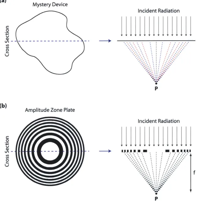
As has been mentioned numerous times in the past, zone plates focus light using the principle of diffraction. Light, being a wave, has two components - an amplitude and a phase component. It is the phase component which is key to diffraction. I've used the following example before to motivate this point: Imagine two waves with equal amplitudes traveling in parallel. These waves, although equal in amplitude, will cancel each other out if their phases differ by 71 radians. Therefore, one can think of a zone plate as a device which manipulates light in a manner such that all light constructively interferes at its focal point.
Let me clarify the previous statement schematically (see Figure 3-1). First, imagine light incident normally (plane wave) on a device which is either circular, rectangular, or any other arbitrary shape. Light passes through this device and continues on its way, but not before it is altered in some manner. The device, it turns out, has manipulated the light such that all the light constructively interferes at P (the focal point of the device). The question now is, how does the device achieve this?
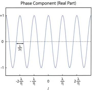
For the explanation, we once again examine the phase component of light, since it is this component which determines the light's constructive or destructive behavior. The phase component is expressed as:
e ,) (3-1)
where 1 represents the distance traveled by the light [20]. Figure 3-2 plots the real part of this phase component as a function of 1. Two important observations are made from this plot. First, the phase component is periodic with period equal to X/1. Second, the phase
component takes on positive values for a span of %,/2fl, then negative values for a span of X/2rj, then positive values again for a span of k/21j, and so on and so forth. These two properties of the phase component help explain the zone plate's operation.
(a)
C 0 0I
IF
III
Incident Radiation1111111111
r,
,FI
IV
I
Mystery DeviceAmplitude Zone Plate
Incident Radiation
>- I m ,m,E 'EIEm ,
I /1
IF
Figure 3-1: The amplitude zone plate. (a) An arbitrarily shaped 'mystery' device focuses incident radiation down to a spot at P. (b) An amplitude zone plate behaves just like this 'mystery' device in focusing incident radiation down to a spot at P. The dark areas of the zone plate serve to block out light which would otherwise destructively interfere at P, allowing for the constructive interference of all light at P.
Now let's journey back to the discussion concerning the yet-to-be-determined device illustrated in Figure 3-1(a). The figure also depicts several dotted lines connecting different points on the device to P, representing paths traveled by the light in
-41-otI ~il P
(b)
0 0 UI
fPhase Component (Real Part) +1
-1--2 - 0 2
TII Ti
Figure 3-2: A plot of the real part of the phase component expressed in Eq. 3-1.
getting from the device to P. Light originating at precisely the midpoint of the device (black) exhibits some phase at P, be it positive or negative. For the sake of argument, let's say it's positive'. Then, light originating in close proximity to the midpoint of the device (blue) will also exhibit positive phases at P, since the differences in distance between their optical paths and the 'black' optical path are less than X/29. Light originating from these areas, therefore, constructively interfere with each other and with the light originating from the midpoint of the device, at P. However, as we move further away from the center of the device, a point will arrive where the light originating from that point (red) starts to exhibit negative phases at P and destructively interferes with the positive-phase light present at P. If we continue to move even further away from the center of the device, another point will arrive where the light originating from that point (blue) once again starts to exhibit positive phases at P. These sign changes are due to the periodicity of the phase component of light as discussed above, and will continue until the end of the device is reached.
We are now ready to unravel the mystery of a zone plate. A zone plate, which the mysterious device in Figure 3-1 (a) portrays, does one of two things to ensure that no
1 This is completely arbitrary and does not limit the outcome of the resulting analysis to this specific case.