Design and Implementation of the Alewife Startup Module
byWilliam K. Chan
S.B., Electrical Science and Engineering
Massachusetts Institute of Technology
Submitted to the
Department of Electrical Engineering and Computer Science in Partial Fulfillment of the Requirements of the Degree of
Master of Engineering in Electrical Engineering and Computer Science at the
Massachusetts Institute of Technology June 1995
© 1995 William K. Chan. All rights reserved.
The author hereby grants to MIT permission to reproduce and to distribute publicly paper and electronic copies of this thesis
document in whole or in part.
Author
Department
Certified by
Accepted by
of Electrical Engineering and Computer Science iMay25, 1995
·' !4 '~ Anant Agarwal
Thesis Supervisor
| ''~r<e ic R. Morgenthaler
C j'Sk~t Commi tee n Graduate Theses
Design and Implementation of the Alewife Startup Module
byWilliam K. Chan
Submitted to the
Department of Electrical Engineering and Computer Science
May 25, 1995
In Partial Fulfillment of the Requirements for the Degree of Master of Engineering in Electrical Engineering and Computer Science
ABSTRACT
The Alewife prototype uses a host connected via a VME bus for its communi-cations. This configuration is a bottleneck for operations which require exter-nal devices. A method to use SCSI has been developed, but it cannot fully replace the startup sequence generated by the VME-based host. The focus of
this thesis is to design and implement the necessary hardware and software to
perform the startup sequence, allowing the removal of the VME interface. In
addition, the clock synthesizer from the VME transceiver board will be enhanced and incorporated into the startup module to consolidate hardware. Thesis Supervisor: Anant Agarwal
Title: Jamieson Career Development Associate Professor of Computer Science
Acknowledgments
Thanks go to Professor Anant Agarwal for his guidance and support throughout this thesis. Also, Ken Mackenzie was extremely valuable by
help-ing with all aspects of design and testhelp-ing, from explainhelp-ing the design tools to writing some test code of his own. He was a wonderful source of advice and
information.
In addition, a special thanks go to my parents, Raymond and Lily Chan, for their continuing emotional and financial support.
Table of Contents
Chapter 1...Chapter 2...
Chapter 3...
Chapter 4...
Chapter 5. Chapter 6. Chapter 7. Appendix A Appendix E Appendix C References Introduction Background Overview... System Requ: Startup Engi Clock Synthe System Issue Hardware De Startup Engi: Clock Synthe Additional HI Board Design Software Des Global Setup Startup Engi Clock Synthe.... Testing
....
Startup Engi Clock Synthe .... Startup Modi.... Conclusion
.
Summary .. Future Work L ... ABEL Code f 3 ... Phase-Lockec J... Startup Modi
I . . ·. .. . . e ·. ·. · . . . 5 . . . 5 . . . 7irements
...
9
ne ... 9 sizer ... 10 s ... 12.sign and Implementation ... 13
ne ... 13
sizer ... 16
ardware
...
19
and Layout ... 22
ign and Implementation ... 23
...
23
ne ... 25sizer
...
26
...
30
ne ... 30sizer
...
31
ule Operation ... 33...
34
...
34
...
34
or 22V10 PAL ... 36d Loop Design Calculations ... 37
ule Software ... 38
...
47
...
...
Chapter 1
Introduction
Background
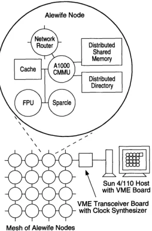
The Alewife machine is a large-scale distributed-memory multiproces-sor organized as a set of processing nodes connected in a mesh topology. Each node consists of a processor, a cache, a portion of globally-shared distributed memory, a cache-memory-network controller, a floating-point coprocessor,
and a network switch. Free network ports on peripheral nodes of the mesh
are used for I/O, monitor, and host connections. The Alewife prototype
attaches to a host Sun 4/110 by interfacing a network switch to the VME bus.
A block diagram of the Alewife prototype is shown in Figure 1-1 [1].
This configuration is a bottleneck for operations which require external devices since all external access is handled through the host computer. Thus,
the next step in the development of Alewife is to improve its communications capabilities. One method involves the addition of new non-processing nodes capable of SCSI communication. This not only enhances the communications
capabilities of the machine by increasing connections, but also provides a more common interface standard by using SCSI rather than VME.
The addition of the SCSI nodes provides an opportunity to enhance the
Alewife environment. With the presence of the SCSI interface, there is very little use for the old VME interface. In fact, the only task that does not have a SCSI equivalent is the startup sequence since it depends on the direct link
Mesh of Alewife Nodes
Figure 1-1: Block Diagram of Alewife Prototype
between the mesh network switch and VME bus. SCSI nodes can be consid-ered to be specialized processing nodes and need to receive startup
informa-tion themselves so they cannot initiate the startup sequence. However, it is unreasonable to maintain a VME-based host for the sole purpose of starting up the machine.
The focus of this thesis is the design and implementation of hardware and software to support the SCSI-capable Alewife machine such that it can function without a VME interface. This includes performing the startup
sequence and generating the system clock which are functions of the VME
Overview
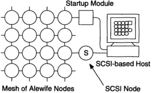
The startup module is a stand-alone hardware and software unit which
enhances the Alewife machine by allowing it to startup without external resources. In particular, it eliminates the need for a VME-based host
com-puter to execute the startup sequence. Instead, it contains a startup engine in hardware and interfaces directly to a peripheral node of the Alewife machine through an unused network switch port. In addition, an improved version of
the clock synthesizer located on the VME transceiver board is included to con-solidate hardware. A block diagram of the new Alewife system is shown in Figure 1-2.
Startup Module
lost
Mesh of Alewife Nodes SCSI Node
Figure 1-2: Block Diagram of New Alewife System
The startup engine is designed to be invisible to the user in its
opera-tion. It automatically sends startup information to the node whenever the Alewife machine is reset. Its major components are a microcontroller unit (MCU) and an electrically-erasable programmable read-only memory (EEPROM). The EEPROM contains both the software for the MCU and the
easily, making it simple to add software features to the startup module and update the Alewife startup information.
The clock synthesizer in its default mode of operation is also
transpar-ent to the user. It is responsible for providing the system clock for the Alewife
machine as a differential positive ECL (pECL) signal. The system actually consists of a MCU-controlled phase-locked loop (PLL) which generates a stan-dard ECL signal at a default frequency of 40 MHz. The clock frequency can be adjusted within a range of 5 MHz to 80 MHz by the user. Control is
Chapter 2
System Requirements
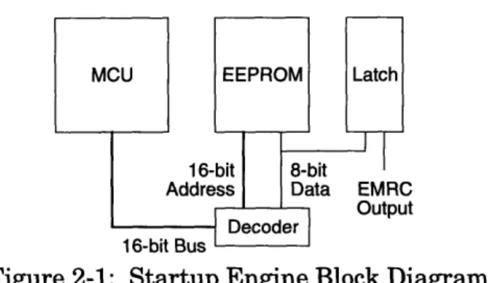
Startup Engine
The purpose of the startup engine is to send startup information
directly to an Alewife processing node. It consists mainly of a Motorola 68HCll MCU and an EEPROM. A block diagram of the startup engine is
shown in Figure 2-1. The 68HCll operates in its expanded multiplexed mode in order to access the EEPROM. The EEPROM contains both the software for the 68HCll and the Alewife startup information. In expanded multiplexed mode, the 68HCll is capable of fetching its instructions directly from the
EEPROM, making software updates to the 68HCll very easy.
Figure 2-1: Startup Engine Block Diagram
The operation of the startup engine requires a direct connection to an
unused network switch port. The network switch used for Alewife processing nodes is the Elko Mesh Routing Chip (EMRC) from the California Institute of Technology [2]. The EMRC uses eight-bit channels and operates
star-tup engine needs to be able to reset the Alewife machine, requiring one
additional signal. The hardware interface from the 68HCll cannot be accom-plished by only using its built-in ports. Expanded multiplexed mode occupies 16 I/O pins, leaving only eight digital pins available and the interface requires at least ten outputs. In order to solve this, a latch connected to the data bus
can be used to provide additional outputs. The latch can load values from the data bus to use as outputs. However, this method of generating outputs is not glitch free, but it is sufficient for the 8-bit EMRC data channel which is not
continuously sampled.
The specifics of the network switch protocol are handled by the 68HC 11
software. The primary concern in communicating with the EMRC is the handshaking protocol since the EMRC operates asynchronously. In particu-lar, the protocol expects a data transfer at each transition of the handshake.
Clock Synthesizer
The clock synthesizer is responsible for providing the clock signal for the entire Alewife machine. The signal generated conforms to pECL voltage levels and is configurable from 5 MHz to 80 MHz. The synthesizer is built around a programmable PLL which interfaces directly with a 68HC11. The
68HCll provides the user interface to adjust the frequency of the clock signal.
The PLL generates a signal at standard ECL voltage levels and requires con-version to the pECL levels expected by the Alewife machine. A block diagram
Figure 2-2: Clock Synthesizer Block Diagram
The clock synthesizer is based on the one located on the VME
trans-ceiver board [3]. Its design centers around the Motorola 145170 PLL Fre-quency Synthesizer with Serial Interface. The 145170, along with a VCO and
a low pass filter, form the PLL which is interfaced serially to the 68HC11.
The 68HCll adjusts the frequency of the PLL by changing the value of a con-trol register in the 145170.
The PLL is not capable of generating the entire frequency range desired due to the limits of the VCO. In order to ensure a valid signal throughout the
desired range, the PLL is only designed to generate signals from 20 MHz to 80 MHz. The frequencies from 5 MHz to 20 MHz are then generated by dividing
the PLL output by four using an ECL divider. The desired signal is then
selected with a multiplexer. The accompanying software makes the entire
fre-quency range appear continuous to both the Alewife machine and the user. The clock synthesizer also has voltage requirements unique to the Ale-wife environment. The CMOS and TTL parts use +5 V and ground, but the ECL parts require -5 V. Although the power supply for the startup module
does not generate -5 V, it does provide -12 V. A voltage regulator is used to
generate the appropriate voltage level for the ECL parts.
System Issues
Both the design of the startup engine and the clock synthesizer utilize the 68HC11. Therefore, it is logical to try using the same part for both sys-tems. From the software perspective, this is not a problem since each one uses minimal 68HCll resources. However, there is hardware limitation in the number of output pins available. This can be alleviated by adding another latch to capture values from the data bus, similar to the latch used for the EMRC data in the startup engine. This provides eight additional outputs for
general use. These outputs can only be used for signals which can tolerate
glitches. Otherwise, a direct interface to the 68HCll is required.
In addition to the startup engine and the clock synthesizer, several sup-porting applications can be developed for the startup module. In particular, a
power supply controller requires only six I/O signals and which can be
con-trolled through software by the 68HC11. Also, the Port E of the 68HCll is
Chapter 3
Hardware Design and Implementation
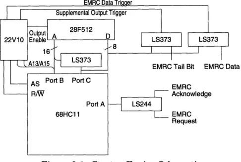
Startup Engine
The startup engine is comprised mainly of the 68HC11, an EEPROM,
and various parts for use in inputs and outputs. Specific parts used are the
28F512 EEPROM, 22V10 programmable array logic (PAL), LS244 buffer, and LS373 latch. All of the general logic necessary in the startup engine can be
implemented within the PAL, saving many general logic parts. The schematic
for the startup engine is shown in Figure 3-1.
)ata
Figure 3-1: Startup Engine Schematic
In the normal operation of the startup engine, the 68HCl11 is in its
expanded multiplexed mode [4]. This allows it to access the EEPROM by
bits and the 8-bit data is multiplexed with the lower eight bits of the address. The address, R/W, and AS are active and valid for all bus cycles including
accesses of internal addresses.
The address decoding in expanded multiplexed mode is essentially
han-dled by one signal. The AS signal from the 68HC11 is used as the trigger of a
LS373 latch. This LS373 latches the lower address bits when AS is high, ensuring its availability during the data portion of the cycle. The R/W signal is used to determine the direction of data transfer on the bus.
A timing diagram for a typical 68HCll bus transaction is shown in Fig-ure 3-2 [5]. The E clock generated by the 68HCll establishes the rate for bus
cycles. In the startup module, the E clock frequency is 2 MHz. The address bits are available each E clock cycle while the clock is low. The AS occurs
dur-ing this half cycle, allowdur-ing the LS373 to latch the lower address bits. In the
next half cycle while the E clock is high, the data is active and can be
consid-ered valid at the falling edge of the E clock.
E
R/W, Address< > Address/Data Read Address
Address/Data Write 8 Address AS
Figure 3-2: Data Bus Timing Diagram
The LS244 is used for buffering inputs and outputs between the 68HC11 and external elements. By buffering outputs, the LS244 becomes the part driving and receiving signals, insulating the 68HC11 from abnormal
volt-age levels. This is especially useful for signals which interact with other
com-ponents of the Alewife machine not resident on the startup module.
The two LS373 latches which are used as additional outputs are
con-nected directly to the data bus. The latches capture values from the data bus which are used as outputs to devices which are not glitch sensitive. The trig-gers to these latches are generated from the PAL. These trigtrig-gers are based on the address targeted when the data is placed on the bus, as well as the R/W signal and the E clock. Depending on the particular address, either latch may be activated to capture the values from the data bus. The implementation only requires two address bits to decode which latch, if either, should be
trig-gered.
The PAL is used for general combinational logic. Signals with a direct
influence on the startup engine are the Alewife reset signal, the latch triggers, and the EEPROM output enable signal. The Alewife reset signal is generated by the 68HCll and initialized low when the startup module is turned on. However, the signal should be initialized high so the PAL inverts the 68HCll signal before it is driven to the EMRC. The latch triggers and the EEPROM output enable signal are all designed to be active during the data portion of the E clock cycle. The EEPROM output enable is activated whenever it is a read operation, and the latch triggers are active on write operations to
partic-ular address locations. The exact implementation of each of these signals is included in Appendix A.
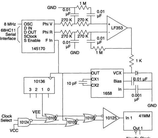
Clock Synthesizer
The clock synthesizer generates the signal used as the Alewife system
clock. Frequencies from 5 MHz to 80 MHz are supported by the synthesizer. Voltage levels produced are designed to meet pECL standards. Frequency changes by the synthesizer are smooth enough so that it can be changed while
the machine is running without causing harm.
The clock synthesizer is built around a configurable PLL which gener-ates an ECL signal between 20 MHz and 80 MHz. The output of the PLL is divided by four in order to generate frequencies between 5 MHz and 20 MHz. The combination of these two outputs provides the full frequency range speci-fied. The desired signal is selected using an 2-to-1 multiplexer. The output is then converted to pECL voltage levels in two stages. A schematic of the clock
synthesizer is shown in Figure 3-3.
The main component of the PLL is the 145170 [6]. This application-specific part contains most of the circuitry necessary for a configurable PLL,
including a built-in serial interface compatible with the 68HC11. The PLL is completed with the addition of a VCO and a low pass filter. In this case, the VCO is the Motorola 1658 and the low pass filter is an active integrator built
around a LF353 operational amplifier. The design of the PLL follows an example in the Motorola data book closely [7]. One of the important
parame-ters is the resulting jitter in the PLL. This will provide a better signal, although it may result in a very long time-to-lock. However, the time-to-lock
1 M GND 0.01 mmC0A 0.01 81\ 68H( SE Interf; Cloc Selec JD Alewife Clock
Figure 3-3: Clock Synthesizer Schematic
to minimize jitter. The details of the calculation of the PLL parameters are included in Appendix B.
Dividing the output of the PLL to generate the 5 MHz to 20 MHz range is straight forward with a good selection of ECL parts available. A simple
method is to use the 10136 universal hexadecimal counter. By using the PLL output as the clock input to the 10136, the second least significant bit is
equiv-alent to the clock divided by four when the counter is configured to count
con-tinuously [8].
The next step is to select the appropriate clock with a 2-to-1 multi-plexer. Since the select signal will be at TTL voltage levels, the easiest
method is to build a special multiplexer from standard logic parts. As a result, a 10105 triple 2-3-2 input OR/NOR gate and a 10124 TTL to ECL
translator were used. The 10124 is capable of providing both the translated
value and its complement, making the design of the multiplexer a little
sim-pler. The two 2-input OR/NOR gates are used to select the signal to be passed
through, and the remaining 3-input OR/NOR is used to combine the two sig-nals. Both the output signal and its complement are used for the conversion
to pECL voltage levels.
The converter to pECL voltage levels is built in two stages. The first
stages uses the 10125 ECL to TTL translator. The 10125 requires both the input signal and its complement to function optimally. Fortunately, the
10105 is capable of providing the necessary signals. The output of the 10125 is then input into the AT&T 41MM transceiver. The 41MM converts from
TTL to pECL voltage levels and outputs both the signal and its complement
[9]. The result is a differential clock for the Alewife machine at pECL voltage levels.
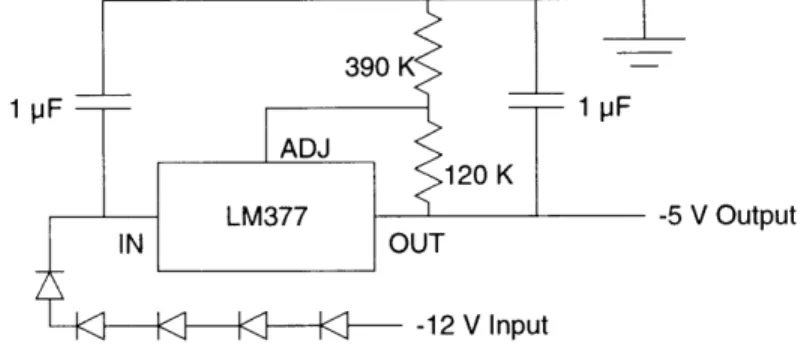
By using ECL parts in the implementation of the clock synthesizer, it is
also necessary to provide the appropriate voltage levels. The power supply for the startup module happens to provides -12 V for its negative voltage source. It is necessary to build a voltage regulator to provide the -5 V supply needed for ECL logic. In this case, the LM337 adjustable regulator is used to perform the conversion. The design is based on an example obtained from the LM337
Fig-ure 3-4. The first step in the conversion is a series of five diodes, providing an initial voltage change to approximately -8 V from the original -12 V. The LM337 is then used to regulate the voltage more precisely. The voltage change provided by the diodes reduces the voltage change required for the
LM337, distributing the power dissipation among the parts.
V Output
Figure 3-4: Voltage Regulator Schematic
Additional Hardware
There are several pieces of supporting hardware which are also critical
to the overall operation of the startup module. These include the EMRC
con-nector, RS-232 serial interface, the reset circuitry, and the hardware mode selector. In addition, hardware support for a power supply controller and the use of the analog port of the 68HCll have been implemented on the startup
module.
EMRC Connector
The connector which interfaces with the Alewife node is a 60-pin ribbon cable connector. It contains connections for the EMRC communications
proto-col, the Alewife reset signal, and the differential clock signal generated by the
clock synthesizer.
RS-232 Serial Interface
The RS-232 serial interface is a fairly simple design. In this particular
case, the Maxim 233A is interfaced directly with the 68HCll [11]. The 233A is capable of converting between TTL and RS-232 voltage levels and is an ideal one-part solution. The 68HCll uses only two lines for its serial inter-face. One line is for transmitting and the other is for receiving. The RS-232 interface requires a third line for reference which is connected to ground. The startup module uses a 26-pin ribbon cable connector for connecting to the
serial port. The pins are chosen such that it converts directly to a standard
RS-232 25-pin connector when pin 26 is omitted.
Power-up Reset
The power-up reset circuitry is necessary to ensure the 68HC11 runs
properly when the power is first turned on. This can be accomplished using
an RC circuit which slowly raises the 68HCl1's active-low reset line when the board is first turned on. This guarantees that the 68HC11 is in reset until the power supply has stabilized. A diode bypasses the resistor to allow the
capac-itor to discharge when power is turned off.
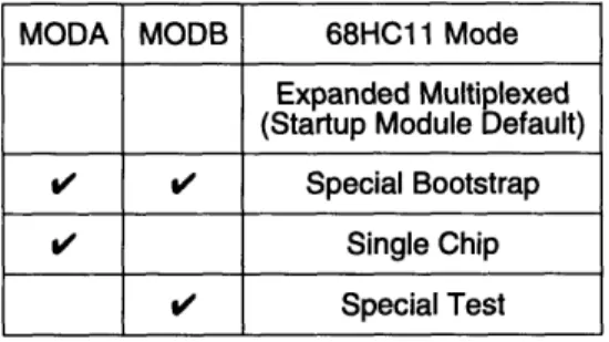
Hardware Mode Selector
The 68HC ll1 reserves two pins for mode selection during reset [4].
Nor-mally, the startup module operates with both of these pins high, enabling the
expanded multiplexed mode. However, if it becomes necessary to debug soft-ware or change the configuration of the 68HC11, it may be helpful to use one
of the special modes. As a result, jumpers are included to provide access to the special modes. Table 1 shows which modes are activated with each
jumper combination.
Table 1: Jumpers for Hardware Mode Selection
MODA MODB 68HC11 Mode
Expanded Multiplexed (Startup Module Default)
V v' Special Bootstrap
SV Single Chip
V Special Test
Power Supply Controller
The startup module is also the ideal location to place the Alewife power supply controller. The power supply can be observed and controlled using six signals. There is no external logic needed for decoding these signals so the remainder of the system can be implemented in software for the 68HC 11. The
connector for the power supply controller is provided on the board.
Analog Applications
Port E of the 68HCll is capable of capturing analog information. By
using latches to extend the output capabilities of the 68HC11, it has allowed
Port E to be reserved for analog applications. Potential applications such as
temperature sensing can be useful in examining real-world aspects of the
Board Design and Layout
The final design for the startup module was built on a four-layer board. Two layers were used as power planes, leaving two for use in routing. One power plane was used for ground and the other plane was shared by both +5 V and -5 V. The ECL parts in the clock synthesizer which required -5 V were placed in a cluster, allowing the use of a small portion of the plane as the -5 V supply. The remainder of the plane was used for +5 V.
In addition to the circuitry for the startup engine and the startup
mod-ule, extra connectors were included to support the power supply controller and P6rt E of the 68HC11. A large prototype area was also included on the board in case any additional circuitry is necessary. A picture of the assembled board is shown in Figure 3-5.
Chapter 4
Software Design & Implementation
The software for the startup module consists of several major routines. First, the setup routine initializes the 68HC 11, I/O ports, and variables for the other routines. Then, there are two independent controls for the startup
engine and the clock synthesizer. A flow chart of the software is shown in Fig-ure 4-1. The actual code implemented for the startup module is included in
Appendix C.
Global Setup
The setup routine prepares the 68HCll for operation of both the star-tup engine and the clock synthesizer. Its primary purpose is to prepare the serial ports, set defaults for the startup engine, enable the proper I/O ports, and initialize the clock synthesizer to its default frequency.
The serial ports are initialized by setting the appropriate bits in the registers which control them. Features such as baud rate can be adjusted to allow optimal performance of the serial interface.
There are only two defaults for the startup engine. These are the X and Y offsets designating the target node for the data transfer. The default is for the offsets to be zero, thus sending the startup information to the node which
Figure 4-1: Software Flow Chart
Certain I/O ports need to be reconfigured from their default operation in order to perform as desired. This is usually the case where a particular pin can act as both an input and output. Changing parameters in the control reg-isters allow the reconfiguration.
As the final setup procedure, the clock synthesizer is initialized with its default frequency. There are three variables which control the performance of the PLL. Two of these values remain constant throughout the operation of the synthesizer. The third is varied to adjust the frequency of the system. In
addition to the PLL control, the signal controlling the multiplexer is also
Startup Engine
The software design for the startup engine involves the implementation
of the EMRC protocol. In addition, it includes the development of a standard technique for utilizing the output latches residing on the data bus.
The EMRC protocol calls for a simple handshaking protocol. The
star-tup engine toggles the request line and the EMRC responds with the
acknowl-edge line. The data to be transferred should be in the EMRC latch before the
request signal is toggled. On the final byte to be transferred, the tail bit should be set. This signals the EMRC that the transfer is complete and the
next request will be the beginning of a new packet.
The request and acknowledge lines are active on each transition,
mean-ing that a change from low to high is a trigger, as well as a change from high
to low. This saves time in the handshaking, but it complicates the code a little since the behavior of the instruction set routines used need two separate blocks to handle each direction of the signal transition.
The transfer of data begins with a few standard values. These include the X and Y offsets which determine the target node for the transfer in addi-tion to the standard header and initial address for the node. This informaaddi-tion is then followed by the startup information stored in the EEPROM beginning
at location 0x1050. The X and Y offsets are both initialized to zero by the
setup routine, but can be changed when using the restart function.
This hardware implementation of the startup engine is essentially use-less if a good methodology cannot be developed for using the output latches.
The latches are triggered during a store operation to particular addresses by the 68HCll. Data for the store operation is visible on the data bus when the
address being accessed is not considered an internal address such as RAM or
registers. On writes to internal addresses, the values on the data bus are con-sidered invalid. Therefore, the latches are only useful for capturing data on external address values.
In the implementation, the latches are triggered based on two address bits, the R/W signal, and the E clock. The two address bits are A15 and A13, both in the higher eight bits of address so they are not related to internal addresses. The latch for the EMRC data triggers when A15 is high and A13 is low. The other latch, used for supplemental outputs like LEDs and the EMRC tail bit, is triggered when both A15 and A13 are high. In order to generate these bit patterns, the EMRC data latch can be considered to be at the OxD000
location in memory and the supplemental latch is considered to be at OxF000.
Of course, any addresses with the same values for A15 and A13 will work. In addition to the address bits, the latch triggers are active only when the E clock is high and the R/W signal is low. A high E clock represents the data portion of the cycle and the low R/W signal signifies a write operation.
Clock Synthesizer
The core of the clock synthesizer routine is a loop which waits for serial
input from the RS-232 port. Input can come in many forms as described in
an interactive user and used mainly for debugging purposes. The other is
intended for software control from a host computer and does not provide feed-back.
Table 2: Startup Module Control Keys
Key(s) Effect
= Echo Frequency + Increment 1 MHz
- Decrement 1 MHz
1-8 Frequency = <Input> X 10 MHz
Captures next 24 bits defining the new clock frequency Captures following two bytes as
X & Y offsets for Alewife reset
The user functions include displaying the current frequency, changing
the frequency to a multiple of 10 MHz, incrementing the frequency by 1 MHz, and decrementing the frequency by 1 MHz. Each of these operations echoes
the frequency to the RS-232 port for display on the user's terminal.
The host functions are less interactive and provide more control over the system. The load routine allows the host to load a 16-bit value into the
145170 control register. The load routine first loads an 8-bit flag to check if the clock signal selected should be in the 5 MHz to 20 MHz range or the 20 MHz to 80 MHz range. When the clock synthesizer is in the 20 MHz to 80
MHz range, the 16-bit value is directly related to the actual clock frequency. The other host function is not directly related to the clock synthesizer, but is a useful addition to the software control. It allows the host to restart
not cause the clock synthesizer to reset. By redefining the X and Y offsets, it is possible to startup the machine beginning with a different node.
One important aspect of the clock synthesizer is its smooth switching when changing frequencies. However, it is not as smooth when switching
from frequencies in the 5 MHz to 20 MHz range to ones in the 20 MHz to 80 MHz range. In order to guarantee a safe frequency switch, it is necessary to
make some software adjustments. The primary concern when switching fre-quencies is a momentary glitch when the clock becomes much faster than
expected. In this case, it can be resolved by forcing the clock to be much
slower while adjustments are made and then placing the clock at its new
fre-quency.
The situation is most easily seen when switching from a 19 MHz to 20 MHz clock. The 19 MHz clock is generated using a 76 MHz PLL signal which is divided by four. The 20 MHz clock is generated directly by the PLL, and its divide-by-four counterpart is only 5 MHz. The PLL signals and their
associ-ated divide-by-four signals are multiplexed together to select the proper signal
for the clock. In the transition from 19 MHz to 20 MHz, the 76 MHz PLL sig-nal is enabled by the multiplexer before the transition to 20 MHz has begun.
This is a problem especially when the devices using the clock are not able to handle it.
The solution is to force the multiplexer to select the slow signal while changes to the PLL are made. In addition, a short delay is required after changes are made to allow the PLL time to lock in the new frequency. Then,
the multiplexer can be set to select the proper signal for the clock. This
guar-antees the switch from 19 MHz to 20 MHz will actually change to 5 MHz before becoming 20 MHz. Changes from 20 MHz to 19 MHz will first slow to 5 MHz and then increase to 19 MHz. Finally, changes from 20 MHz to 21 MHz will slow to 5 MHz before increasing to 5.25 MHz and then 21 MHz. The
slower clock signal during the transition period does not have any negative
Chapter 5
Testing
Startup Engine
The startup engine was tested by attempting to download a simple
piece of code to an Alewife node. The code causes the node's display to cycle through the hexadecimal numbers. Successful execution of the code is suffi-cient to fully test the startup engine. Of course, several obstacles were
encountered in the process of testing.
The main problem involved the use of the output latches connected to
the data bus. Apparently, the latches were not loading the proper values. Through further testing, it appeared the latches were capturing the lower address bits of the next bus operation. The problem was solved when the trig-ger signal was modified to include the E clock, guaranteeing the trigtrig-ger would complete while data is still valid. The original trigger did not include the E clock and apparently remained active until the beginning of the next bus
cycle.
The other problem is related specifically to the EMRC latch. In the
ini-tial hardware implementation, only one address line is used to control the
triggers for the two latches. However, it is not sufficient to use only one
address bit to select the proper latch since writes to internal addresses are
vis-ible externally. As a result, an additional address line is required for decoding
are loaded into the proper latches each time and avoiding all potential con-flicts with internal addresses.
Clock Synthesizer
Testing for the clock synthesizer was conducted by attaching the output signals with an oscilloscope and verifying that the signal satisfied the pECL voltage characteristics. In addition, the exact frequency of the signal is
com-pared to the frequency set by the 68HCll to verify its accuracy. A couple
problems were encountered in the testing.
One ECL logic problem in the clock synthesizer was discovered during testing. The problem was the absence of the 5 MHz to 20 MHz clock. The
cause was traced back to an error in wiring the 10136 counter. The carry-in of
the device should have been connected to -5 V instead of ground to enable the
counter to count continuously. Instead, by grounding the input, the counter
had been configured to count once and stop.
In addition to the ECL logic problem, the PLL experienced some
prob-lems relating to jitter and time-to-lock. The original circuit implemented
would not lock to any frequency. The parameters chosen were aimed at
mini-mizing jitter, but the resulting time-to-lock was too large. After selecting new parameters and recalculating component values, time-to-lock is no longer an issue. Unfortunately, the solution to the locking problem is causing the PLL to jitter at certain frequencies. The jitter is most noticeable around 70 MHz and is also slightly visible at 27 MHz. Another evaluation of the PLL
parame-ters is necessary to find the best compromise between the time-to-lock and jit-ter problems.
Chapter 6
Startup Module Operation
The original intention of the startup module is to be able to startup the
Alewife machine independently. This implementation realizes its goal. When power is first applied to the system, the 68HCll comes out of reset after a slight delay and establishes a default clock frequency. The startup module then pauses approximately one second to allow the Alewife machine to
stabi-lize before attempting communication with the nodes. The startup engine
then begins to transfer the startup information to the Alewife node.
After the transfer is complete, the startup module contains the ability to change the clock frequency and restart the machine. In most cases, there will be a host machine connected to the startup module via the RS-232 port.
The host has precise control of the clock frequency and can also restart the Alewife machine using a particular node. In addition, the clock frequency can be adjusted by a user from a terminal using only a few keystrokes. The
con-trol is not as precise as that of the host interface, but it is sufficient for simple testing.
Chapter 7
Conclusion
Summary
The startup module satisfies the goal of being a stand-alone unit to startup the Alewife machine. Together with a fully functional SCSI node, the
VME interface will no longer be necessary. In addition, the frequency range of
the clock synthesizer provides a much wider and more useful range for testing
the Alewife prototype. This allows for the low-speed examination of some of
the details of the Alewife architecture.
Future Work
There are many areas in which the functionality of the startup module, and the environment it supports, can be explored further. The immediate future is the development of the hardware interfaces already built into the startup module such as the power supply controller and the analog port of the
68HC11. The power supply controller can be completely implemented in
soft-ware for the 68HC11. In addition, many analog applications can be developed using Port E of the 68HC11. A prototype area was included on the startup
module for the development of new hardware and the 68HCll includes many
functions designed for the analog interface.
There are also many issues to be examined for the long-term future of the Alewife machine. Some of these include the reliability of the startup
mod-ule, a redesigned startup sequence to take advantage of the startup module
Appendix A
File: startup.abl
nmodule startup
title 'Startup Module PAL'
startup device 'p22v10'; "Inputs e reset_cir ra4, runa5 adrl3, adrl5,, r_w pin pin pin pin 'Outputs run_pal r_pal rom_oe wi_e out_e reset 1; 2; 3,4; 10,11,13; pin 14; pin 15; pin 16; pin 17; pin 18; pin 19; equations _reset = reset_cir;
out_e = adr13 & adrl5 & !r_w & e; wi_e = !adrl3 & adr15 & !r_w & e; rom_oe = !(rw & e);
rpal = !ra4; run_pal = !runa5;
Appendix B
Phase-Locked Loop Design Calculations
1. Choose fref = 2 KHz
This provides good signal resolution
2. Nmax = fmax / fref = 80 MHz /2 KHz = 40000 Nmin = fmin / fref = 20 MHz /2 KHz = 10000
3. Choose = 2.0
The recommended is 0.5, but to minimize jitter, 2.0 is used.
4. (on = (Ont / t = 3.0 / 0.01 s = 300 rad/s
This for a lock-time of 10 ms.
5. K = 0.8 V/rad
Kvco = 5.26E7 rad/s/V
C = 0.8 X 5.26E7 / 40000 / 300 / 300 / 540000 = 0.021 RtF Guess R1 is 540 K12 (same as original)
Closest C is 0.01 RF
6.. R2 = 2min / (nC = 4 / 300 / 0.01E-6 = 1.33 MQ
Closest value available is 1 MQ2
Values Used in Implementation
R1 = 540 KQ
R2 = 1 MQ C = 0.01 tF
Appendix C
File: startup.azm
! startup.azm: startup module
! [email protected] .inc define .ent FFFEh .word code vector data saved_N slow_clock X_offset Y_offset print_templ print_temp2 code .ent .word .byte .byte .byte .word .byte .ent lds jsr jsr 0000h FFFFh ! Include define.azm ! Reset Vector -> 0200h
! Data at bottom of RAM
! FFFFh for Data I/O Sanity ! Flag for Slow Clock
! X Offset for Alewife Reset ! Y Offset for Alewife Reset
! Temp Storage for printN
! Temp Storage for print_N
0200h 01FFh setup engine
! The Real Thing...
i Stack Pointer at top of RAM ! Setup Ports & Stuff
! Startup Engine ! Clock Synthesizer clock ldd pshd ldx jsr cmpa beq cmpa beq cmpa beq cmpa beq cmpa beq cmpa beq cmpa blo cmpa bls _bogus ldaa jsr ldaa jsr clock 1000h input_serial RESTART_CODE _restart_ptr PRINT_CODE _printf_ptr LOAD_CODE _load_clk UP_CODE _up_clk DOWN_CODE _down_clk '1' _ten mhz '2' _bogus '8' _num mhz ' output_serial CR outputserial
ldaa LF imp output_serial _restart ptr _printf_ptr _load clk _slow_set _load _tenmhzldab imp _restart jmp _printf jsr cmpa beq ldab stab bra ldab stab jsr tab jsr bra 01h stab ldaa bra input_serial SLOWCODE _slow_set 00h (slow_clock) load 01h (slowclock) input_serial ! Load Flag
! Load 16-bit value
input_serial _update_clk
! Select slow signal of 40 MHz PLL (slow_clock)
'4' calc_N
00h
(slow_clock)
'0' ! Calculate N for new frequency
20 250 _updateclk _upc 1k _upmore ldd addd brclr addd cpd blo ldab stab ldd cpd bhi bra _dowrnclk ldd addd brclr addd cpd blo bra _down_more cpd bhs (saved_N) 500 (x + PORTA), 1500 high_N _up_more 00h (slowclock) low N highN bogus _update_clk (savedN) -500 (x + PORTA), -1500 low N _bogus _update_clk low N _update_clk ! Increment 1 MHz CLK_MASK, _upmore
! In the Slow Zone
! 20 MHz
! Decrement 1 MHz
CLKMASK, _down more
! In the Slow Zone _num._mhz _cllc N ldab stab suba tab ldaa mul ldaa mul bra
stab (slow_clock) ldd high_N - 2000 _update_clk _update_wait _printf bset std jsr ldy dey bne ldab cmpb beq bclr (x + PORTA), CLK_MASK (saved_N) write_N 1000h _update_wait (slow_clock) Olh _printf (x + PORTA), CLK_MASK
! Update PLL and Echo Frequency
ldd (saved_N) jmp print_N input_serial (X_offset) input_serial (Y_offset) engine ! Restart Alewife
! Store New Offsets
! Use Startup Engine
! Setup Startup Module
ldx 1000h ldaa staa ldaa staa ldaa staa ldaa staa ldaa staa
! X points at the registers
BAUD_SETUP (x + BAUD) SCCR2_SETUP (x + SCCR2) 2Fh (x + PORTD) DDRD_SETUP (x + DDRD) SPCR_SETUP (x + SPCR) ldaa PACTL_SETUP staa (x + PACTL) ! Serial Setup ! Port A Setup
! Set Default X & Y Offsets
! for Alewife Startup
ldaa Oh
staa (slow_clock)
bset (x + PORTA), CLK_MASK clrb jsr write_C ldd OFAOh jsr write_R ldd DEFF * 500 std (saved_N) jsr write_N bclr (x + PORTA), CLK_MASK rts
! Slow Clock Flag
! PLL Initialization ! Default Frequency ! 19 MHz _restart jsr staa jsr staa jmp setup ldaa staa ldaa staa DEFXOFF (X_offset) DEFY OFF (Y_offset)
! SPI Routines for MC145170
write_R bclr (x + PORTD), SS_MASK clr (x + SPDR)
_wait brclr (x + SPSR), 80h, _wait
write_N bclr (x + PORTD), SS_MASK staa (x + SPDR)
_wait brclr (x + SPSR), 80h, wait
write_C bclr (x + PORTD), SS_MASK stab (x + SPDR)
wait brclr (x + SPSR), 80h, wait
bset (x + PORTD), SS_MASK rts
Serial Port Routines
inDut_serial brclr (x + SCSR), 20h, input ldaa (x + SCDR) rts output_serial psha _loop ldaa (SCSR) anda 80h beq _loop pula staa (SCDR) rts
print_N brclr (x + PORTA), CLK_MASK, ldx 2000 bra _print_more _pr int_fast ldx 500 print_more idiv std (print_templ) ldaa 1 staa (print_temp2) bsr putdec ldaa jsr output serial ldd (print_templ) addd (print_templ) addd 1000 xgdx clr (print_temp2) bsr putdec ldy _print_units bsr puts ldaa CR jsr output serial ldaa LF jmp output_serial ! assert SS*
! wait for SPIF
! assert SS*
! wait for SPIF
! assert SS*
! wait for SPIF
! deassert SS*
_serial
_print_fast
! Compute MHz for Slow
! Compute MHz for Fast
! Save Remainder ! Leading Digit ' Print Quotient ! Retrieve Remainder ! Multiply by 2 ! 3 digits ! Print Remainder ! Load "MHz" ! Print Units
.asciz " MHz" 10 0 _leading putdec '0' output_serial (print_temp2) _print (Y) _exit_puts output_serial puts ! Send Character _exit_putsrts ! Startup Engine
engine bclr (x + PORTA), WIR_MASK! Clear WIR
ldy FFFFh ! Wait 1 Second for
rwaitl dey I Alewife Power-On
bne _rwaitl
ldy FFFFh ! Each Loop = 0.2 s _rwait2 FFFFh _rwait3 FFFFh _rwait4 FFFFh _rwait5 (x + PORTA), 0200h _rloopl (x + PORTA), 0200h MRC R MASK MRC R MASK ! Send Reset ! Clear Reset _rloop2 ldaa 00h staa (OUTLATCH) (X_offset) (MRC_LATCH)
(x + PORTA), WIR MASK
! Send X Offset putdec __print _leading xgdx .ldx idiv cpx beq pshb bsr pulb ldaa aba jmp ldaa bne rts put s ldaa beq iny jsr bra _rwait2 _rwait3 _nait4 _:ra it5 dey bne ldy dey bne ldy dey bne ldy dey bne __rloopl _rloop2 bset ldy dey bne bclr ldy dey bne ldaa staa bset ! Clear WIT _print_units
brclr (x + PORTA), WIA_MASK, _xwait ldaa staa bclr brset (Y_offset) (MRC_LATCH) (x + PORTA), (x + PORTA), ldy base_ROM cpy high_ROM beq _tail ldaa (y) staa (MRC_LATCH) brclr (x + PORTA), ! Send Y Offset WIR_MASK
WIA MASK, _ywait
! Send Startup Data
! Initial Location = base_ROM ! Branch tail on Last Location
WIR_MASK, _rlow _rhigh bclr _:rhigh_wia brset bra (x + PORTA), (x + PORTA), _wia
WIR_MASK ! If WIR High, Change to Low WIA_MASK, _rhigh_wia
bset (x + PORTA), WIR_MASK ! If WIR Low, Change to High brclr (x + PORTA), WIA_MASK, _rlow_wia
iny ! Next Location
bra _eloop (MRC_LATCH) WIT_CODE_HIGH (OUT LATCH) (x + PORTA), ! Last Location ! Set WIT
WIR MASK, _trlow
t _rhigh _t_rhigh_wia bclr brset bra (x + PORTA), (x + PORTA), _tail_end
WIR_MASK ! If WIR High, Change to Low WIA_MASK, _t rhigh_wia
bset (x + PORTA), WIR_MASK ! If WIR Low, Change to High brclr (x + PORTA), WIA_MASK, _t_rlow_wia
WIT_CODELOW
(OUT LATCH)
! Clear WIT
! Reset Complete
! Header for Alewife Startup
.ent 1040h .long 42941200h .long 00030000h .long 0 .long 0 ! BOOTHEADER ! BOOTADDR ! Boot Offset ! Padding
i Code should start at 1050h _ywait _e:loop _:r:Low _rlow_wia _wia tail staa ldaa staa brclr t: rLow t rLow_wia
t:ail _end ldaa staa rts
boc t _xwait
File: define.azm
! define.azm: definitions
for startup.azm
! Port A Inputs
WIA_MASK .equ 80h ! West In Acknowledge ! Port A Outputs CLK_MASK MRC R MASK WIR_MASK .equ 08h .equ 10h .equ 40h
! Clock Slow / Clock Fast *
! Alewife Reset ! West In Request ! Latch Outputs WIT_CODE_LOW .equ WIT_CODE_HIGH .equ 18h 19h
! West In Tail Low
! West In Tail High ! Clock Control LOAD_CODE SLOW_CODE UP_CODE DOWN_CODE RESTART_CODE PRINT_CODE DEF_F low_N high_N .equ .equ .equ .equ .equ .equ .equ .equ .equ 'X' 's' \+1 'r' \=, 30 10000 40000
! Load 24 bits (SLOW + 16 bits N)
! For LOAD_CODE
! Up 1 MHz ! Down 1 MHz
! Restart (16 bits for offsets) ! Print Frequency to Serial Port
! Default Frequency ! N minimum ! N maximum ! Latch Control .equ D000h .equ F000h ! MRC Latch Address ! Output Latch Address ! Port A Control
PACTL_SETUP .equ 08h ! Direction of PA3 = Output
! Serial Control SS_MASK BAUD_SETUP DDRD_SETUP SCCR2_SETUP SPCR_SETUP .equ .equ .equ .equ .equ 20h 30h 3ah Och 5ch
! bit-5 is used as an output ! /13 and /1 = 9600 8MHz in ! SPI and SCI set up.
! changed cpol to 1
! Startup Engine Control
.equ 1040h .equ 203Fh .equ 0 .equ 0
! Base Address of Boot ROM ! High Address of Boot ROM
! Default X Offset ! Default Y Offset MRC_LATCH OUTLATCH base_ROM high_ROM DEF X OFF DEFY OFF
File: init.azm
! init.azm: definitions for MC68HCllE1 ' HC11 control/status register definitions:
REG_BASE PORTA PIOC PORTC PORTB PORTCL DDRC PORTD DDRD PORTE CFORC OC1M OC1D TCNT TIC1 TIC2 TIC3 TOC1 TOC2 TOC3 TOC4 TIC4 TOC5 TCTL1 TCTL2 TMSK1 TFLG1 TMSK2 TFLG2 PACTL PACNT SPCR SPSR SPDR BAUD SCCR1 SCCR2 SCSR SCDR ADCTL ADR1 ADR2 ADR3 ADR4 BPROT OPTION .ent .byte .blkb .byte .byte .byte .byte .blkb .byte .byte .byte .byte .byte .byte .byte .word .word .word .word .word .word .word .word .word .byte .byte .byte .byte .byte .byte .byte .byte .byte .byte .byte .byte .byte .byte .byte .byte .byte .byte .byte .byte .byte .byte .blkb .byte ! start of registers 01000h 1 1 3 ! reserved ! reserved ! synonym ! reserved
! character definitions
! XON (^Q)
! XOFF (S)
! abort input line (^X) ! abort input expression (^G) ! recover from infinite loops (^C) ! restart user system (^Y)
! end-of-file for host (^D)
! CR/LF ! double quote ! single quote ! handy definitions .macro pshd pshb psha .endm .macro puld pula pulb .endm ! low-order, high-address PPROG HPRIO INIT TEST1 CONFIG .byte .byte .byte , .byte .byte XON XOFF LINEABORT SYNCABORT ASYNCABORT HARDABORT EOF TAB SPACE CR LF BS DEL EOL QUOTE SQUOTE LPAREN RPAREN DOT 11H 13H 18H 7 3 19H 4 9 32 13 10 8 7FH OAODH 34 39 (I .equ .equ .equ .equ .equ .equ .equ .equ .equ .equ .equ .equ .equ .equ .equ .equ .equ .equ .equ NIL .equ 0
References
1 Agarwal, Anant, David Chaiken, Godfrey D'Souza, Kirk Johnson, David Kranz, John Kubiatowicz, Kiyoshi Kurihara, Beng-Hong Lim, Gino Maa,
Dan Nussbaum, Mike Parkin, and Donald Yeung. The MITAlewife Machine: A Large-Scale Distributed Memory Multiprocessor.
Cam-bridge, MA: Laboratory for Computer Science, Massachusetts Institute of Technology, 1991.
2 Second-Generation Multicomputer Mesh Routing Chip (MRC). Pasa-dena, CA: Submicron Systems Architecture Project, Department of
Computer Science, California Institute of Technology, 1992.
3 Muntz, Gary. Alewife Clock Synthesizer Design. Cambridge, MA: Labo-ratory for Computer Science, Massachusetts Institute of Technology,
1993.
4 M68HC11 Reference Manual. Rev. 3. Motorola, Inc., 1991
5 MC68HC11E9 HCMOS Microcontroller Unit. Motorola, Inc., 1991.
6 CMOS Application-Specific Standard Digital-Analog Integrated
Cir-cuits. Third Printing. Motorola, Inc., 1991.
7 MECL Integrated Circuits. 4th ed. Motorola, Inc., 1989.
8 ECL Logic and Memory Data Book. Hitachi America Ltd., 1985.
9 The 41 Series of High-Performance Line Drivers, Receivers, and
Trans-ceivers - Data Book and Designers Guide. AT&T Microelectronics, 1991.
10 Power IC's Databook. National Semiconductor, Inc., 1993.