A Boundary Element Method with Surface
Conductive Absorbers for 3-D Analysis of
Nanophotonics
by
Lei Zhang
B.Eng., Electrical Engineering, University of Science and Technology of China (2003) M.Eng., Electrical Engineering, National University of Singapore (2005)
M.S., Computation for Design and Optimization, Massachusetts Institute of Technology (2007)
Submitted to the
Department of Electrical Engineering and Computer Science
in partial fulfillment of the requirements for the degree of
Doctor of Philosophy in Electrical Engineering and Computer Science
at the
MASSACHUSETTS INSTITUTE OF TECHNOLOGY
September 2010
@
Massachusetts Institute of Technology 2010. All rights reserved.
ARCHIVES
Author ...
Depp3tment of
Certified by.
Certified by.
Accepted by
...-...
Electrical Engineering and Computer Science
June 30, 2010
Jacob K. White
Electrical Engineering and Computer Science
f
A,
Thesis Supervisor
C-Ass
Steven G. Johnson
)ciate Professor of Mathematics
7; 1,
Thesis Supervisor
Terry P. Orlando
Chair, Department Committee on Graduate Students
OCrT
3
5
2
rO
A Boundary Element Method with Surface Conductive
Absorbers for 3-D Analysis of Nanophotonics
by
Lei Zhang
Submitted to the Department of Electrical Engineering and Computer Science on June 30, 2010, in partial fulfillment of the
requirements for the degree of
Doctor of Philosophy in Electrical Engineering and Computer Science
Abstract
Fast surface integral equation (SIE) solvers seem to be ideal approaches for simulating 3-D nanophotonic devices, as these devices generate fields both in an interior channel and in the infinite exterior domain. However, many devices of interest, such as optical couplers, have channels that cannot be terminated without generating reflections. Generating absorbers for these channels is a new problem for SIE methods, as the methods were initially developed for problems with finite surfaces.
In this thesis, we show that the obvious approach for eliminating reflections, mak-ing the channel mildly conductive outside the domain of interest, is inaccurate. We propose a new method in which the absorber has gradually increasing surface conduc-tivity; such an absorber can be easily incorporated in fast integral equation solvers. We present two types of PMCHW-based formulations to incorporate the surface con-ductivity into the SIE method. The accuracy of the two-type formulations are exam-ined and discussed using an example of the scattering of a Mie sphere with surface conductivities. Moreover, we implement two different FFT-accelerated algorithms for the periodic non-absorbing region and the non-periodic absorbing region.
In addition, we use perturbation theory and Poynting's theorem, respectively, to calculate the field decay rate due to the surface conductivity. We show a saturation phenomenon when the electrical surface conductivity is large. However, we show that the saturation is not a problem for the surface absorber since the absorber typically operates in a small surface conductivity regime.
We demonstrate the effectiveness of the surface conductive absorber by truncating a rectangular waveguide channel. Numerical results show that this new method is orders of magnitude more effective than a volume absorber. We also show that the transition reflection decreases in a power law with increasing the absorber length.
We further apply the surface conductive absorber to terminate a waveguide with period-a sinusoidally corrugated sidewalls. We show that a surface absorber that can perform well when the periodic waveguide system is excited with a large group-velocity mode may fail when excited with a smaller group-group-velocity mode, and give an asymptotic relation between the surface absorber length, transition reflections and
group velocity. Numerical results are given to validate the asymptotic prediction. Thesis Supervisor: Jacob K. White
Title: Professor of Electrical Engineering and Computer Science Thesis Supervisor: Steven G. Johnson
Acknowledgments
I would like to take this chance to thank my supervisor, Prof. Jacob K. White. He brought me to this great school in 2005, patiently helped me find my research direction, enlightened me through numerous discussions, and offered me freedom to pursue what I am interested. My sincere appreciation also goes to my co-supervisor Prof. Steven G. Johnson. He is a talented young scientist. His passion in research encourages everyone working with him. I learned everything about nanophotonics from him. He generously proposes his ideas through our discussions, and many ideas in this thesis came from him.
Many thanks should go to members in the Computational Prototyping group. Because of these wonderful colleagues, I really enjoyed working in this group for the five years. I would like to thank Prof. Luca Daniel, for his support and serving as my thesis committee member. I would like to thank our group assistant Chad Collins, who efficiently takes care of all executive stuff in our group. Then I would like to thank my amazing groupmates that includes my five-year officemate Bo Kim, Amit Hockman, Jung Hoon Lee, Brad Bond, Kin Sou, Tarek Moselhy, Homer Reid, Yu-Chung Hsiao, Dmitry Vasilyev, Zohaib Mahmood, Yan Zhao, Kai Pan, Laura Proctor and Steven Leibman.
I also would like to thank Ardavan Oskooi. Part of his thesis is on adiabatic absorber, based on which I worked on the analogue of the idea using surface integral equation method. I spent a summer as an intern in Ansoft Corp., I would like to thank my supervisor there, Dr. Istvan Bardi. I spent another summer in Schlumberger Doll Research in Cambridge, working on inverse algorithms. I would like to thank my advisor Dr. Aria Abubakar, and my friends there, Maokun Li, Jianguo Liu, Lin Liang, and Jiaqi Yang.
The last but not the least, actually the most important, my great thanks go to my beloved wife Yan Li and my parents. Yan and I have been married for nearly four years. I would like to thank for her generous support and care during my study. She is also a PhD student at MIT, I would like to wish her good luck next year to get her
PhD degree. I would like to greatly thank my parents for bringing me to this world, bringing me up, educating me with all their love. I am proud of you two, and I have done and will do my best to let you be proud of me.
Contents
1 Introduction
1.1 Terminating Waveguide Channels with BEM . . . . 1.2 Integral Equation Method . . . . 1.3 T hesis O utline . . . .
2 Background
2.1 Absorbers and Reflections . . . . 2.2 PMCHW formulation and Boundary Element Method.
2.2.1 Formulations . . . . 2.2.2 Integral Operators . . . . 2.3 M ie Theory . . . .
3 BEM Formulations for Surface Conductivities
3.1 Analytical Solutions of the Scattering by a Sphere with Surface Con-ductivities . . . . 3.2 Boundary Element Method Formulations with Surface Conductivities
3.2.1 Formulation Type I based on Equivalence Principle . . . . 3.2.2 Formulation Type II based on BVP... . . . . . . . . 3.3 Numerical Results and Error Analysis . . . .
4 Surface Conductive Absorber
4.1 BEM formulations for the Surface Conductive Absorber . . . . 4.2 Solving A Linear System . . . .
29 . . . . 29 . . . . 33 . . . . 33 . . . . 35 . . . - 41
4.2.1 Construction of A Linear System . . . . 76
4.2.2 Acceleration and Preconditioning with FFT . . . . 78
4.3 Numerical Results of Absorbers . . . . 80
4.3.1 Volume Conductive Absorbers . . . . 80
4.3.2 Surface Conductive Absorbers . . . . 82
4.4 The Field Decay Rate Due to the Electrical Surface Conductivity . . 84
4.4.1 Decay rate calculation by perturbation theory . . . . 87
4.4.2 Decay rate calculation using Poynting's theorem . . . . 90
4.5 Asymptotic Convergence of Transition Reflections . . . . 92
4.6 Radiation in the surface absorber . . . . 93
4.7 Electrical and Magnetic Surface Conductivities . . . . 96
4.7.1 BEM Formulations . . . . 98
4.7.2 Numerical Results and Analysis . . . 100
5 Terminating Periodic Channels with Surface Absorbers 105 5.1 Terminating A Sinusoidal-Shape Waveguide . . . 105
5.2 Numerical Results. . . . . . . 108
5.2.1 A sine waveguide with a surface absorber attached . . . . 108
5.2.2 The absorber length versus group velocity . . . 111
6 Conclusions 117 A Gaussian Beam Generated by a Dipole in A Complex Space 119 A .1 Far Fields . . . 120
A .2 N ear Fields . . . 121
List of Figures
1-1 Schematic diagram of a photonic device with input and output waveg-uide channels, which must be truncated in a boundary element method. 20 1-2 The band diagram of a waveguide with period-a sinusoidally corrugated
sidewalls (inset), showing the frequencies of the lowest two modes for propagation constants in a period k E [0,
j].
In between the lowest two modes, there is a "band gap". The period of the waveguide is denoted by a, and c denotes the speed of light in vacuum. . . . . 211-3 A perfectly matched layer for truncating a waveguide chanel in the boundary element method. . . . . 23
2-1 Illustration of a waveguide channel truncated by an absorber. . . . . 30
2-2 An illustration of Mie scattering using the boundary element method. 33
2-3 A dielectric sphere discretized using triangle panels. . . . . 36
2-4 The nth RWG basis function [1] on a pair of triangle panels. The two triangle panels are denoted by T and T,~, respectively. The length of the common edge is denoted by
I.
pn and p; are the local vectors of the point on each triangle. . . . . 372-5 A triangle panel lying on the xy plane. Observation lines 1i and 12 are parallel to the z axis with li penetrating the panel and 12 far away from the panel. . . . . 39
2-6 Components of the vector potential A and scalar potential <b along line 1i penetrating the source triangle panel in Fig. 2-5. . . . . 39
2-7 Components of V x A and Vdb along along line 11 penetrating the source triangle panel in Fig. 2-5. . . . . 40 2-8 Components of the vector potential A and scalar potential <b along a
line 12 away from the source triangle panel in Fig. 2-5. . . . . 41 2-9 Components of V x A and V(b along line 12 away from the source
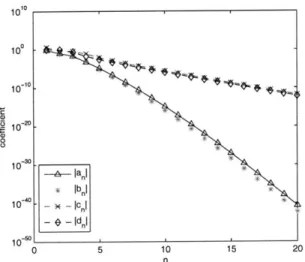
triangle panel in Fig. 2-5.... . . . . . . . . 42 2-10 The scattering of a Mie sphere. . . . . 43 2-11 The attenuation of the coefficients (2.58)-(2.61) with n of the Mie
the-ory. The radius of the sphere is 1A2, where Ai is the wavelength in the interior medium... . . . . . . . . 49
3-1 The scattering of a Mie sphere with electrical surface conductivity UE. 52 3-2 The convergence of the coefficients (3.10)-(3.13) of the Mie scattering
with surface conductivity crE = 0.01S/m. The radius of the sphere is
A... . . . . . . . . . . . . . 56
3-3 An illustration of Mie scattering with electrical surface conductivity UE using the boundary element method. . . . . 57
3-4 A discretized Mie sphere with surface conductivity UE . . . . . . .. .. 61 3-5 Comparisons of the analytical Mie solution and the two types of the
BEM formulations for calculating the magnitude of the scattered fields by a Mie sphere with surface conductivity in a polar coordinate with respect to
0.
The radius of the sphere is 1A2, and the electrical surfaceconductivity is 0.01 S. The observation circle is located at r = 2Aj, p =:r/6. . . . . 62
3-6 Comparisons of the analytical Mie solution and the two types of the BEM formulations for calculating each component of the scattered and interior fields by a Mie sphere with surface conductivity with respect to
0.
The radius of the sphere is 1A2, and the electrical surface con-ductivity is 0.01 S... . . . . . . . . . . . ... 633-7 The examination of the agreement in the equation (3.29) of the dissi-pated power on sphere surface versus surface conductivity, calculated by type I formulation. . . . . 64
3-8 Comparisons of the analytical Mie solution and the two types of the BEM for calculating the scattered and interior fields of a Mie sphere with surface conductivity, versus electrical surface conductivity
UE-The radius of the sphere is 1Aj . . . . 66
3-9 The relative error of scattered and interior fields calculated by the two
types of the BEM, versus electrical surface conductivity o-E. . . . . 67 3-10 The convergence of the magnitude of the interior field calculated by
the type II formulation, versus electrical surface conductivity o-E. The radius of the sphere is 1A. The observation point is at r = 0.6Aj, 0 = 0. 69 3-11 The convergence of the relative errors of BEM calculated interior fields
with the number of discretized triangle panels for different surface con-ductivities. . . . . 70
4-1 A discretized dielectric waveguide with an absorber attached. . . . . . 72
4-2 The 2-D longitudinal section of a waveguide with a surface conduc-tive absorber. The lengths of the waveguide and absorber are 20Aj and 10Aj, respectively, with Ai denoting the wavelength in the waveg-uide medium. The wavegwaveg-uide cross section size is 0.7211Aj x 0.7211A. The relative permittivities of the waveguide (silicon) and the external medium (air) are 11.9 and 1, respectively. . . . . 73
4-3 A discretized waveguide with a periodic unit . . . . 79
4-4 The 2-D cross section of a waveguide with a volume absorber. The lengths of the waveguide and absorber are 20Aj and 10Aj, respectively, with Ai denoting the wavelength in the waveguide medium. The waveg-uide cross section size is 0.7211A x0.7211A. The relative permittivities of the waveguide (silicon) and the external medium (air) are 11.9 and 1, respectively . . . . 81
4-5 The complex magnitude of the electric field inside a waveguide and a volume absorber of constant electrical and magnetic conductivity. The lengths of the waveguide and the volume absorber are 20Aj and 1OAj, respectively. The constant electrical volume conductivity of the volume absorber is CE = 0.0087 S/m. The dashed line indicates the position of the waveguide-absorber interface. . . . . 82 4-6 The complex magnitude of the electric field inside a waveguide and
a volume absorber of constant electrical and magnetic conductivity. The lengths of the waveguide and the volume absorber are 20Aj and 60Aj, respectively. The constant electrical volume conductivity of the volume absorber is crE = 0.0015 S/m . . . . 83
4-7 The complex magnitude of the electric field inside a waveguide and a surface absorber. The dashed line indicates the position of the waveguide-absorber interface. . . . . 85 4-8 The complex magnitude of the electric field inside a waveguide and a
surface absorber. The dashed line indicates the position of the absorber interface . . . . 86 4-9 The 2-D longitudinal section of a waveguide with uniform surface
conductivity. The waveguide length is 10Aj and cross section size is 0.7211A x 0.7211A,. The relative permittivity of the waveguide and external medium are 11.9 and 1, respectively . . . . 86 4-10 The complex magnitude of the electric field along x inside the
waveg-uide in Fig. 4-9 with uniform surface conductivity. . . . . 87 4-11 A comparison of three methods for computing the rate of field
expo-nential decay along the propagation direction versus surface conductivity. 88 4-12 Illustration of the approach using Poynting's theorem to calculate the
decay rate of a waveguide with surface conductivity. The plot of the surface conductivity distribution UE (x) along the longitudinal direction
4-13 Asymptotic power-law convergence of the transition reflection with the length of the surface absorber. The length of the waveguide is 1A, with Ai denoting the wavelength in the waveguide medium. The
waveg-uide cross section size is 0.7211Aj x0.7211Aj. The relative permittivities of the waveguide (silicon) and the external medium (air) are 11.9 and 1, respectively. . . . . . . . . .. . . 94
4-14 The complex magnitude of the electric field inside a waveguide and a long surface absorber excited by a dipole source and a Gaussian beam, respectively. The lengths of the waveguide and the absorber are 10Aj and 30Aj, respectively. The surface conductivity on the absorber increases quadratically. . . . .. . 95
4-15 The 2-D longitudinal section of a waveguide with uniform electrical and magnetic surface conductivities rE and aM. The surface conductivities satisfy aM E- The waveguide length is 8Aj and the cross section size is 0.7211A x 0.7211 A. The relative permittivities of the waveguide and external medium are 11.9 and 1, respectively. . . . . 98
4-16 The complex magnitude of the electric field along the central axis inside a waveguide with electrical and magnetic surface conductivities 0E and
aM, respectively. The surface conductivities satisfies aM - 7E. The
length of the waveguide is 8Aj. . . . . 101
4-17 The numerically measured decay rate due to the electrical and mag-netic surface conductivities versus the electrical surface conductivity. The magnetic surface conductivity scales proportional to the electrical
surface conductivity, specifically, aM - E . . .. . . . . . . . . 102
4-18 The geometry of a 1-D layered media in the z direction. The permittiv-ities and permeabilpermittiv-ities of the three region are identical, and denoted by c and p. The width of region 2 is denoted by Az. . . . . 103
5-1 A 3-D discretized sine waveguide with a surface absorber attached. The period of the waveguide is denoted by a, the length of the absorber is denoted by L, and t denotes the thickness in the z direction. The relative permittivities of the waveguide and the exterior media are 11.9 and 1, respectively. . . . 106 5-2 The 2-D longitudinal section of a sine waveguide with a surface
ab-sorber attached. The period of the sine waveguide and abab-sorber is a. The maximum and minimum sizes in the y direction are denoted by hM and hm, respectively. The dashed line indicates the interface of the waveguide and absorber. The surface conductivity on the absorber is
denoted by UE(r)- . . . . . . . .. 106
5-3 The complex magnitude of the electric field along the x-axis of a sine waveguide and a surface absorber, when the waveguide system is excited with k = 0.3042. a The conductivity-function coefficient
o =_ 0.006S. The dashed line indicates the position of the waveguide-absorber interface. . . . 109 5-4 The complex magnitude of the electric field along the x-axis of a sine
waveguide and a surface absorber, when the waveguide system is ex-cited with k = 0.436 . The conductivity-function coefficient is differ-a ent for each plot.. . . . . . . . . 110 5-5 The required surface absorber lengths and the corresponding total
re-flections for linear, quadratic and cubic conductivity profiles, as the conductivity linear factor uo is proportional to 9(d + 1). The group velocity is substituted with Ak. . . . 112 5-6 The required surface absorber lengths and the corresponding total
reflections for linear, quadratic and cubic conductivity profiles (d = 1, 2,3), as the conductivity linear factor uo is proportional to d+. The group velocity is substituted with Ak. . . . 114
A-1 Electric fields in the yz plane due to a point current source at the origin in a complex coordinate, b = 4A. . . . . 124 A-2 The electric fields at z = 0+ and z = 0- along the y axis due to a
point current source at the origin in a complex coordinate, showing the discontinuity of the electric fields across the z = 0 plane, and b = 4A. 125 A-3 Electric field in the yz plane due to a point current source at theorigin
List of Tables
3.1 The average magnitudes of the RWG-function coefficients of the un-known currents for the two types of formulations . . . . 68
4.1 The Standing wave ratio (SWR) and field reflection versus the conduc-tivity distribution of the absorber, whose length is 1A0. . . . . 84
Chapter 1
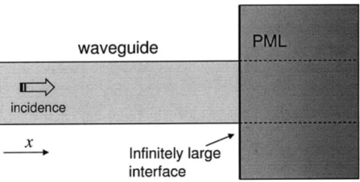
Introduction
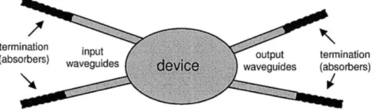
In this thesis, we describe a surface conductive absorber technique for terminating optical channels with the boundary element method, which otherwise has difficulties with waveguides and surfaces extending to infinity. In order to attenuate waves re-flected from truncated waveguides, we append a region with surface absorption to the terminations, as diagrammed in Fig. 1-1. The transition between the non-absorbing and absorbing regions will generate reflections that can be minimized by making the transition as smooth as possible. We show how this smoothness can be achieved with the surface absorber by smoothly changing integral-equation boundary condi-tions. Numerical experiments demonstrate that the reflections of our method are orders of magnitude smaller than those of straightforward approaches, for instance, adding a volume absorptivity to waveguide interior. In addition, We apply the sur-face absorber to truncate periodic waveguide channels, and show that the difficulty to eliminate transition reflections increases as the group velocity of excited modes de-creases. To solve the difficulty, we show that the absorber length should be increased, and provide asymptotic relations between absorber length and group velocity.
1.1
Terminating Waveguide Channels with BEM
Many nanophotonic devices have input/output waveguide channels to couple power/signal into and out of the device system. By introducing a periodic modulation into an
elec-tromagnetic waveguide channel, one can obtain a variety of effects useful for photonic devices [2]: periodicity creates band gaps that can be used to confine light [2], while near the edge of the gap there are "slow light" modes with a group velocity -- 0 which can increase light-matter interactions for nonlinear devices [3-5], tunable time delays [6], dispersion compensation [7-12], or other applications. The periodicity can take many forms, such as a waveguide with periodically varying width as in Fig. 1-2 (inset), waveguides with periodic holes [2], "fiber Bragg gratings" with periodic index variation [7,13], and so on. In this thesis, we consider the application of boundary element methods (BEM) [1, 14-17] to study devices incorporating waveguide chan-nels with uniform or periodic cross section. The boundary element method is a powerful computational technique because it handles homogeneous regions analyti-cally and only discretizes interfaces between materials, and no artificial truncation is needed for the infinite space surrounding a device-however, waveguide-based devices pose a challenge because the input/output waveguide surfaces must still be truncated with some artificial absorber in order to eliminate spurious reflections. In volume-discretization methods like the finite-difference time-domain (FDTD) method [18,19], one must truncate space as well as waveguides, and the traditional solution is a per-fectly matched layer (PML) [20-23], but the PML idea is based on an analytic contin-uation that is not applicable to periodic waveguides [24]. A fallback is an adiabatic absorber, in which some kind of absorption is turned on gradually in order to ab-sorb outgoing waves with minimal reflection [24]. In this thesis, we present the BEM analogue of the adiabatic absorber idea for truncating waveguides, by a gradually in-creasing surface conductivity that can be efficiently implemented with a surface-only
t na input output termination
(absorbers) waveguides device waveguides (absorbers)
Figure 1-1: Schematic diagram of a photonic device with input and output waveguide channels, which must be truncated in a boundary element method.
Ca 0.25 0.2 0.15 0.1 0' 0 0.1 0.2 0.3 0.4 0.5 0.6 0.7 0.8 0.9 1 k (2n/a)
Figure 1-2: The band diagram of a waveguide with period-a sinusoidally corrugated sidewalls (inset), showing the frequencies of the lowest two modes for propagation constants in a period k
C
[0,g].
In between the lowest two modes, there is a "band gap". The period of the waveguide is denoted by a, and c denotes the speed of light in vacuum.discretization. Moreover, we apply this technique to truncating periodic waveguides in BEM, where in this case we show that the problem becomes much more difficult in the limit of slow-light modes, due to a well-known phenomenon that transition reflections are exacerbated for slow light
[6,
24, 25]. More generally, the same tech-nique could be used for low-reflection termination of any periodic medium (photonic crystals [2]), not just waveguides.Since many nanophotonic devices consist of piecewise homogeneous materials, the boundary element method (BEM) [1, 14-17] is a popular full-wave numerical method for a general photonics solver. Unlike the difference or the finite-element volume-discretization methods, boundary finite-element methods treat infinite ho-mogeneous regions (and some other cases) analytically via Green's functions, and therefore often require no artificial truncation of space. Because BEM only requires surfaces to be discretized, they can be computationally efficient for problems involving piecewise homogeneous media, particularly since the development of fast O(NlogN) solvers [26-29]. However, a truncation difficulty arises with unbounded surfaces of
infinitely extended channels common in photonics. Fig. 1-1 is a general photonic device schematic with input and output waveguide channels. In order to accurately simulate and characterize the device, such as calculating its scattering parameters, formally, the transmission channel must be extended to infinity, requiring infinite computational resources. A more realistic option is to truncate the domain with an absorber that does not generate reflections.
The key challenge is to design an absorber that both has small reflections and is also easily incorporated into a BEM solver. The best-known absorber is a perfectly matched layer (PML) [19-23,30] as shown in Fig. 1-3. The idea behind the PML is the stretched coordinate in a complex space, so the PML should be a layer with infinitely large interface, which requires the BEM to truncate the interface. More importantly, in order to avoid discretization error, the PML should be a continuously varying anisotropic absorbing medium, whereas boundary element methods are de-signed for piecewise homogeneous media. A similar problem arises if one were to simply add some absorption within the waveguides-in order to minimize transition reflection, the absorption would need to increase gradually from zero [24], correspond-ing again to inhomogeneous media. One could also use a volume integral equation (VIE) [31] or a hybrid finite-element method in the inhomogeneous absorbing region, but then one would obtain numerical reflections from the discontinuous change in the discretization scheme from the BEM to the VIE. Moreover, it has been proposed that an integral-equation PML can be obtained by varying the Green's function instead of the media [32], but a continuously varying Green's function greatly complicates panel integrations and makes it difficult to implement a fast solver without the space-invariant property.
In this thesis, we examine an alternative approach to absorbers, adding electri-cal conductivity to the waveguide surface rather than to the volume, via a Dirac delta function conductivity on the absorber surface. The absorber's interior medium remains the same as the waveguide's, thus eliminating the need to discretize the waveguide-absorber interface. This surface-conductivity strategy permits an efficient surface-only discretization, but at the same time allows for a smoothly increasing
Figure 1-3: A perfectly matched layer for truncating a waveguide chanel in the bound-ary element method.
surface conductivity, thereby reducing transition reflections. Specifically, surface con-ductivity is easily implemented in boundary element methods as it corresponds to a jump discontinuity in the field boundary conditions at the absorber surface. Since boundary element methods explicitly discretize the surface boundary, continuously varying the field boundary conditions is easily implemented. Numerical results show that the reflections of the surface absorber can be made negligible by appropriate
taper designs.
The reflections of an absorber include a round-trip reflection and a transition reflection. The round-trip reflection is caused by the wave traveling to the end of the absorbing region and reflecting back from the end without being completely ab-sorbed, and it can be reduced by a larger absorption or a longer waveguide. The transition reflection is the immediate reflection at the waveguide-absorber interface due to the transition in medium properties. An adiabatic absorber
[24]
gradually in-creases the material absorption to reduce the transition reflection. It has been shown using coupled-mode theory[24]
that the transition reflection decreases as a power law with increasing absorber length L, and the smoothness of the conductivity profile determines the power law. Specifically, the transition reflection scales proportional to L-(2d+2) , where d is the order of the conductivity function.Bloch's theorem [2] states that the propagating modes of a periodic waveguide can be written in the form E(r) = e-i'kEk(r), where x is the wave propagation
direction, k is the propagation constant in the x direction, and Ek(r) is a periodic function with the physical period a in x. While it may not be obvious that a periodic structure supports guided modes, the periodicity implies a conserved k, which allows true guided modes to be localized below the light cone in the band diagram [2]. As an example, we consider a waveguide with sinusoidally corrugated sidewalls, described in more detail in Sec. 5.2. The dispersion relation of such a "sine waveguide" can be calculated using a planewave method [33], and the two lowest modes for propagation constants k E [0,
g]
are shown in Fig. 1-2. The frequency range between the two modes represents a band gap in the guided modes [2]. Note that the slope of the band d is the group velocity V, the velocity at which energy, information and wavepackets propagate [2]. It is obvious that the group velocity approaches to zero as the frequency approaches the band-gap edge in the diagram. And it has been shown in [24] that the transition reflection increases in a power law as the group velocity decreases. Therefore, absorbers for the periodic waveguide will experience difficulty when the waveguide system is excited at the band-gap edge. This thesis will provide guidance for increasing the length of the absorber to reduce the transition reflections when the group velocity is small.1.2
Integral Equation Method
The integral equation method is a popular full-wave method to solve Maxwell's equa-tions in frequency domain. Based on discretization schemes, it could be divided into the volume integral equation (VIE) method [31], which discretizes the whole volume of a computational domain, and the surface integral equation (SIE) method, [1,14-17], which only discretizes the interfaces of piecewise homogeneous regions and, in each homogeneous region, analytical solution can be obtained via corresponding Green's functions. For inhomogeneous medium, the volume integration method (VIE) is gen-erally chosen to use by discretizing the whole space domain and parameterizing the inhomogeneous material property, since Green's functions for inhomogeneous medium is usually difficult to obtain. For homogeneous or piecewise-homogeneous medium,
the surface integral equation method is appealing because one could simply use the homogeneous-space Green's function to make a general solver, and the surface-only discretizing scheme turns a 3-D geometry to a 2-D like surface, could significantly save computational costs.
The boundary element method (BEM) is a popular surface integral equation method, and has been developed for decades for simulating a variety of applica-tions. The boundary element method with electric-field integral equation (EFIE) or magnetic-field integral equation (MFIE) formulations could be used to analyze mi-croship antennas [34-36] based on the mixed-potential integration equation (MPIE), which yields a weaker singularity in its integrands than the single potential formula-tion. The development of the RWG functions defined on triangle panel pairs [1] offers great flexibility with non-uniform discretizations for analyzing objects with arbitrary surfaces, such as arbitrarily shaped microstrip patch antennas
[37.
With either Poggio-Miller-Chang-Harrington-Wu (PMCHW) formulation [14, 15] or combined-field integral equation (CFIE) formulations, radiation and scattering problems by 3-D penetrable dielectric bodies could be modeled with the boundary element method [14,17,38].As mentioned above, the boundary element method formulations include the EFIE, MFIE, PMCHW and CFIE [39,40]. The EFIE and MFIE are typically used to analyze geometries involving perfectly electrical conductor (PEC) or perfectly mag-netic conductor(PMC) bodies by enforcing electric field boundary condition (EFIE) or magnetic field boundary condition (MFIE) on the surfaces. However, the EFIE and MFIE could encounter singularities of the integral operators and generate spu-rious solutions when the analyzed body is exited at its resonating frequencies [14]. Instead, the PMCHW and CFIE formulations could avoid the singularity problem by enforcing both the electric and magnetic field boundary conditions at body surfaces, and are typically used to analyze dielectric bodies.
In this thesis, following the PMCHW formulation, we propose two types of bound-ary element method formulations for simulating dielectric bodies with electrical sur-face conductivities. The sursur-face conductivity corresponds to a Dirac delta function on
the surface, and hence it creates a jump for tangential magnetic fields across the sur-face. We illustrate the two types of formulations using a scattering problem [41-44] of a Mie sphere with electrical surface conductivities. The numerical BEM results of scattered and interior fields of the two formulations are compared with derived analytical solutions. For small surface conductivities, the type II solution is as ac-curate as the type I solution. For large surface conductivities, the scattered field of type II remains the same accuracy as type I, but the interior field inside the sphere has a larger error and shows a larger coefficient of its power-law convergence with discretizations. The large error occurs because the interior field becomes smaller as the surface conductivity increases. The type II formulation, therefore, has more nu-merical cancellation errors with two sets of unknown currents. However, since the interior fields are several orders of magnitudes smaller than the scattered fields when the large error occurs, the error could be numerically ignored. We further show that the cancellation error of the type II formulation will not cause numerical problem for analyzing the surface conductive absorber. For waveguide channel, the excitation source is located in the interior region, and power is localized in the waveguide inte-rior. Thus, the interior field is dominant, like the scattered field in the Mie scattering case. Also, the surface conductivity of the absorber remains small when chosen to minimize transition reflections at the waveguide-absorber interface.
The boundary element method becomes more competent for large scale simula-tions particularly since a few acceleration techniques was developed, like the precorrected-FFT (Pprecorrected-FFT) method [26-28,45-49] and the fast multipole method [29, 50]. These fast methods eliminate the need to fill and store a large full matrix. Instead, they only require storing a sparse matrix, which takes much less storage (O(N)) and computa-tional time O(NlogN). The Precorrected-FFT method was first proposed in [26,45] to solve electrostatic problems, and it has been further developed in [27,28,46-49] to solve dynamic electromagnetic problems. In this thesis, to take advantage of periodic-ity of discretized channel structures, we use a straightforward and easily-implemented FFT-based fast algorithm to accelerate the boundary element method. With this im-plementation, the solver could nearly achieve O(NlogN) computational requirement.
1.3
Thesis Outline
This thesis is organized as follows. In Chapter 2, we provide background knowledge in order for better understanding the thesis. The background includes the analysis of the reflections of generated by a general absorber for truncating a guided channel; the introduction of the PMCHW formulation, the boundary element method and
corresponding integral operators; and the derivation of Mie theory.
In Chapter 3, we describe two types of boundary element method formulations to analyze dielectric bodies with electrical surface conductivities. We illustrate the derivation of the BEM formulations as well as analytical solutions using a scattering problem of a Mie sphere with surface conductivities. Error analysis is performed to compare the two types of of formulations.
In Chapter 4, we present a surface conductive absorber technique for truncating a dielectric waveguide with uniform cross section in the simulation using the boundary element method. Numerical results show that the surface absorber generates several orders of magnitudes smaller reflections than the straightforward volume absorber. The field decay rate due to the surface conductivity is calculated using two methods. The asymptotic attenuation of the transition reflection of the surface absorber with the absorber length is examined.
In Chapter 5, we apply the surface conductive absorber technique to truncate periodic waveguide channels. We demonstrate the performance of the absorber using an example of a waveguide with period-a sinusoidally corrugated sidewalls. We show the difficulty to terminate the periodic waveguide when excited with a small group-velocity mode, and show the relation between the absorber length and group group-velocity to achieve fixed transition reflection.
Chapter 6 concludes the thesis and describes future work.
In Appendix A, we describe a Gaussian beam generated by a dipole in a complex space, which is used as an excitation throughout the thesis.
Chapter 2
Background
This chapter presents background knowledge for better understanding this thesis. Since this thesis focuses on developing a new surface conductive absorber for termi-nating waveguide channels with generating minimal reflections, this chapter begins with an introduction of a general absorber, and the round-trip reflection and the tran-sition reflections generated by the absorber. We describe formulations to evaluate the round-trip reflection and the key elements to determine the transition reflection. We briefly describe the PMCHW formulation with the boundary element method, based on which two types of formulations will be presented to incorporate surface conduc-tivities in Chapter 3. In order to benchmark the new formulations, Chapter 3 will also provide an analytical solution of the scattering by a dielectric sphere with surface conductivities, and thus in this chapter, we describe the derivation of Mie theory.
2.1
Absorbers and Reflections
A waveguide channel with a general absorber attached is illustrated in Fig. 2-1. The absorber truncates the waveguide channel by absorbing propagating waves as if the wave propagates along an infinitely long channel without any reflection. The advan-tage to attach an absorber is that an infinitely long channel can then be numerically analyzed in a finite domain using finite computational resources. An absorber is an artificial part in the whole computational domain to aid the analysis of primary
appli-waveauide
absorber
Transition
F
L
Round-trip
reflection
reflection
Figure 2-1: Illustration of a waveguide channel truncated by an absorber.
cations with infinitely extended channels, therefore, a good absorber should be small in size, and thus requiring reasonable computational power. And more importantly, it should generate small reflections within the tolerance of applications. In this sec-tion, we introduce the reflections generated by an absorber, and generally discuss the relations between the reflections and the property of the absorber including length, absorptivity and absorption profile.
As shown in Fig. 2-1, the reflections generated by an absorber can be divided into a round-trip reflection, R,, and a transition reflection, Rt. The round-trip reflection is generated by waves entering into the absorber, propagating to the end without being completely absorbed, reflected off the end of the absorber, and eventually propagating back into the waveguide. As shown in Fig. 2-1, the length of the absorber is denoted by L, wave propagates in the
+X^
direction, and the waveguide-absorber interface is located at x = xo. The round-trip reflection coefficient is proportional toRr, e-4 fL(x)dx, (2.1)
where a(x) is the field decay rate due to the absorptivity of the absorber, a factor of 2 in the exponent of (2.1) represents the effect of the round trip, and another factor of 2 indicates that the power is considered.
Consider a dth-order monomial function s(u) defined in u E [0, 1]
ud 0 < u <(
and a conductivity function of the absorber is defined with s(u)
u(X) = Uos( L ), (2.3)
where uo is the coefficient of the conductivity function. From the perturbation analysis in Sec. 4.4.1, the decay rate a (x) in (2.1) is proportional to ( 5' in the limit of small ao, where V is the group velocity of the propagating mode. Therefore, after integrating the exponent in (2.1), the round-trip reflection asymptotically attenuates with
4La0
Rr e (d+1)T. (2.4)
The round-trip reflection exponentially decays with the conductivity coefficient Oo and absorber length L, so that it can be reduced by increasing Uo or the absorber length. However, large ao will increase the transition reflection, which will be dis-cussed below. In general, the round-trip reflection is fixed with a very small value when discussing the transition reflections, and the conductivity coefficient is therefore made proportional to
Or ' (d + 1)V J~ L .(2.5) 25
The transition reflection Rt is the reflection generated by the transition in material properties at the waveguide-absorber interface. It can be analyzed using coupled-mode theory [51,52] in a slowly varying medium along propagation direction. Here we skip the analysis process, and directly provide the conclusion. In the limit of large L, the magnitude of a reflected mode Cr(L) in an asymptotic form is given [24]
cr(L) = s( (0+) M(0+) [-jLA]-d + O(L-(d+l)), (2.6)
AQ(O+)
where AO = 3 -Or is the difference between the propagation constants of the incident
and reflected modes, s(d)(0+) is the dth-order derivative of s(u) evaluated at u = 0+, and M is a coupling coefficient between the incident and reflected modes, depends on the spatial field pattern but is a smooth function of u [24, 52], and M(O+) is
asymptotically proportional to
M(0+) go (2.7)
A/3'
Therefore, the transition reflection is proportional to
Rt ~ (o- (T.Ld -Af3(d+2)) . (2.8)28
As we know, the group velocity V is proportional to A3 in the limit of small V [24), so AO can be replaced with V in (2.8).
For a single-mode excitation, the round-trip reflection could be fixed by following (2.5) as go ~ L for a same-order conductivity profile (same d). Therefore, the
transition reflection should be expected to be proportional to
1 1
Rt ~ L2d+2 * V2d+2
(2.9)
For a multiple-mode excitation, the group velocity for each mode is generally different, therefore, we are unable to strictly fix the round-trip reflection. Instead, we could conservatively fix the round-trip reflection by picking the initial go working well for the large V mode (achieving small round-trip reflection for the large V mode)
and making co inversely proportional to the absorber length as
ao
~ 1. With thischoice of
o,
the asymptotic form of the transition reflection is1 1
L2d+2 V2d+4 (2.10)
For the two choices of the conductivity coefficient
go,
the transition reflectionattenuates asymptotically in a power law with the absorber length as R ~ T-76.
The power-law behavior indicates that, with a higher-order conductivity function, the transition reflection decreases faster with increasing the absorber length. It does not follow that d should be made arbitrarily large, however, there is a tradeoff in which increasing d eventually delays the onset L of the asymptotic regime in which
| Et
Figure 2-2: An illustration of Mie scattering using the boundary element method.
(2.9) and (2.10) are valid [24]. This will be further discussed in Chapter 5 with numerical results.
2.2
PMCHW formulation and Boundary Element
Method
In this section, we briefly describe the PMCHW formulation [14,15] and the boundary element method [1,14-17] by numerically solving a Mie scattering problem, which will be analytically solved via a boundary value problem in Sec. 2.3.
2.2.1
Formulations
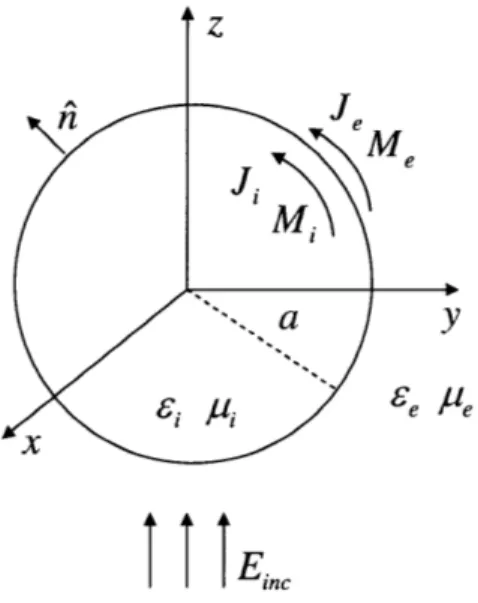
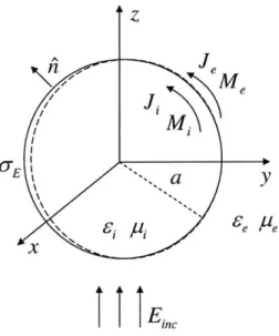
Fig. 2-2 shows a dielectric sphere embedded in an exterior medium. The radius of the sphere is denoted by a. The permittivities and permeabilities of the sphere medium
and the exterior medium are denoted by ci, pi, and e, pe, respectively. An x-polarized plane-wave propagating in the z direction shines on the sphere, and thereby generates scattered fields in the exterior region and interior fields in the sphere. The unknowns
of the BEM are equivalent electrical and magnetic currents Je, Me on the exterior side of the sphere surface, and Ji, Mi lying on the interior side of the surface, with the subscripts e and i denoting the exterior and interior side, respectively.
The scattered fields are treated as if being excited by the currents Je, Me in a homogeneous space of ee and ye (exterior problem), and the interior fields are treated as if being excited by the currents Ji, Mi in a homogeneous space of 6i and pi (interior problem). According to the equivalence principle [53,54], in order to treat the exterior or interior problem as in a homogeneous space, the following boundary conditions should be satisfied [39]
-n X [Einc + E,(Je, Me)] = Me, (2.11)
n x [Hinc + Hs(Je, Me)] = Je, (2.12)
i x Ej(Jj,Mj) = Mi, (2.13)
-nxHj(Jj,Mj) = Ji. (2.14)
where Einc and Hic are the incident electric and magnetic fields, respectively. E, (.), H, (.) are the integral operators of the electric and magnetic fields evaluated in a homogeneous space whose material property is the same as that of the exterior region, and E(-), H(-) are the integral operators evaluated in a homogeneous space whose material property is the same as that of the interior region.
nt
is the normal exterior-pointing unit vector.The boundary conditions are then enforced to couple the exterior and interior problems. Specifically, the continuity of the tangential components of the electric and magnetic fields on the sphere surface yields the PMCHW formulation
ii x [Einc + E,(Je, Me)] = X Ei(J , Mi), (2.15)
i x [Hinc + H,(Je, Me)] =
n
x Hi(Ji, Mi). (2.16)The field-continuity boundary condition provides two independent equations (2.15)-(2.16) with four unknown currents Je, Me, Ji, Mi, leaving two degrees of freedom.
Substituting the field-current relations (2.11)-(2.14) into (2.15) and (2.16) yields the relations between the currents on the exterior and interior sides. It turns out that the current on the two sides have the same magnitude and sign flipped. Therefore, the four sets of unknown currents can be reduced to two sets, J and M, by
Je = -Jj = J, (2.17)
Me = -Mj = M. (2.18)
Substituting (2.17), (2.18) into (2.15), (2.16) yields the final version of the PMCHW formulation
n
x [E,(J, M) - Ei(-J, -M)] = -n x Einc, (2.19)n
x [H,(J, M) - Hi(-J, -M)] = -n x Hinc. (2.20)The fields can be substituted by the integral operators introduced in the next section, the integral equations can then be discretized to construct a linear matrix system using the Galerkin method
[55],
and the unknown currents J and M can be determined by solving the linear system.2.2.2
Integral Operators
From Sec. 2.2.1, the two equivalent currents J and M on the sphere surface are to be determined by solving the PMCHW formulations (2.19)-(2.20). First of all, the sphere surface is discretized with triangle panels as show in Fig. 2-3, and the currents are approximated with the RWG basis function [1] on triangular-meshed surfaces as shown in Fig. 2-4, and the approximated currents become
J = JmXm(r'), (2.21)
M = MmXm(r'), (2.22)
Figure 2-3: A dielectric sphere discretized using triangle panels.
where Xm(r') is the RWG function on the mth triangle pair, and Jm, Mm are the corresponding coefficients for the electric and magnetic currents, respectively.
Electric and magnetic fields are represented using the mixed-potential integral equation (MPIE) [16] for a low-order singularity, with integral operators L and K as in [17] E1(J, M) H(J, M) = -ZL 1(J) + KI(M), = -KI(J) I Li (M), (2.23) (2.24)
where Z, = /yt/61 is the intrinsic the exterior or interior region. The are given by
Li(r, Xm(r')) J
Ki(r, Xm(r')) =
-impedance, and the subscript I = e or i denotes integral operators due to the mth RWG function
,A,(r, Xm(r')) +
V bz(r, Xm(r)),V x A,(r, Xm(r')),
(2.25) (2.26)
where r and r' are, respectively, the target and source positions and k, = ofpia- is the wavenumber. The vector and scalar potentials A, <b due to the RWG function
Figure 2-4: The nth RWG basis function [1] on a pair of triangle panels. The two triangle panels are denoted by T+ and T-, respectively. The length of the common edge is denoted by 1li. p+ and p- are the local vectors of the point on each triangle.
Xm(r') are
A(r, Xm(r')) = G1(r, r')Xm(r')dS',
<b(r, Xm(r')) = G1(r, r')V' - Xm(r')dS',
(2.27)
(2.28)
where S,, is the surface of the mth triangle pair, and Gl(r, r') is the Green's function in a homogeneous space whose material property is the same as region 1, and it is
e-jklirr'I
47rr - r'| (2.29)
When target points are far away from the source panel, the integral of (2.27) and (2.28) can be numerically calculated using Gauss quadrature [56]. For near-fields, the panel integration can be evaluated using a variety of methods [57-60].
We employ Galerkin method [55] by using the RWG function as the testing func-tion on target triangle pairs. The tested L, K operators on the nth target triangle
pair due to the mth source triangle pair become
Li,nm(Xm) =
Xn(r)
-
Li(Xm)dS,(2.30)
KCi,nm(Xm) = inX,(r) - K,(Xm)dS, (2.31)
where Sn is the surface of the nth target triangle pair. Substituting the tested field op-erators into equations (2.19)-(2.20) yields a matrix with unknown vectors of the RWG coefficients. The linear equation system can be solved either directly or iteratively.
One may notice that in (2.19), the scattered field operator E,(J, M) and the interior field operator Ei(-J, -M) take the flipped-direction input currents, but their difference should be equal to Eic rather than just a sign flipped. On physical grounds, it is clear that E, and E, can have very different magnitudes. Consider the case of identical interior and exterior media, so that there will be zero scattered field E, and the interior field E, will be the same as the incident field. However, it may not be immediately obvious how such different field magnitudes can arise in this formulation, especially for identical media, given that E,(J, M) and Ei(-J, -M) are generated by equal and opposite currents. (Note, however, that Ei is not a merely a mirror flip of E, even for identical media: due to the pseudovector nature of magnetic fields and currents [61], a mirror flip across the interface would correspond to
+J,
-M currents, or vice versa for an antimirror flip. So, flipping the sign of both currents changes E in a nonsymmetrical manner.)Here, we briefly explain how this phenomenon arises in terms of the nature of the integral operators. In particular, this phenomenon is determined by the gradient and curl operators in the integral operators L and K in (2.25)-(2.26) for the self term (target and source triangles overlap, m = n in (2.30)-(2.31)) of the system matrix.
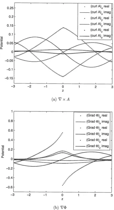
Consider a source triangle panel S' lies on the xy plane where z = 0, as shown in Fig. 2-5. Two observation lines 11 and 12 are perpendicular to the triangle panel,
and line 11 intersects with the panel but 12 doesn't. The x and y components of the vector potential A and scalar potential <b along line 11 due to the currents and charges (represented by RWG functions) on the source triangle panel is shown in Fig. 2-6.
:1
1
12
_10
Figure 2-5: A triangle panel lying on the xy plane. Observation lines
li
and 12 are parallel to the z axis with 11 penetrating the panel and 12 far away from the panel.0.4 A real 0.3 - A, imag A real . . Y 0.2- A imag .D real -e 0.1 - .D imag (L.* -3 -2 -1 0 1 2 3 z Figure 2-6: Components
11 penetrating the source
of the vector potential A and scalar potential 4 along line triangle panel in Fig. 2-5.
The potentials are symmetric with z = 0, and the real parts of the potentials A and 4 are non-differentiable with respect to z at z = 0. Therefore, the real part of z and Pt has a sign difference for z = 0+ and z = 0-. This is shown in Fig. 2-7 thataz
-3 -2 -1 0 1 2 3 z (a) V x A -0.2--0.4 --0.6 --3 -2 -1 0 1 2 3 z (b) V <1
Figure 2-7: Components of V x A and Vdb along along line 11 penetrating the source triangle panel in Fig. 2-5.
the real parts of the x and y components of V x A and the z components of V4b are discontinuous and flip signs across z = 0. This jump at z = 0 is responsible for the
in 0.05-0 a- 0--0.1 - ---...----0.05 -0.15 -3 -2 -1 0 1 2 3 Z
Figure 2-8: Components of the vector potential A and scalar potential 4 along a line
12 away from the source triangle panel in Fig. 2-5.
difference of L and K in (2.25) and (2.26) in the self term at the exterior and interior sides of the surface. The imaginary part of the self-term potentials corresponds to a sinc function, so the derivative with respect to z is the same for both the exterior and interior sides.
Figure 2-8 shows the potentials along line 12 which is away from the source triangle panels. The potentials are symmetric with z = 0 and are differentiable at z = 0. Therefore, and 2 are equal to zeros at z = 0, the same for both exterior and interior sides of the surface. Fig. 2-9 shows all the components of V x A and Vdb along 12 and they are continuous at z = 0. Therefore, the difference of E,(J, M) and Ei(-J, -M) comes from the real parts of the L and K operators in the self term.
2.3
Mie Theory
The Mie theory [41-44, 53] provides an analytical solution of scattered field by a dielectric sphere shown in Fig. 2-10. The sphere is illuminated by an incident x-polarized plane wave, propagating in the z direction.
-~U.Ubj C
W
0.04 0.02-0 -0.02 -0.04--0.06 -3 0.3 0.25- 0.2- 0.15-0.1 -0 CL 0.05-0 -0.05 -0.1 -3 Figure 2-9: Components panel in Fig. 2-5. z (a) V x A -2 -1 0 1 2 z (b) Vbof V x A and Vdb along line 12 away
3
from the source triangle
In this section, we briefly derive the analytical solution in accordance with [43]. The derivation is basically solving a boundary value problem with governing Maxwell's
t
E
Figure 2-10: The scattering of a Mie sphere.
equations. First of all, The incident field, the scattered field and the interior field in the sphere are expanded in terms of vector harmonics M and N with unknown coefficients. The cooefficients are then obtained by matching boundary conditions on the surface of the sphere.
According to [43], the vector harmonics M and N both satisfy Helmholtz equations as
V2M + k2M = 0 (2.32)
V2N + k2N = 0, (2.33)
where k is the wavenumber. The two vectors are coupled in the way of
N = , (2.34)
k
and can be obtained through solving a scalar wave equation in spherical coordinates with spherical harmonics [43]. The solutions are denoted by Memn, Momn, Nemn,
and Nomn, where subscripts e and o indicate even and odd modes in terms of cp, respectively; m and n are non-negative integers and satisfy n ;> m. The four vector
![Figure 1-2: The band diagram of a waveguide with period-a sinusoidally corrugated sidewalls (inset), showing the frequencies of the lowest two modes for propagation constants in a period k C [0, g]](https://thumb-eu.123doks.com/thumbv2/123doknet/14181534.476362/21.918.294.632.131.416/figure-waveguide-sinusoidally-corrugated-sidewalls-frequencies-propagation-constants.webp)