Axiomatic Development of a Machine Control System
byKwangduk Douglas Lee
B.S., Mechanical Engineering
Pohang University of Science and Technology, 1998
Submitted to the Department of Mechanical Engineering In Partial Fullfillment of the Requirements for the Degree of
Master of Science in Mechanical Engineering
at the
Massachusetts Institute of Technology
August 2000
© 2000 Massachusetts Institute of Technology All rights reserved
Signature of Author
7!
Certified byAccepted by
Departieiidii Mechanical Engineering
I August 18, 2000
Nam P. Suh Ralph E. Cross Professor of Mechanical Engineering Thesis Supervisor
Ain A. Sonin Chairman, Department Committee on Graduate Students
MASSACHUSETTS INSTITUTE OF TECHNOLOGY
Axiomatic Development of a Machine Control System
byKwangduk Douglas Lee
Submitted to the Department of Mechanical Engineering on August 18, 2000 in Partial Fullfillment of the Requirements for the Degree of Master of Science in
Mechanical Engineering
Abstract
Axiomatic Design is presented as a scientific methodology in designing a complex machine control system. As an example, the CMP a machine control system is developed using the Axiomatic Design framework. The machine is a type of semiconductor processing equipment, which requires numerous actuators and sensors and the intelligent control of them to planarize thin layers of wafers. Signal processing modules, control algorithms, sequential process steps, graphical user interface, process recipe editor and the overall control system structure are all designed by the Axiomatic decomposition. Axiomatic Design is proved to be a very effective tool in control system development. It took less than six months to develop the system and the control system is fully functional without any major error or mistake. The resulting system is clear to understand, easy to maintain and upgrade, and flexible for further development and integration. Although the development has been specific to the CMP cc machine, the control system structure and the design methodologies presented in this thesis are universally applicable to the development of any type of machine control system.
Thesis Supervisor: Nam P. Suh
Acknowledgements
I would like to acknowledge and thank many people who have supported and helped me in the preparation of this thesis. Professor Suh, my thesis advisor, has been vital in the completion of the thesis and the success of the project. He always has trusted me and endowed me with the strength to finish this work. I am also indebted to other faculty members in the group. Professor Chun has helped me thorough the numerous suggestions and encouragements. Dr. Saka has guided me through his academic advices and lengthy discussions with me.
Many thanks go to my group members, too. Jiun-Yu has helped me with his academic arguments; Jason with his brilliant ideas; Jamie with his hearty collaborations; Amir with his witty cheers.
Many people have helped me during the control system development. I owe a lot to Dr. Oh at United Technologies Corporation, who has been with me during the initial system development. Mr. Cord Ohlenbusch at Ultra Clean International Corp. has helped me with wiring. In fact, the machine power distribution and safety system is his work. I would like to give a special thank to Professor David Trumper for his teachings in the mechatronics course and the suggestions for the controller design. I also wish to acknowledge the help of Mr. Beau Tateyama, who, as a UROP student, helped me with his Visual Basic programming skill in the early stage of the system development.
Numerous people and innumerable instances, which I can not enumerate in a single page, have helped me to accomplish this project, once seemed to be almost unattainable. My family and friends have always been patient and supportive to me, understanding and allowing for me to be 'workholic.'I would like to appreciate all the circumstances around me, which have been so generous to this humble being.
Table of Contents
Chapter 1. Introduction 10
1. Machine Control System Design 10
2. Chemical Mechanical Planarization (CMP) 12
3. CMP Performance Requirement_ 14
4. CMP cc Machine 16
5. CMP cx Machine Control System Overview 18
6. Thesis Objective 21
7. Thesis Overview 21
Chapter 2. Machine-level Control System (DP1) 22
DP11. I/O Unit 25
DP12. Signal Processing Unit 31
DP13. Controller Unit 36
DP14. Machine-level Overhead 49
Chapter 3. Process-level Control System (DP2) 61
DP21. Supportive Unit 61
DP21 1. Recipe Builder 63
DP22. Process Unit 72
DP221. Manual Mode 72
DP222. Auto Mode 81
Chapter 4. Servo Controller Design 106
1. System Modeling 106
2. Controller Design 110
3. Digital Implementation 116
4. Performance Evaluation 118
Chapter 5. System Integration 124
1. Hardware Interface 124
2. System Implementation 131
Chapter 6. Conclusion 137
Chapter 7. Future Work 139
List of Figures
Figure 1.1 Schematic of Microelectronic Features before and after Planrization 12
Figure 1.2 Two Types of Polishing Kinematics 13
Figure 1.3 Overview of CMP x Machine 17
Figure 1.4 Overview of CMP a Machine Control System 19
Figure 2.1 Interaction of Machine-level Control System with Other Systems 25
Figure 2.2 State Transition of Two Channel Encoder 27
Figure 2.3 Block Diagram of CNT-VR4 Counter 27
Figure 2.4 Block Diagram of Pro-Ain-8/16 ADC Card 28
Figure 2.5 Circuit Diagram of Pro-REL-16 Relay 29
Figure 2.6 Block Diagram of Analog Output Module, Pro-Aout-8/16 29 Figure 2.7 Three Difference Methods to Approximatef'(t )32
Figure 2.8 Two Methods of Numerical Integration 35
Figure 2.9 Quantities and Types of On-off Controllers 38
Figure 2.10 Switching Circuit of LED Signal Light 40
Figure 2.11 Types of Open-loop Controllers 41
Figure 2.12 Block Diagram of Open-loop Controller 42
Figure 2.13 Types of Closed-loop Controllers 44
Figure 2.14 Schematic of WC Z Axis Mechanism 44
Figure 2.15 Block Diagram of WC Z Position Controller 46
Figure 2.16 Examples of Input Shaping- Ramp and Ramp plus Sinusoid 49 Figure 2.17 CPU Duty Ratios as Function of Duty Interval and Event Interval 51 Figure 2.18 Apparent frequencyf0 as function of true frequencyfand sampling frequencyf/
51 Figure 2.19 External Enable/Disable Circuit of Servo Amplifier 56
Figure 2.20 Sequential Functional Diagram of Initialization Mode 57
Figure 2.21 Sequence of Event Block 58
Figure 2.22 DP Tree of Machine-level Control System 60
Figure 3.1 Recipe Objects and Data Flow 64
Figure 3.2 Private Array Data Out Procedure of Step Class 67
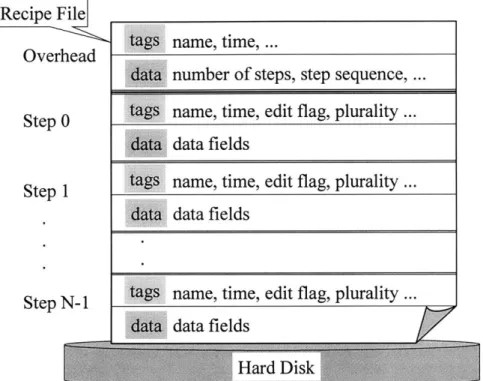
Figure 3.3 Structure of Recipe File 68
Figure 3.4 Object I/O Handling from Recipe Editor 69
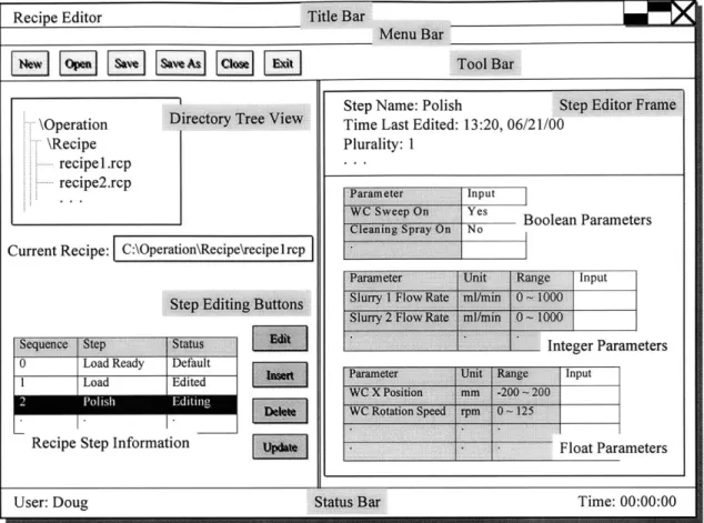
Figure 3.5 Recipe Editor User Interface 71
Figure 3.6 Wafer Carrier X Command Collision Avoidance Logic Sequence 75
Figure 3.7 Wafer Carrier Vacuum BitMap Handling 76
Figure 3.8 Error Handling of Manual Mode Overhead 77
Figure 3.9 Initialization Procedure of Manual Mode 77
Figure 3.10 Number Pad for Touch Screen 79
Figure 3.11 Manual Mode User Interface Screen 79
Figure 3.12 Sequential Functional Diagram of Load Method of Recipe Editor Link__ 84
Figure 3.13 Auto Mode User Interface 86
Figure 3.14 Sequential Functional Diagram of Sub-step MoveWCCA 92
Figure 3.15 Four Motion Stages of Sub-step MoveWCCA 93
Figure 3.16 Wafer Sweep Command Profile with Ramp Plus Sinusoid Input Shaper 97 Figure 3.17 Cyclic Position Command Generation Algorithm of sub-step SweepWC __ 97 Figure 3.18 Sequential Functional Diagram of Sub-Step BuffWafer 99
Figure 3.19 Sequential Functional Diagram of Step Polish 104 Figure 3.20 Design Parameter Tree of Process-level Control System 105
Figure 4.1 Schematic of Gantry X Axes Drive 107
Figure 4.2 Block Diagram Model of Each Gantry X Axis 110
Figure 4.3 Block Diagram of Synchronization Topologies Applied to Gantry Twin Axes
with Velocity Minor and Position Major Control Loop 111
Figure 4.4 Block Diagram of Adjustable Cross Compensation for Motion Synchronization
Applied to Gantry Twin Axes 112
Figure 4.5 Block Diagram of Gantry X Controller Implemented in Discrete Domain__ 118 Figure 4.6 Inputshaped Command and Each Axis Position Output of Gantry X Axes with
100 mm Step Command and 50 mm/sec Reference Velocity 119
Figure 4.7 Steady State Response of Gantry X Axes with 100 mm Step Command and 50
mm/sec Reference Velocity _ 119
Figure 4.8 Relative Error between Two Axes of Gantry with 100 mm Step Command and
50 mm/sec Reference Velocity 120
Figure 4.9 Inputshaped Command and Each Axis Position Output of Gantry X Axes with
200 mm Step Command and 100 mm/sec Reference Velocity 121
Figure 4.10 Exploded View of Command and Output Trajectory from Figure 4.9 (200 mm
Step Command and 100 mm/sec Reference Velocity) 121
Figure 4.11 Exploded View of Gantry X Position Trajectory from Figure 4.10 (200 mm
Step Command and 100 mm/sec Reference Velocity) 122
Figure 4.12 Relative Error between Two Axes of the Gantry with 200 mm Step Command
and 100 mm/sec Reference Velocity 122
Figure 5.1 Overview of CMP cc Machine Control System Interface 125
Figure 5.2 Schematic of Electrical Power Distribution of CMP cX Machine Control System 126 Figure 5.3 Schematic of Brushless DC Motor/Encoder/Amplifier Wiring 127
Figure 5.4 Photograph of Control Cabinet Assembled & Wired 129
Figure 5.5 Photograph of Switch Panel & ADwin 130
Figure 5.6 Photograph of Servo Amplifiers 130
Figure 5.7 Photograph of CMP cc Machine, oblique view 131
Figure 5.8 Photograph of CMP c Machine, front view 132
Figure 5.9 Semiauto Mode User Interface 132
Figure 5.10 StepPolish Editor and Number Pad 133
Figure 5.11 Photograph of CMP a Machine in Conditioning 135
Figure 5.12 Photograph of CMP a Machine in Polishing 135
List of Tables
Table 1.1 National Technology Roadmap for Semiconductors 11
Table 1.2 2002 CMP Production Tool Performance Targets 15
Table 2.1 Mission Statement (Highest Level FR) 22
Table 2.2 Decomposition of Mission Statement 23
Table 2.3 Decomposition of Machine-level Control System 24
Table 2.4 Decomposition of I/O Unit 26
Table 2.5 Decomposition of Machine I/O Unit 26
Table 2.6 Decomposition of Process-level I/O Unit 30
Table 2.7 Decomposition of Signal Processing Unit 31
Table 2.8 Decomposition of Controller Unit 37
Table 2.9 Decomposition of On-off Controller 37
Table 2.10 Decomposition of On-off Controller Structure 39
Table 2.11 Decomposition of Open-loop Controller 41
Table 2.12 Decomposition of Open-loop Controller Structure 42
Table 2.13 Decomposition of Closed-loop Controller 43
Table 2.14 Decomposition of Closed-loop Controller Structure 47
Table 2.15 Decomposition of Machine-level Overhead 50
Table 2.16 Decomposition of Software Structure 53
Table 2.17 Decomposition of Software Initialization 54
Table 2.18 Decomposition of Event Sequence 55
Table 2.19 Decomposition of Software Termination 59
Table 3.1 Decomposition of Process-level Control System 61
Table 3.2 Decomposition of Supportive Unit 62
Table 3.3 Decomposition of Recipe Builder 63
Table 3.4 Decomposition of Recipe Classes 65
Table 3.5 Decomposition of Recipe File 67
Table 3.6 Decomposition of Recipe Editor 69
Table 3.7 Decomposition of Editor User Interface 70
Table 3.8 Decomposition of Process Unit 72
Table 3.9 Decomposition of Manual Mode 73
Table 3.10 Decomposition of Manual Mode Overhead 74
Table 3.11 Decomposition of User Interface 78
Table 3.12 Decomposition of Machine-level Interface 80
Table 3.13 Decomposition of Auto Mode 81
Table 3.14 Decomposition of Auto Mode Overhead 82
Table 3.15 Decomposition of Recipe Editor Link 83
Table 3.16 Decomposition of User Interface 85
Table 3.17 Decomposition of Machine-level Interface 87
Table 3.18 Decomposition of Process steps 88
Table 3.19 Decomposition of Sub-steps 89
Table 3.20 Decomposition of Transport Sub-steps 90
Table 3.21 Decomposition of Sub-step Move_WCCA 90
Table 3.22 Decomposition of Sequential Algorithm 91
Table 3.23 Decomposition of Wafer Polishing Sub-steps 94
Table 3.25 Decomposition of Sub-Step BuffWafer 98 Table 3.26 Decomposition of Conditioning Sub-steps 100
Table 3.27 Decomposition of Step Polish 100
Table 3.28 Decomposition of Sequential Algorithm (StepPolish) 101 Table 4.1 Numerical Values of Gantry X Control System Constants (for each axis) ___ 110 Table 4.2 Numerical Values of Position Servo Controllers 123
Chapter 1. Introduction
1. Machine Control System Design
The scope of a machine control system design is quite extensive. It includes the selection and configuration of major system components, such as computers, controllers,
motors, amplifiers, etc., the wiring of those components to establish signal interfaces, the design of open-loop and closed-loop controllers, organizing and programming individual controllers to form a whole scale machine control system, providing an easy-to-use interface to machine operators, and so on. People often identify designing servo controllers with designing a whole machine control system; a user interface shown on the host computer screen with its control system. But they are just parts of a control system. The design and development of a control system involves more than simply designing its subcomponents (although quite important).
A machine control system can be conceived as a set of constituents or subsystems (both hardware and software) with its overhead structure, intended to drive individual components of the machine in a well coordinated manner to achieve the desired changes on target objects with a reduced or minimum human intervention. At a low level, a control system may be used to place a work piece precisely, instead of a human operator performing positioning task. At a higher level, the same control system may cut a complicated three dimensional shape out of the work piece based on a CAD drawing, automatically without a human intervention during the whole process of cutting.
The development (design and subsequent implementation) of a machine control system requires a sound knowledge of physical hardware, control technology, software engineering and system integration, due to the scope involved. In addition, a systematic design tool is required to structure the whole system and to guide the design of its components. Although there are some methodologies in specific disciplines, such as object-oriented programming in software engineering, no comprehensive tool seems to exist tobe able to encompass all the realms involved. Naturally, the development of various control systems has relied on human experience and trial-and-error, without any universal framework. As a result, one control system developed for a certain type of machine can not be used for a different type of machine. At each occasion, the time and cost of a machine control system development is substantially high due to the lack of interchangeability and reusability, the product of an ad hoc development. Also a system developed without any discipline often contains fatal errors undetected during its design phase, resulting in the endless upgrade and maintenance cycle, sometimes harming the very profitability of the system.
The control system design based on Axiomatic Design (AD) is proposed in this thesis. AD provides a concrete scientific methodology for the system development, by
identifying Customer Attributes (CAs) first, setting up independent Functional Requirements (FRs), conceiving appropriate Design Parameters
(DPs),
and also selecting Process Variables (PVs). Instead of relying on speculations and trial-and-errors, AD ensures a coherent new system development by clearly stating FRs and choosing right DPs, and by showing their relationships in terms of design equations. The Axiomatic Design approach eliminates unnecessary couplings and promotes innovative ideas throughout the entire design process. For a more detailed description about Axiomatic Design, please refer to Suh[3, 4].As an example, the control system for the CMP a machine will be designed and implemented throughout this thesis, based on the Axiomatic Design approach. The machine is a prototype semiconductor wafer processing machine developed at MIT. The detailed explanations about the background of the machine are to be presented in the following sections.
Table 1.1 National Technology Roadmap for Semiconductors
* DRAM: Dynamic Random Access Memory ** ASIC: Application Specific Integrated Circuits *** CD: Critical Dimension
**** ILD: InterLayer Dielectric
Year of First Product 1997 1999 2001 2003 2006 2009 2012 Shipment- DRAM*
Minimum feature size 250 180 150 130 100 70 50
(pim) I _t_4 I Bits/chip- DRAM 64M 256M 1G 1G 4G 16G 64G Chip size (mm2) - DRAM 280 400 445 560 790 1120 1580 -Logic 300 340 385 430 520 620 750 - ASIC** 480 800 850 900 1000 1100 1300 Maximum Substrate 200 300 300 300 300 450 450 Diameter (mm) Number of metal levels
- DRAM 2-3 3 3 3 3-4 4 4
- Logic 6 6-7 7 7 7-8 8-9 9
Maximum interconnect 820 1480 2160 2840 5140 10000 24000 length- logic (meter/chip)
Planarity requirement 300 250 230 200 175 175 175
within litho field for minimum interconnect
CD*** (nm)
Minimum metal CD (nm) 250 180 150 130 100 70 50
Metal height/width aspect 1.8 1.8 2.0 2.1 2.4 2.7 3.0
ratio- logic
Minimum contacted/non-contacted pitch (nm)
- DRAM 550/500 400/360 330/300 280/260 220/200 160/140 110/100 - Logic 640/590 460/420 400/360 340/300 260/240 190/170 140/130 Metal effective resistivity 3.3 2.2 2.2 2.2 2.2 < 1.8 < 1.8
(pQ-cm)
Barrier/cladding thickness 100 23 20 16 11 8 6
(nm)
ILD**** dielectric constant 3.0-4.1 2.5-3.0 2.0-2.5 1.5-2.0 1.5-2.0 1.5 1.5
(K)
2. Chemical-Mechanical Planarization (CMP)
Since the advent of Integrated Circuit (IC) technology, microelectronic devices have been fabricated on tiny pieces of semiconductor material, or on chips. A microelectronic chip is composed of numerous circuit components, or devices, such as transistors, diodes, resistors, and capacitors. Several layers of dielectric and metal materials are grown or deposited on top of the base silicon wafer, and these circuit features are created by a variety of methods such as diffusion, oxidation, lithographic patterning, etching, etc. A single wafer usually contains tens of 'dies', which are electronically complete units. Each die is sliced from the wafer, and then bonded and packaged to provide electrical connections and a more
rugged support.
Each device is composed of many features, such as a metal line, a segment of doped silicone substrate and a portion of dielectric layer. The topographic combination of these features produce transistors, diodes, resistors, capacitors, etc. These devices then constitute a microelectronic chip. Feature sizes are getting smaller with the advance of integration. A typical feature size is less than a micron, while 0.15 ptnm is becoming the current generation.
Table 1.1 is the National Technology Roadmap for Semiconductors, which shows the trends and requirements in the semiconductor industry for the next decade[1].
To meet the stringent requirements of submicron feature size, the layers deposited or grown during fabrication processes must be flat. The thickness variation of a layer over a device scale should understandably be much smaller than its feature size. Without this level of planarity, many fabrication techniques, especially lithography, fail to produce the desired submicron features. Before Planarization E oxide After Planarization I... U ml I U U m mi E substrate
Figure 1.1 Schematic of Microelectronic Features before and after Planarization
ILD Planarization
Metal Damascene
F
wafer
wafer carrier - abrasive slurry pad
i
platenC 3CO p
F: normal force
cow: wafer angular speed
(oP: platen angular speed
Rotary kinematics
wafer
wafer carrier abrasive slurry
platenfluid bearing belt/pad
-I-F: normal force oW: wafer angular speed v: belt speed
Belt kinematics
Figure 1.2 Two Types of Polishing Kinematics
Metal layers are planarized to expose the underlying microelectronic circuitry, whereas oxides are planarized to provide flat base layers for further depositions or growths of upper layers in the subsequent processes. Types of metals to be planarized include copper (Cu, dual damascene), tungsten (W, vias planarization) and aluminum (Al, alternative to Al etching). Figure 1.1 shows the schematic of the microelectronic features before and after planarization for both metal and oxide.
Planarization is usually accomplished by polishing a wafer mechanically against a pad in the presence of slurry, which is a mixture of loose abrasives and chemicals suspended in
water. For this reason, CMP is also interpreted as Chemical-Mechanical Polishing. A polishing process requires pressure and relative displacement between the two bodies in contact. Pressure is usually created by pneumatically pressing the wafer in a container (wafer carrier) against the pad on top of the platen. Relative displacements can be generated either by rotating the pad with the platen (rotary kinematics), or by the pad only with a stationary platen (linear or belt kinematics). In either case, the wafer is also rotated to ensure uniform polishing profile across the wafer surface and also to increase the relative speed seen from the wafer surface. Figure 1.2 shows the two types of polishing mechanism schematically.
3. CMP Performance Requirement
A CMP equipment should be able to process wafers to the desired specifications (effectiveness) in an efficient manner, as in any manufacturing machine. CMP specifications include uniformity, surface quality, defect density, etc. Throughput rate, cost of ownership, and tool capital cost can be the measures of a tool efficiency.
Uniformity can be classified into three levels- wafer, die, and feature level. On wafer level, non-uniformity (or variation in uniformity) is usually quantified by the standard deviation of a layer thickness divided by the mean thickness of the layer (&-/h). The lower is the thickness variation, the lower is the non-uniformity, meaning more planar surface. From the production point of view, wafer-to-wafer uniformity as well as within-wafer non-uniformity is important.
On die level, a difference in pattern (or feature) density leads to a difference in polishing rate and thus creates a non-uniformity. In metal polishing, the metal in high density area (i.e. which has more metal lines compared to the surrounding area) gets polished faster than the one in low density area, leading to overpolishing the underlying oxide layer. One solution to this problem is to use a selective slurry- the chemical in the slurry has a preferable etch rate to metal compared to oxide, thus minimizing oxide overpolishing.
On feature level, the cross section of an interconnect metal line tends to develop a hollow indentation after polishing, termed 'dishing.' Metal lines typically lose 20 % of their designed volume by the combination of dishing and overpolishing. A slight overpolishing is desirable to prevent any possible short circuit between the metal lines due to the metal residue over them.
Surface quality is closely related to defects. The polishing action can generate scratches comparable to the abrasive size used. The industry widely uses 50 to 300 nm size abrasives, which is close to the underlying feature size of the wafer surface. A streak of scratch can ruin many devices, considering it can be millimeters or centimeters long. The scratches should be minimized to the possible extent. Also the surface roughness should be less than 10 nm (R).
Mechanical abrasion and chemical etching during polishing can damage underlying features. Scratches are commonly observed. Weakly laid features can also be damaged by the contact with the abrasive particle, resulting in defects. A defect can also be created by an
impurity particle embedded during polishing or attached after polishing. Buffing (polishing with light pressure and only with water after main polishing) and post-CMP cleaning are
essential to remove any impurity from the wafer surface.
Porous polyurethane is typically used as a pad material in the conventional loose abrasive polishing, because of its chemical stability, low cost, and ease in tuning the
mechanical and physical properties. However as polishing continues, the surface of a pad plastically changes by the rubbing and plowing actions of abrasive particles. Pores are filled and the surface hardness changes (pad surface is glazed). These deformations result in the decrease in the material removal rate (MRR) and in the deterioration in the wafer uniformity and surface quality. To minimize this effect, the pad surface is continually regenerated during and/or between polishing by rubbing the pad surface with a fixed abrasive disk. This refreshing process is termed 'conditioning' in CMP industry. Diamond grits are typically used as the conditioning abrasives. Conditioning maintains a certain degree of pad roughness and keeps a number of pores open.
Table 1.2 2002 CMP Production Tool Performance Targets
Attribute Metrics for Dielectrics Metrics for Metals
Equipment Auto pad condition Required Required
Parameters In-line metrology Desired N/A
End point detector for STI Required N/A
application
In-situ thickness monitor and N/A Desirable control or endpoint control
Integrated with post-CMP clean N/A Required
Dry in-Dry out Required Required
Process CMP uniformity total variability 10% 10%
Targets (3a)
Head to head variation (3a) 1% 1%
Defects On-film @ 0.20 ptm <12.8/wafer (0.0186/cm2) <12.8/wafer (0.0186/cm2) (with in-situ On bare Si @ 0.09 jim <64.3/wafer (0.0919/cm2) <64.3/wafer (0.0919/cm2)
CMP Backside on Si @ 0.20 pm <200/wafer (0.30/cm2) <200/wafer (0.30/cm2) integrated
post-clean)
Cost/Perform Throughput 75 wafers/hr 75 wafers/hr
Targets Tool capital cost $1.9M $1.9M
Mean Time Between 300 hrs 220 hrs
Failure(MTBF)
Mean Time To Repair(MTTR) 2 hrs 2 hrs Preventive maintenance 6 hrs/wk 6 hrs/wk
Consumables <$4/wafer pass <$4/wafer pass
Area per tool 7.9 m2 7.9 m2
Support area per tool 2.8 m2
2.8 m2
CoO Target CoO objective $5.56/wafer pass $5.57/wafer pass
In the semiconductor industry, metrology is of the utmost importance. Metrology is required in almost all the process controls, yet measurements at nanometer level are quite challenging. A wafer can be measured during (in-situ) or at the end (ex-situ) of a process to check if the required physical changes have occurred. In-situ measurement is usually preferred, because the measured information can be fed to the controller for real-time process control purposes. But in-situ measurement is usually more difficult and costs more than ex-situ. Ex-situ measurement is applied where in-situ is not viable. Each wafer and/or die is tested and if it doesn't meet the process requirement, it is either sent back for re-work or discarded. Minimizing the amount of re-work and scrap is a big aim in the industry.
In CMP, the in-situ measurement is still not well established. The end of polishing (endpoint) is indicated by the amount of polishing time, which is set beforehand based on
the experiments and trial-and-error. To reduce the amount of rework, the wafers are usually overpolished slightly. It becomes essential to have an in-situ measurement capability to signal the endpoint at a right moment. Several methodologies are being used or under investigation: motor current sensing (friction force), film thickness measurement (acoustic, optical, electrical), etc.
Material removal rate (MRR) is of great concern, because it plays a major part in determining the throughput rate of a CMP tool. Thus a higher MRR is desirable. But increasing MRR beyond a certain point can reduce uniformity and surface quality. An optimum MRR increases the efficiency of the equipment, yet ensuring the effectiveness of the process it provides.
Throughput rate is not only affected by MRR, but also affected by other factors such as wafer handling and transportation time, cleaning time, conditioning time (ex-situ), number of heads and platens in a single machine, scheduling of individual process, etc. Throughput rate is a system issue indeed, and the request for a specific rate is to be met by considering those factors altogether.
There also are other measures of tool efficiency: tool capital cost, consumable cost, cost of ownership, tool size, ease of maintenance, etc. Table 1.2 shows the 2002 Production Tool Performance Targets from Semiconductor International magazine[2].
4. CMP a Machine
In order to meet the growing research need, a CMP machine has been developed at MIT by the CMP research group, as a successor of the simple test-bed machine developed two years ago. This cc machine has a great flexibility and a high precision, and designed to excel other commercially available machines. Figure 1.3 shows the drawing of the machine. The machine has one wafer carrier head and two platens, which enable multi-step polishing. The wafer carrier is mounted on the bracket, and the bracket can move up and down along the gantry Z axis. The gantry also provides X directional wafer carrier transportation. Two synchronized motors on each side of the gantry transmits x directional motion to the gantry via ball screws. The wafer carrier and the platens have their motors for rotation. The conditioner has one motor for the rotation of its head and also the other motor for the X direction transportation. Loading, unloading, and cleaning of a wafer are all performed at the load/unload/cleaning station. All of these components are mounted on top of the granite table, which has a good vibrational damping characteristic. The table is then mounted on the steel supporting structure.
There are several distinctive features in the machine. The machine is designed with precision in mind. Flatness of the granite table and the platens are ensured. Verticality of the gantry Z axis, the wafer carrier spindle, and the platen spindles are also double checked. All the translational motions will be controlled with less than 50 pm of precision, and all the rotational motions will have error bounds of ±0.1 rad/sec. The machine can provide wider range of process parameters. It can achieve 4 m/s of relative polishing speed, whereas other tools are typically limited to 1 or 2 m/s. It also provides polishing pressure of up to 20 psi,. However nominal polishing pressure is usually 7 psi.
Depending on the CMP process development, the machine may be asked to perform multi-step polishing. A wafer can be polished for a given amount of time on one platen with a certain set of process parameters- pressure, velocity, abrasive size and material, slurry
chemical, pad material and physical property, etc. Then it will be transferred to the other platen with a different set of process parameters. Usually a platen is dedicated to a specific slurry and pad, but other process parameters can be changed even within a single platen. A plausible scenario is two-step metal polishing: First step for major material removal with high speed and pressure, and large abrasive size; Second step for finishing and planarization with low speed and pressure, fine abrasive size, and selective chemicals. The machine is mainly designed for metal (Cu) polishing, but can also be used for oxide polishing and even for polymeric ILD polishing.
Gantry Wafer Carrier Load/Unload/Cleaning Station Conditioner Platen - Granite Table C) S Sport Structure z
Figure 1.3 Overview of CMP cc Machine
Two
different
types of slurry canbe delivered
to each platen at the same time. The slurrydispense
lines canbe
usedfor deionized
(D1
waterflushing.
A slurry canbe dispensed
either on top of the platen, or through the platen
for
abetter
slurry transportation. When a slurry is dispensed only on the top of the platen, it is often difficult for the slurry to flow to the middle of the polishing interface. The edge sees more slurry then the center, and thus it usually gets polished faster, contributing to the non-uniformity. By dispensing slurry through the holes in the platen and pad, an even distribution of slurry is achieved.An optical sensor is embedded in the platen, which measures intensity of the reflected light, or reflectance, from the opposing surface, which is the wafer being polished. Metal has higher reflectance than oxides. Thus at the end of metal polishing, once underlying oxide layers are exposed, the reflectance value will drop significantly. By employing this principle, the reflectance measurement can be used for endpoint detection in metal
polishing. Signal acquisition methods and signal processing algorithms are being developed for Cu endpoint detection.
Many factors can affect the uniformity of the wafer surface- uneven pad profile, uneven slurry distribution, spatial difference of relative velocity over the polishing interface, etc. Due to the rotation of wafer, the circumferential layer thickness variation is usually less than the radial one. Typically, edge is being polished faster than the center, leading to a convex profile. In part to combat the problem, the pressure actuation compartment of the wafer carrier is divided into four concentric chambers, called Active Membrane Assembly (AMA), which can have different pressures. For example, to prevent the convex profile, the inner compartments may exert higher pressures, where as the outer compartments lower pressures. Another possibility is to actuate membranes dynamically from the reflectance feedback. Reflectance measurement can give the information about the remaining metal layer thickness (or if it is completely removed). The machine control system keeps track of the sensing position on the wafer. By combining film thickness metrology and spatial information, it is possible to actively actuate AMA during polishing. For example, if an area corresponding to the third compartment is detected to be polished faster than the rest, the process controller tells the AMA to reduce the pressure in the third compartment.
5. CMP a Machine Control System Overview
The machine control system needs to be designed to ensure the effectiveness of the CMP process and enhance the efficiency of the machine operation, by integrating all the intended system functions. The control system development includes the electrical wiring and interfacing of various actuators, sensors and the controller; the design and implementation of individual control algorithms (or controllers) for each drive and actuation component; creation of process steps, such as wafer loading, buffing, conditioning and polishing, which are generated by time-wise and conditional combinations of individual control actions; realization of machine operation, which allows a user to process sets of wafers to the desired specifications, using the various process parameters and sequences (recipe) in a fully automated environment.
The control system has a cabinet which houses most of the electrical components separate from the machine. The external processing system (a computer for system control) is located inside the cabinet. A 19" rack mountable, modular system, called ADwin, is selected as the real time process controller. ADwin has its own local 40 MHz RISC (Reduced Instruction Set Computer) DSP (Digital Signal Processor) and 32 MB of memory. Analog-to-Digital (AD), Digital-to-Analog (DA), Digital-In-Out (DIO), counter, relay modules can be mounted on the ADwin controller. The processor communicates with these modules via ADwin bus. For more information about ADwin, refer to its manual[12].
A host computer is required for the initial loading of the control program to ADwin and the communication and supervision while the controller is at work. A personal computer (PC) is selected for this purpose. The PC has a graphical user interface (GUI) to interact with a user, to save and edit recipes, and to monitor the machine operation. The PC has a Pentium III, 450 MHz CPU and runs under Windows NT 4.0 environment. It has a flat panel LCD (liquid crystal display) touch screen for an easy user interaction. Figure 1.4 gives the general idea of the CMP a machine control system.
GUI Communication
User <TC>C Fab Environment
Control Board
on Pressure Flow Temperature Sensin
rol Unit Control Unit Control Unit Control Unit
tr PneumaticS
iton Actuator+
;iio DI Water TMachine a
tation LOConditioner Slur
Moti Cont Poa Ro IArn~ ten tation
Figure 1.4 Overview of CMP (x machine Control System
The machine has nine motors, with nine corresponding switching amplifiers. They all have incremental rotary encoders for position feedback. Two pumps are used to deliver slurries and DI water for each platen. Numerous valves are required for slurry and DI water transport control and for pneumatic control. Endpoint and wafer detection sensors are used for process control purposes. In addition, there are numerous relays for on/off type actuation. All these devices are located either in the control cabinet or on the machine and wired both in power and logic.
Wiring requires a careful planning and cautious implementation, because a single misplaced wire can ruin the whole control system. Wiring is also a greatly time consuming process. The biggest concern in wiring is to minimize noise pickup, generated from switching amplifiers and other electronic devices. Noise can interfere with the signal in/out
(I/O)
processing of the ADwin and the communication between the host PC and the ADwin. A small glitch can stop the whole machine and also undermine the safety of the machine operation. Certain methods will be employed to suppress the noise from propagation. But usually, they can not eliminate noise completely. The issue here is how to keep the noise below a certain level, so that the control system can perform its normal functions without being affected by the noise.Once wiring is completed and proper signal I/Os for the ADwin are established, the next task is to design digital controllers. Digital controllers are implemented as software programs which run on the ADwin controller. Although confusing, the term controller is
Un7it]
ct
ry unt
used to mean both an external control circuit board (such as ADwin) and a specific control algorithm for a drive.
Relays and On/Off controls require just a single line of coding in control software. All the pneumatic and fluid valves will be controlled in open-loop, but they need to be calibrated so that the dictated value from the controller matches with the actual physical value in the valves. Analog sensors, such as the reflectance sensor and the strain gages need calibration, too.
For the CMP a machine, all the position and velocity components will be controlled in closed-loop. The gantry X axis, the gantry Z axis, the conditioner X axis and the wafer aligner angle are position controlled. Synchronization of two axes motors and providing fast enough speed for the heavy gantry mass (approx. 1100 Kg) are challenges of the gantry X axis position controller development. The weight of the wafer carrier (approx. 300 Kg) and maintaining the vertical position are the concerns in the gantry Z axis controller design. Conditioner X position control is expected to be relatively easy because of its light dynamics. But coordinating its motion to avoid any collision with the wafer carrier is a demanding subject. Four arm wafer aligner is located in Loading/Unloading/Cleaning Station (LUCS), to center the wafer before the wafer pickup by the wafer carrier. A proper force control is required in order not to crush the wafer during aligning.
Velocity control is relatively easier than position control. The wafer carrier rotation, the two platen rotations and the conditioner rotation are all velocity controlled. The issue here will be maintaining a set velocity under the load, such as polishing or conditioning. Having functional individual controllers at hand doesn't necessarily mean we can polish wafers. We have to create an intelligent set of the control actions, generated by the designed controllers, to embark any processing. For example, to move the wafer carrier from a position (X1, Z1) to (X2, Z2), we have to call both X and Z controllers with a certain sequence and possibly multiple times.
A small set of control actions can be designated as a 'sub-step.' A sub-step refers to a set of individual control actions, which is identifiable as a single unity during wafer processing. Wafer transport, wafer sweeping during polishing and wafer buffing can be the examples of the sub-step.
These sub-steps and other procedures can be combined to form a 'step,' which is a distinctive set of processes in the continuous stream of wafer processing. A step is an ingredient to form a recipe. By combining various steps, a process recipe can be designed. Loading, unloading, polishing and cleaning can be the examples of the step. The grouping is rather arbitrary, but performed in the viewpoint of a user, who has to design a recipe to obtain the desired product. Recipe is a set of process parameters and sequences to induce the desired physical change to a wafer which has a certain film layer (material, thickness, topography, etc.) to be planarized with underlying features.
The process control software will be designed to accommodate various possible recipes to run the machine. The process control software will send process commands to the machine control software. The machine side will recognize the commands from the process side, collect process data, perform required control actions, and update process parameters and machine status to the process side.
On the PC side, it will have a GUI, where the user can edit and retrieve recipes and operate the machine. Machine operation involves loading and unloading of control program to ADwin, loading and unloading of recipes, sending function commands (Run, Stop, etc.), supervising the work of ADwin control software, receiving process parameters and machine
status data from ADwin and updating on the GUI operation screen. Supportive features, such as set up, machine operation database (machine use log), and maintenance log should be included on the PC side.
6. Thesis Objective
The objective of this thesis is to develop the CMP cc machine control system successfully, using the framework of Axiomatic Design. During the course, it will become evident that Axiomatic Design can provide a systematic design methodology for a complex control system design. Main hypotheses include:
1. Axiomatic Design can provide a systematic framework and guideline in developing a complex machine control system.
2. Axiomatic Design clearly identifies required control actions (FRs), corresponding controllers (DPs), and run-time control variables (PVs).
3. Modern control technology can be employed to realize the control action specified by AD during the decomposition with a reasonable tolerance (Controller design follows Axiomatic decomposition).
4. Axiomatic Design can be used to design the structure and the sequence of the process control software.
5. Hierarchical structuring and abstraction between the levels in a software improves readability, efficiency, and maintainability of the system, which are the natural consequence of software design based on Axiomatic Design.
6. The structure designed by AD is realizable by the current software technology (Programming follows Axiomatic decomposition).
7. Thesis Overview
This chapter has been the introduction, outlining the work involved in the CMP cc machine control system development and presenting the objective of this thesis. In Chapter 2, the machine side control system is developed using the AD framework. The development continues in Chapter 3, which presents the design of the process control system. Chapter 4 deals with the design of a servo controller and its implementation. The entire system is integrated and implemented in Chapter 5. The conclusion is given in Chapter 6. The discussion about the future work follows in Chapter 7.
- -- El- ~
-Chapter 2. Machine-level Control System
Axiomatic Design begins with identifying customer needs(Customer Attributes, CAs). In the case of the CMP cc machine control system development, customers include MIT CMP research group(both the design and the process team), the research sponsor, and potentially the semiconductor industry as a market. Many of the needs have already been remarked in the introduction chapter. The following lists the most fundamental CAs.
* Provide the required precision. * Minimize the non-processing time.
" Enable a fully automated wafer processing. " Flexible recipe editing and its implementation.
* Provide an equipment use and maintenance log. * Easy to operate.
* Safe to use.
These CAs can also be thought of as general guidelines or constraints throughout the overall system development process. These constraints will be explained more elaborately at each corresponding level.
Axiomatic decomposition often starts with a single objective or mission statement. In this case, the objective is clear: Integrate individual components to create an effective and efficient machine control system. Table 2.1 shows the mission statement, which serves as the highest level FR/DP set.
Table 2.1 Mission Statement (Highest Level FR)
Coordinate the individual components of the CMP cx Equipment control system machine in a systematic manner so that it can process wafers
effectively and efficiently to the desired specifications.
In the CMP a machine control system development, the issues are three fold: hardware interfacing, generating individual control actions, organizing those control actions to process wafers. Hardware interfacing belongs mostly to the domain of Electrical Engineering, employing the knowledge of circuit design, power electronics, signal conditioning, etc. Design of an individual controller also belongs to the realm of Control Engineering, with the indexes of tracking error, response time, robustness, optimization, etc. However, providing a framework for individual controllers and organizing the output of the controllers to achieve higher level goals are mostly system design issues. Thus, AD can be used from the beginning to structure the control system. AD can not design a controller itself. A controller is designed from the principles of Control Engineering. But it will identify
the need of a certain type of controller to achieve FRs and place the controller as a DP, through the decomposition. Also, AD will be used to identify and layout the elements and methods of a controller, because a digital controller is essentially a block of coding running
We define the equipment control system as a set of software designed to achieved the goal of coordinated wafer processing, with appropriate interfaces to the machine and the user. Thus it is natural to decompose the highest level FR into two sub FRs: Machine-level
and Process-level. Table 2.2 is the decomposition of the mission statement. Table 2.2 Decomposition of Mission Statement
Contro Coordate otrociosfmec individual Machinn-levs coto sse mahe coPamponent. na yteai
Process Organize the controlled outputs for wafer Process-level control system processing.
FRI
X
o
DP1
FR2
XX_ DP2
Machine-level control system will concentrate on ensuring and structuring individual control actions of the machine, which are the basic ingredients of the overall equipment control system. Because it deals with the real time hardware control issues, it will be programmed for and running on ADwin external processing system. In contrast, Process-level control system deals with the issue of organizing these individual actions generated by the Machine-level to process wafers in desired manners. Thus it should supervise and communicate with the Machine-level, giving commands and taking statuses, interact with a user to accept user inputs and display machine parameters, and run the machine in a preprogrammed manner in an automatic wafer processing mode. Process-level control
software naturally nests on the host PC.
Although not specified in this decomposition, we can think of a third design parameter, DP3: Operation-level control system. Our present goal is to process a single wafer with a given set of conditions in a fully automated manner. But in a real production environment, we are interested in operating the machine to process lots of wafers. For example, we may want to process two lots of 50 Cu wafers with 0.13 ptm line width in the morning and a lot of 100 oxide wafers with 1 pm film thickness in the afternoon. Also, in a fab, a machine hardly works as a stand alone equipment. A CMP machine is usually located in a bay or cluster type configuration, with other equipments such as a cleaning station, an inspection station, and a wafer transporting and handling robot. Scheduling of the equipment, cooperation with other machines, and managerial supervision of 'operation' become important issues at this level. In most cases, this Operation-level control system will
run on a physically separate unit, such as a central processing and monitoring computer, connected via an intranet. DP3 addresses the necessity of a higher level control system and provides an interface for it. However, we will remain in the decomposition of DP1 and DP2, because the machine is more oriented to the research rather than the production.
It will simply be impossible to present every detail of the decomposition of all the branches and all the way down to the lowest levels. Rather, structuring of the system along the major branches will be described, with an occasional illustrative decomposition down to the required level where needs arise. We will first tackle the Machine-level control system. When we are comfortable with the clear picture of the Machine-level in mind, we will move on to the Process-level in the next chapter to zoom out.
DP1. Machine-level Control System
Machine-level control system is responsible for generating individual control actions of the machine in a systematic manner, so that they can be used as constituents in wafer processing and machine operation by higher level control systems. To meet the objective, a machine-level control system should have an In/Out(J/O) unit to handle communication with the machine and a higher level control system, an signal processing unit to condition incoming signals(mostly from the machine), a controller unit to command outputs to the machine and an overhead to structure and coordinate these units and the machine-level itself. Table 2.3 shows the decomposition of the Machine-level control system.
Table 2.3 Decomposition of Machine-level Control System
Control Receive inputs and send outputs. I/O unit
Control Process incoming signals. Si al processing unit Control Produce controlled outputs. Controller unit
4
Control Structure the Machine-level control system. Machine-level overheadFRl1
XOOO DPll
FR12
XXOO
DP12
FR13
XXXO
DP13
DP11. I/O Unit of the Machine-level Control System
The Machine-level control system basically interacts with the machine and the Process-level control system. In turn, the machine interacts with the environment and the Process-level interacts with a user and possibly an operation-level control system. Figure 2.1 conceptualizes the interactions of the Machine-level with other systems.
display logic & control commands machine parameter input performance
Process-level
Machine-level
Machine
t
t 4
user input status & control parameters controller output disturbance
* Logic commands: function buttons, initialization
* Control commands: position, velocity, pressure, flow rate, valve and switch on/off, etc. * Status parameters: error, operative status
* Control parameters: current position, velocity, sensor output, time, etc.
Figure 2.1 Interaction of Machine-level Control System with other systems We decompose the I/O unit into two sub units by their corresponding counter parts- the machine and the Process-level, as shown in Table 2.4. The machine I/O unit deals with the interface with the machine to acquire the data for machine control and transmit the output to drive the machine to the desired states. Thus the machine I/O works as a bridge between the machine hardware and the control system software. As one can imagine, the formation of the machine I/O depends largely on the hardware configuration. Types of actuators and sensors and the natures of their signal dictate the forms of the required interface cards. Basically inputs and outputs are either analog(continuous) or digital(discrete), and interface cards are built to handle varieties of those basic signals.
Table 2.5 shows the decomposition of the machine I/O unit. A counter(CNT) card is required to decode the position information from the encoder signals installed on the mating motor shaft. An encoder typically gives two channels of TTL(transistor-transistor logic) level square wave signal. As described in Figure 2.2, one channel leads the other depending on the direction of the rotation. The state transition sequence of a counter-clockwise(CCW) rotation is different from the one of a clockwise(CW) rotation. Thus by observing the state sequence, a counter can determine in which direction the shaft is
information by counting the transitions of states(quadruple decoding). Thus an 1000 pulses/rev encoder gives 4000 counts/rev resolution in quadruple decoding. Starting from 0, it will count 4000 if the shaft makes one CCW revolution, -4000 if one CW revolution.
Table 2.4 Decomposition of I/O Unit
Handle inputs from and outputs to the machine. Machine I/O unit Handle inputs from and outputs to the Process- Process-level I/O unit level control system.
{FR111 F X0 DP111
FR12f Lo X DP12
Table 2.5 Decomposition of Machine I/O Unit
Control I Acquire encoder(position) signal Counter(CNT) card Control Sense digital(Hi or Low) signal Digital Input(DI) card
Control Accept analog(continuous) signal Analog-to-Digital Conversion(ADC) card Control Send On/Off(Hi/Low) signal Digital Output(DO) card
Control Output relay signal Relay(REL) card
Control Provide analog output Digital-to-Analog Conversion(DAC) card
FRI I
FRI 112
FR1113
FR1114
FRI115
FRI116
x 0 0 0 0 0
0 X 0 0 0 0
O X O O
0
0 0 0 X 0 0
O OO
O X O
O O O 0 X
DP1111
DPI 112
DPI
113
DP1 114
DPI
115
DP1
116
CCW: A leads B
A
90 elec. deg. 1 cycle time CW: B leads A A ___ B5 V Channel A Channel B State
1 0 1
0 1 2
0 1 3
0 0 4
5 V Channel A Channel B State
1 1 2 0V 0 1 0 0 41 o 1i 2 CCW 4 3 2 CW 4 3
Figure 2.2 State Transitions of Two Channel Encoder
ADwin is equipped with 3 CNT-VR4 counter cards. Each CNT card has four counters with maximum input channel rate of 1.25 MHz(5 MHz quadruple count rate). Figure 2.3 shows the block diagram of a CNT-VR4 counter. Optionally each counter can be configured as a clock(single channel) and a direction(up or down) input. The output is stored as a 32 bit integer value in the register and transported to the CPU via ADwin-PRO bus.
clock dir
A
32 bit up/down counter quadruple(edge) -evaluation
- clear input
32 bit latch 'c ntrlu i
Internal ADwin-PRO Bus
Many on/off type sensors give TTL level signal, and a digital input(DI) card is required to capture the signal. Also a digital output(DO) card is required to transmit TTL level on/off signal either directly to an actuator or its amplifying circuit. ADwin has three Pro-DIO-32 cards with 32 digital input and output channels at TTL levels for each card. Each channel can be selected as input or output by software.
An analog-to-digital conversion(ADC) card is necessary to measure a continuous voltage signal. A Pro-Aln-8/16 card is equipped with a 16 bit ADC and 8 differential input channels, and has a maximum sampling rate of 50 kHz. ADC will be used to interface process sensors, such as a reflectance senor and strain gauges. Figure 2.4 shows the block diagram of the Pro-Ain-8/16 ADC card. Its output is a 16 bit integer variable for each channel.
1
Op >amp AD pt- data Hdata
ThePoE -6 rconverte d r register
2
pt- address addes
8 oude decoer
Figure 2.4 Block Diagram of Pro-Ain-8/16 ADC card
The Pro-REL-16 relay card has 16 isolated relay outputs. Each relay channel is driven to open or closed contact by the built in transistor switch, which is in turn controlled by a digital output. In that sense, it is a variation of DO card, with built in relays and transistor switches. Figure 2.5 shows a simple diagram of a relay output circuit. Each relay can switch up to 30 V AC/DC and 500 mA current.
Servo amplifiers and variable speed pumps usually accepts an analog voltage input as a command signal. In a computer controlled system, both open loop and closed loop controllers are implemented by a software program. Thus, to transmit a controller output to the corresponding plant, a digital-to-analog conversion(DAC) card is required. The Pro-Aout-8/16 has 8 channels of 16 bit DACs with fixed 1 order low-pass filters. Each channel can output up to ±10 V and 5 mA with 20 ptsec of settling time. Figure 2.6 shows the schematic of the Pro-Aout-8/16 analog output module.
relay outputs A Rel 00 ... 15 B +5 V DIG GND
Figure 2.5 Circuit Diagram of Pro-REL-16 Relay
Op low-pass DA
amp filter converter
2 Op low-pass DA
amnp filter converter
8 Op low-pass DA
amp filter converter
data data
register dat
address address register
Figure 2.6 Block Diagram of Analog Output Module, Pro-AOut-8/16
The Machine-level control system should also communicate with the Process-level control system to receive command inputs and provide machine status and process data. The ADwin system is equipped with two Analog Device's 40 MHz ADSP 21062 digital signal processor(DSP) chips. Each processor has two types of memory: 256 KB of internal memory to load program and local variables; 16 MB of external dynamic memory(DRAM) for array variables which are typically used for data measurement and storage. ADbasic, the programming language of ADwin, provides drivers so that a host PC can access the memories of the ADwin processors. For more information about the ADwin processor memory structure and accessibility, please refer to the ADbasic manual[5].
We use the memories of DSPs to design the Process-level I/O unit of the Machine-level control system. Table 2.6 shows the decomposition of DP112. Command inputs
-c 0
I
0
----r ~ - -~ -~ ~-=-~" - -~ - - -- ,-~
include both logic and control commands. Run, Stop, Reset, and Initialize are examples of logic commands, which mainly handles process controls. Control commands are instructions for desired control actions, such as position, velocity, and flow rate. The number of the command input is typically less than 100. Thus it is reasonable to use a section of the DSP internal memory writable by the host PC. By the same token, parameter outputs of the Machine-level control system are placed in a segment of the DSP internal memory, accessible by the host PC. Parameters include both status and control parameters. Status parameters indicate the status of the machine and the error code, if an error is set. Control parameters are machine parameters including, current positions, velocities, sensor values, time, etc.
A large amount of data(typically on the order of MB) is collected during wafer
processing for the purpose of measurement and on- and off-line analysis. Reflectance of wafer surface during polishing is an example of process data. If the host PC requires the data for a higher level analysis and storage, the ADwin should be able to temporarily house the data until the host come and pick them up. 16 MB of external memory of DSP can be used for this purpose. However, one should be careful not to overwrite the memory.
Table 2.6 Decomposition of Process-level I/O Unit
Receive command inputs
FRI
1211
X 0
DPI 121
FR1122
= xXO
DP1122
DP12. Signal Processing Unit of the Machine-level Control System
A raw signal from the machine first needs to be converted to an appropriate unit
used in the control system software, and then differentiated and integrated, if necessary. Typically, an incoming signal contains a lot of noise, superposed on the original signal. Proper filtering is quite essential in a high precision measurement and control. A controller output is also required to be converted to a required format by the I/O unit. Process date needs to be saved temporarily until requested by the Process-level control system.
Signal processing unit conditions incoming signals from the machine so that they can be used both by the Machine-level and the Process-level control system. Most signals are processed to be used by the Machine-level controllers, but some processed signals are fed directly to the Process-level for a higher level process monitoring and control. Wafer reflectance signal is an example of locally conditioned information, yet used for a higher level process control. Table 2.7 is the decomposition of the signal processing unit.
Table 2.7 Decomposition of Signal Processing Unit
Control Convert an input to the desired unit. Input conversion unit Control Differentiate an input signal. Differentiation unit Control Filter the input. Filtering unit Control Integrate required signals. Integration unit
Control Convert controller outputs to the I/O unit Output conversion unit
units
Control Save data internally. Internal data save unit
FR121
FR122 FR123FR124
FR125
FR126
X X X X X 000000
X 0 0 0 0 XX000 XXX00 XX XX0
0 0 0 O XDP121
DP122
DP123
DP124
DP125
DP126
An encoder counter gives a 32 bit integer value, but for control purposes it needs to be converted to an angle either in radian or degree. The following simple formula converts a count to a radian in an incremental manner. To decode an absolute rotary position( 0 ~