Publisher’s version / Version de l'éditeur:
Optics Letters, 36, 11, pp. 2110-2112, 2011-06-01
READ THESE TERMS AND CONDITIONS CAREFULLY BEFORE USING THIS WEBSITE. https://nrc-publications.canada.ca/eng/copyright
Vous avez des questions? Nous pouvons vous aider. Pour communiquer directement avec un auteur, consultez la
première page de la revue dans laquelle son article a été publié afin de trouver ses coordonnées. Si vous n’arrivez pas à les repérer, communiquez avec nous à [email protected].
Questions? Contact the NRC Publications Archive team at
[email protected]. If you wish to email the authors directly, please see the first page of the publication for their contact information.
NRC Publications Archive
Archives des publications du CNRC
This publication could be one of several versions: author’s original, accepted manuscript or the publisher’s version. / La version de cette publication peut être l’une des suivantes : la version prépublication de l’auteur, la version acceptée du manuscrit ou la version de l’éditeur.
For the publisher’s version, please access the DOI link below./ Pour consulter la version de l’éditeur, utilisez le lien DOI ci-dessous.
https://doi.org/10.1364/OL.36.002110
Access and use of this website and the material on it are subject to the Terms and Conditions set forth at
Temperature-independent silicon subwavelength grating waveguides
Schmid, J. H.; Ibrahim, M.; Cheben, P.; Lapointe, J.; Janz, S.; Bock, P. J.;
Densmore, A.; Lamontagne, B.; Ma, R.; Ye, W. N.; Xu, D.-X.
https://publications-cnrc.canada.ca/fra/droits
L’accès à ce site Web et l’utilisation de son contenu sont assujettis aux conditions présentées dans le site LISEZ CES CONDITIONS ATTENTIVEMENT AVANT D’UTILISER CE SITE WEB.
NRC Publications Record / Notice d'Archives des publications de CNRC:
https://nrc-publications.canada.ca/eng/view/object/?id=523844b8-a7f0-4172-b4f0-3047e0b5e01c https://publications-cnrc.canada.ca/fra/voir/objet/?id=523844b8-a7f0-4172-b4f0-3047e0b5e01c
Temperature-independent silicon
subwavelength grating waveguides
J. H. Schmid,1,* M. Ibrahim,2P. Cheben,1J. Lapointe,1S. Janz,1P. J. Bock,1A. Densmore,1
B. Lamontagne,1R. Ma,1W. N. Ye,2and D.-X. Xu1
1Institute for Microstructural Sciences, National Research Council Canada, Ottawa, Ontario K1A 0R6, Canada 2Department of Electronics, Carleton University, Ottawa, Ontario K1S 5B6, Canada
*Corresponding author: jens.schmid@nrc‐cnrc.gc.ca
Received April 4, 2011; accepted April 14, 2011; posted April 21, 2011 (Doc. ID 145382); published May 31, 2011
We demonstrate, by experiment and numerical calculations, temperature-independent subwavelength grating waveguides with a periodic composite core composed of alternating regions of silicon and SU-8 polymer. The poly-mer has a negative thermo-optic (TO) material coefficient that cancels the large positive TO effect of the silicon. Measurements and Bloch mode calculations were carried out over a range of silicon–polymer duty ratios. The lowest measured TO coefficient at a wavelength of 1550 nm is 1:8 × 10⁻⁶K−1; 2 orders of magnitude smaller than
a conventional silicon photonic wire waveguide. Calculations predict the possibility of complete cancellation of the silicon waveguide temperature dependence. © 2011 Optical Society of America
OCIS codes: 130.3120, 050.6624, 130.3130.
In recent years, much progress has been reported in the development of integrated silicon photonic devices and circuits, which are expected to have a major impact on optical interconnects and data transport applications. High index contrast silicon microphotonic waveguides are also used in emerging new applications in biosensing
[1] and spectroscopy [2]. An important issue with silicon
photonic circuits is the temperature dependence of their optical output signals, which is caused by the compara-tively high thermo-optic (TO) material coefficient of silicon (dnSi=dT¼ 1:8 × 10−
4
K−1). Precise external tem-perature control is, therefore, often required for silicon photonic devices, especially those incorporating inter-ferometers, resonators, and wavelength dispersive ele-ments. The temperature dependence of silicon wire waveguides can be reduced by using a polymer overclad-ding with a negative TO coefficient to compensate for the
silicon TO effect [3,4]. Athermal operation of
wave-guides, i.e., dneff=dT¼ 0, where neffis the mode effective index and T is the ambient temperature, is achieved if waveguide dimensions are chosen such that the relative overlap of the mode with the silicon core and the poly-mer cladding results in a cancellation of their respective contributions to the waveguide effective TO coefficient. This can be accomplished in narrow silicon wires with a
fairly delocalized mode [5], or with slot waveguides, in
which a large fraction of the modal field is confined to
a narrow gap filled with the low-index polymer [6].
Here we suggest a new principle for making athermal silicon waveguides, using the subwavelength grating (SWG) effect. We have recently demonstrated that silicon photonic wire waveguides with periodic gaps, of a period smaller than one-half of the effective operating wave-length, act as low-loss waveguides with a spatially
aver-aged core index [7]. A schematic illustration of a SWG
waveguide is shown in Fig. 1(a). In short, SWG
wave-guides operate in the long wavelength regime of the dis-persion diagram, well below the frequency of the first stop band. Their fundamental mode is a bound Bloch mode, which is, in principle, lossless. Since the period of the grating etched into the waveguide is well below
the operating wavelength, its fine structure is not re-solved by the light and diffraction is suppressed. There-fore, the optical properties of the SWG waveguide resemble those of a channel waveguide with a spatially averaged core index. Spatial index averaging offers the opportunity of mitigating the silicon TO effect by filling the gaps with polymer material of negative TO coefficient for an appropriate grating duty ratio. The polymer used in
our work is SU-8, which has a refractive index of nSU-8∼
1:58 at λ¼ 1:55 μm and a TO coefficient of dnSU-8=dT¼
−1:1 × 10− 4
K−1 [8].
In Figs. 1(b)–1(d), we show scanning electron
micro-scope images of three fabricated SWG waveguides of
470nm width, 250 nm grating pitch, and duty cycles of
(b) 46%, (c) 56%, and (d) 66%. These waveguides were fabricated from commercial silicon-on-insulator sub-strates with 0:26 μm thick silicon and 2 μm thick buried oxide layers. We used electron beam lithography to de-fine the waveguides and transferred the pattern into the silicon layer by inductively coupled plasma reactive ion
etching using a mixture of SF6 and C4F8gases. The
sam-ples were coated with a 2-μm-thick SU-8 polymer layer by a standard spin and bake procedure. To measure the TO coefficient of the composite silicon–polymer SWG wave-guides, the structures were incorporated in unbalanced Mach–Zehnder interferometer (MZI) devices, as shown
in Fig.1(d). Standard photonic wire waveguides are used
for the Y splitters, and the waveguide bends while each arm of the MZI includes two straight SWG sections. Wire waveguides are adiabatically transformed to SWG
wave-guides at the positions indicated by arrows in Fig.1(e),
with coupler structures similar to the one described in
[9]. The combination of wire and SWG waveguides in
the same device demonstrates the compatibility of the two waveguide types. SWG waveguide propagation loss has previously been found to be of comparable
magni-tude to our photonic wires [7]. The two arms of the
MZI are identical except for the additional SWG
section length of ΔL ¼ 3 mm inserted into the upper
arm. The transmitted intensity of the MZI interfero-meters will, therefore, have the usual sinusoidal form
2110 OPTICS LETTERS / Vol. 36, No. 11 / June 1, 2011
I¼ cos2
ðk0=2 neff ΔLÞ, where neff is the effective index of the silicon–polymer composite SWG section.
Figure2shows the results for optical transmission of
MZI devices with SWG waveguides of varying duty cycles at different temperatures. For these measurements, the chips were mounted on a temperature-controlled copper heat sink. For waveguides with a duty cycle of 100%,
i.e., conventional photonic wire waveguides, a positive wavelength shift of approximately 70 pm=°C is observed [Fig.2(a)]. In comparison, the sign of the shift is reversed and the magnitude reduced for SWG waveguides with a
duty cycle of 46%, as seen in Fig. 2(b). For the SWG
waveguides with a duty cycle of 66% in Fig.2(c), the
tem-perature-dependent shift of the transmission spectrum is minimal, indicating nearly athermal waveguide behavior.
All spectra shown in Fig.2are for quasi-TE polarization.
For our configuration of the MZI device, the waveguide
TO coefficient dneff=dT can be derived from the
wave-length shift dλ=dT of the transmission spectra: dneff dT ¼ ng λ dλ dT; ð1Þ
where ng is the group index of the waveguide, which is
related to the period Δλ of the MZI transmission by
ng¼ λ2
=ðΔλΔLÞ. We calculated the TO coefficient as a function of wavelength from the observed tempera-ture-induced spectral shifts of the transmission minima.
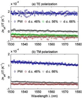
The results are plotted in Fig. 3over a 50 nm spectral
range, where each data point corresponds to the mea-sured shift of one transmission minimum. Solid lines are linear fits to the data. For TE polarization [Fig.3(a)], the TO coefficients of SWG waveguides with duty ratios of 46% and 56% are negative, while the TO coefficient of the photonic wire is positive, as expected. For a 66% duty ratio, the SWG waveguide is nearly athermal, consistent
with the small wavelength shifts observed in Fig. 2(c).
For this waveguide, the coefficients of the linear fit
function f ¼ aλ þ b are given by a ¼ −2:95 × 10−7nm−1
K−1and b ¼ 4:65 × 10−4K−1, which yields athermal opera-tion for a wavelength of 1576 nm. For TM polarizaopera-tion
[Fig. 3(b)], a positive TO coefficient is measured for
the photonic wire device, whereas the coefficient is ne-gative for the segmented SWG waveguides with these
Fig. 1. (Color online) (a) Schematic of an SU-8 clad silicon SWG waveguide. (b)–(d) SEM micrographs of SWG waveguides with duty cycles of 46%, 56%, and 66%. (e) Optical micrograph of an unbalanced MZI device with SWG sections. Arrows indicate the positions of wire-to-SWG waveguide couplers. The conti-nuation of the device beyond the field of view is indicated sche-matically on the right-hand side of the picture for clarity.
Fig. 2. (Color online) Temperature-dependent transmission spectra of MZI devices for different SWG duty ratios. A sign re-versal from negative to positive temperature-induced wave-length shifts is observed for increasing duty cycle.
Fig. 3. (Color online) Measured TO coefficient of photonic wire (PW) and SWG waveguides of various duty cycles (d.c.) indicated in the figure as functions of wavelength with linear fits (solid lines). (a) TE and (b) TM polarization.
duty cycles. While none of the measured SWG wave-guides exhibits athermal behavior for TM polarization, it is obvious from the observed sign reversal of the TO coefficient that athermal TM operation exists for a duty ratio between 66% and 100%.
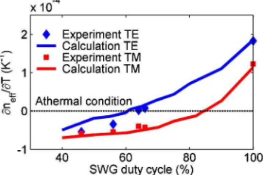
The values of the linear fits shown in Fig.3for the TO
coefficient dneff=dT at the wavelength λ¼ 1550 nm are
plotted as functions of SWG duty ratio in Fig. 4 for
both TE and TM polarizations (blue diamonds and red
squares). Our full data set plotted in Fig.4also includes
a waveguide with duty ratio of 64%, which, for clarity, is
not shown in Fig. 3. The experiment confirms the
ex-pected decrease of the TO coefficient with decreasing duty ratio, including sign reversal and near athermal be-havior for TE waveguides with a duty cycle of
approxi-mately 65%. Atλ ¼ 1550 nm, our lowest measured value
for the TO coefficient is 1:8 × 10⁻⁶K−1 for a duty ratio of 64%. The experimental data is compared to calculations
with the MIT photonic bands software [10], which is used
as a mode solver for the periodic waveguides. To find the TO coefficient numerically, we first calculate the
disper-sion (ω–k) diagram of the SWG waveguide using the
room-temperature values of the material refractive
in-dices (nSi¼ 3:476, nSU8¼ 1:58 and nSiO2 ¼ 1:444). The
waveguide effective index atλ ¼ 1:55 μm is obtained
di-rectly from the calculated dispersion, neff¼ ck=ω, where
c is the speed of light. The calculation is then repeated for the same structure at a different temperature. The refrac-tive indices of the constituent materials are changed from their room-temperature values to reflect a temperature increase of 20 K according to their respective TO coeffi-cients. From the results of the two calculations, the
de-rivative dneff=dT is determined. We overlaid the results
of this calculation with the experimental data in Fig. 4.
For the photonic wire waveguide, we obtain dneff=dT ¼
1:8 × 10⁻⁴K−1 and 1:2 × 10⁻⁴K−1 for TE and TM polariza-tion, respectively, in good agreement with the measured values. As the duty ratio of the SWG waveguides is
low-ered by increasing the gap size, we observe a transition from positive to negative TO coefficients for both polar-izations, as is also observed in the experiment. The zero crossing, corresponding to an athermal waveguide, oc-curs for a duty ratio of 61% for TE and 85% for TM. The higher duty ratio required for athermal operation for TM polarization is due to the fact that the electromag-netic boundary conditions cause the TM mode of our thin SWG waveguide to be more delocalized vertically than the TE mode, leading to a larger overlap with the SU-8 cladding above the waveguide for all duty ratios. To com-pensate for this effect, the volume ratio of the silicon ma-terial inside the composite waveguide core needs to be increased accordingly. Overall, the match of experimen-tal data and numerical calculations is excellent and vali-dates our strategy of mitigating the TO effect in optical waveguides by subwavelength patterning.
In conclusion, we have demonstrated that the sub-wavelength grating spatial averaging effect can be used to make temperature-independent waveguides with a composite core consisting of silicon and SU-8 polymer, compatible with standard silicon photonic wire wave-guides. Athermal behavior can be achieved for both TE and TM polarization, albeit for different SWG duty ra-tios. These results on engineering the TO waveguide properties using subwavelength gratings are thought to be a significant step forward toward developing tempera-ture-insensitive silicon photonic circuits.
References
1. A. Densmore, D.-X. Xu, P. Waldron, S. Janz, P. Cheben, J. Lapointe, A. Delâge, B. Lamontagne, J. H. Schmid, and E. Post, IEEE Photon. Technol. Lett. 18, 2520 (2006). 2. P. Cheben, J. H. Schmid, A. Delâge, A. Densmore, S. Janz,
B. Lamontagne, J. Lapointe, E. Post, P. Waldron, and D.-X. Xu, Opt. Express 15, 2299 (2007).
3. J.-M. Lee, D.-J. Kim, H. Ahn, S.-H. Park, and G. Kim, J. Lightwave Technol. 25, 2236 (2007).
4. W. N. Ye, J. Michel, and L. C. Kimerling, IEEE Photon. Technol. Lett. 20, 885 (2008).
5. J. Teng, P. Dumon, W. Bogaerts, H. Zhang, X. Jian, X. Han, M. Zhao, G. Morthier, and R. Baets, Opt. Express 17, 14627 (2009).
6. J.-M. Lee, D.-J. Kim, G.-H. Kim, O-K. Kwon, K.-J. Kim, and G. Kim, Opt. Express 16, 1645 (2008).
7. P. J. Bock, P. Cheben, J. H. Schmid, J. Lapointe, A. Delâge, S. Janz, G. C. Aers, D.-X. Xu, A. Densmore, and T. J. Hall, Opt. Express 18, 20251 (2010).
8. P. Rabiei, W. H. Steier, C. Zhang, and L. R. Dalton, J. Lightwave Technol. 20, 1968 (2002).
9. P. Cheben, P. J. Bock, J. H. Schmid, J. Lapointe, S. Janz, D.-X. Xu, A. Densmore, A. Delâge, B. Lamontagne, and T. J. Hall, Opt. Lett. 35, 2526 (2010).
10. http://ab‑initio.mit.edu/wiki/index.php/MIT_Photonic_Bands. Fig. 4. (Color online) Experimental and theoretical results for
the effective TO coefficient of SU-8 clad silicon SWG wave-guides as a function of grating duty cycle.