HAL Id: hal-02448419
https://hal.archives-ouvertes.fr/hal-02448419
Submitted on 5 Jan 2021
HAL is a multi-disciplinary open access archive for the deposit and dissemination of sci-entific research documents, whether they are pub-lished or not. The documents may come from teaching and research institutions in France or abroad, or from public or private research centers.
L’archive ouverte pluridisciplinaire HAL, est destinée au dépôt et à la diffusion de documents scientifiques de niveau recherche, publiés ou non, émanant des établissements d’enseignement et de recherche français ou étrangers, des laboratoires publics ou privés.
Charge injection in thin dielectric layers by atomic force
microscopy: influence of geometry and material work
function of the AFM tip on the injection process
Christina Villeneuve-Faure, K Makasheva, Laurent Boudou, G. Teyssedre
To cite this version:
Christina Villeneuve-Faure, K Makasheva, Laurent Boudou, G. Teyssedre. Charge injection in thin dielectric layers by atomic force microscopy: influence of geometry and material work function of the AFM tip on the injection process. Nanotechnology, Institute of Physics, 2016, 27 (24), pp.245702. �10.1088/0957-4484/27/24/245702�. �hal-02448419�
1
Charge injection in thin dielectric layers by Atomic Force
Microscopy: Influence of geometry and material work function of
the AFM tip on the injection process
C. Villeneuve-Faure, K. Makasheva, L. Boudou and G. Teyssedre
LAPLACE (Laboratoire Plasma et Conversion d’Energie) ; Université de Toulouse ; CNRS, UPS, INPT ; 118 route de Narbonne, F-31062 Toulouse cedex 9, France.
Abstract
Charge injection and retention in thin dielectric layers remain critical issues for the reliability of many electronic devices because of their association to a large number of failure mechanisms. To overcome this drawback a deep understanding of the mechanisms leading to charge injection close to the injection area is highly demanded. Even though the charge injection is extensively studied and reported in the literature to characterize the charge storage capability of dielectric materials, questions about charge injection mechanisms when using Atomic Force Microscopy (AFM) remain open. In this paper, a thorough study of charge injection by using AFM in thin plasma processed amorphous silicon oxynitride layers with properties close to that of thermal silica layers is presented. The study considers the impact of applied voltage polarity, work function of the AFM tip coating and tip curvature radius. A simple theoretical model was developed and used to analyze the obtained experimental results. The electric field distribution is computed as a function of tip geometry. The obtained experimental results highlight that after injection in the dielectric layer the charge lateral spreading is mainly controlled by the radial electric field component independently on the carrier polarity. The injected charge density is influenced by the nature of electrode metal coating (work function) and its geometry (tip curvature radius). The electron injection is mainly ruled by the Schottky injection barrier through field electron emission mechanism enhanced by thermionic electron emission. The hole injection mechanism seems to differ from the electron one in the dependence on the work function of the metal coating. Based on the performed analysis, it is suggested that for hole injection by AFM, pinning of the metal Fermi level with the metal-induced gap states in the studied silicon oxynitride layers starts playing a role in the injection mechanisms.
2
1. Introduction
Charging effect in thin dielectric materials was extensively studied since the 60’s of the last century because of the large scientific and technological interest to this physical phenomenon. Presently, the dielectric charging phenomenon is exploited in numerous applications, particularly in electret-based and non-volatile memory devices [1]. Charges accumulation in dielectric materials induces adverse effects on the response of the media, such as electric field strengthening, breakdown or electrostatic discharges, which represent failure issues for numerous systems. It is the case for example of radio-frequency MicroElectroMechanical Systems (RF-MEMS) [2]. Dielectric charging of RF-MEMS switches is the main cause of failure and low reliability of capacitive switches with electrostatic actuation. Due to the trapping of electrical charges on the surface and/or in the volume of the dielectric layer, the values of applied voltage for switch actuation are modified in a way that after a certain number of events the switch is out of control. Different strategies, related mainly to the nature of the dielectric layer (silica, silicon nitride, hafnium dioxide, tantalum pentoxide, etc.), have been adopted to overcome this yet resisting drawback. However, deep understanding of the mechanisms involved in charge injection and retention is crucial to improve reliability of devices and systems, and consequently to limit or even to avoid, their failure.Charge storage in insulating materials has received considerable attention during many years but it still represents great scientific challenges, largely due to the lack of knowledge on the specific mechanisms related to generation, transport and trapping of charges. Furthermore, when the layer thickness scales down below micrometer dimension, specific issues are superimposed [3]. For bringing new information on these processes, development of diagnostic means of charging state, adapted to characterization of thin layers (thickness of few tens of nanometers), is highly demanded. Classical space charges measurement techniques, based on acoustic [4] or thermal [5] perturbation, fail to characterize thin dielectric films (thickness of less than a few microns) due to their limited in-depth spatial resolution which is of the order of a few microns at most. To attain the nanoscale level, techniques derived from Atomic Force Microscopy (AFM) have naturally emerged offering the possibility to localize injected charges and to probe the resulting modifications in the electrostatic field.
During the past decade Electrostatic Force Microscopy [6-8] (EFM) and Kelvin Force Microscopy [3, 7, 9] (KFM) were extensively used to study charge injection and retention in thin dielectric films. From experimental point of view, the charge injection phenomenon is strongly influenced by the injection conditions: injection in contact or dynamic mode [10], environment (humidity or gas nature) [3, 7], surface treatment [10], and measurement distance
3
[11] (in case of lift mode). Even though the dielectric charging effects were extensively investigated experimentally, the underlying physical phenomena are still marginally discussed in the literature. The difficulties often stem from the fact that the electric field is very high and highly diverging, and that the charging procedures are quite difficult to model, e.g. charging achieved in taping mode. Up to now only few mechanisms were proposed to explain the charge injection in thin dielectric films. Injection by corona discharge [12] is commonly evoked in the literature as the main mechanism in analogy with the most widely applied technique for dielectric charging. However, recent theoretical calculations, and the following analysis, demonstrate that corona discharge cannot develop in so small tip-to-sample distances, making it impossible to be considered as mechanism at the origin of charge injection in AFM [13]. It is rather an electric field dependent mechanism to be seek to explain the dielectric charging by AFM, in particular the field electron emission enhanced by thermionic electron emission [13]. Moreover, current measurements during charge injection reveal a behavior close to Fowler-Nordheim mechanism [14, 15]. Most of the studies on dielectric charging by AFM focus on the charges retention capabilities of materials [3, 12]. The influence of tip characteristics (geometry of the tip and work function of the coating material) is rarely taken into account to better understand the charge injection mechanisms. Sun et al [16] briefly addressed the influence of the material work function of the AFM tip on the charge injection, by comparing features from two tips with different coatings. However there was no consideration of the tip geometry (which actually controls the electric field) or the voltage polarity. Indeed, the AFM tip geometry is an important parameter which indicates that different mechanisms [13] are involved in the charge injection process since electrons and holes exhibit different injection and decay rates [17].
This study addresses the physical phenomena involved during AFM charge injection in thin dielectric layers. Particularly, it reveals the influence of tip radius and tip work function on the electron and hole injection through KFM measurements. After a quick presentation of the experimental conditions, electric field simulation, using Finite Element Model (FEM), is presented. Then, the experimental results obtained by KFM on plasma-processed amorphous silicon oxynitride thin layers exploring AFM tips with different geometries and metal coatings, i.e. different work functions, are presented and discussed using the results from the electric field simulation to identify the mechanisms involved in electron/hole injection and their lateral spreading.
5
2. Experimental part
To investigate charge injection in thin dielectric layers, a structurally well characterized material is needed. Amorphous silicon oxynitride layers (a-SiOxNy:H, x < 2, y < 1) with very low nitrogen content (only 4 at.% for all samples) and structural and electrical properties close to a thermal silica layer were selected for this study. They were elaborated by Pulsed Plasma Enhanced Chemical Vapor Deposition (PPECVD) [18]. Our choice to probe plasma deposited thin layers is based on the versatility of the plasma process and its compatibility with microelectronic technology, which makes the study useful for many different applications. The a-SiOxNy:H layers were deposited on Au/Ti metallized Si (100) 4"-wafers in the plasma sustained by a capacitively-coupled radiofrequency (RF) discharge at frequency of
f = 13.56 MHz with power of 5 W. In the so-described structure the Ti-layer was used as
adhesive layer between the Au-layer and the Si-substrate. The RF discharge was modulated with square pulses of period Tp = 400 ms and pulse width of 100 ms. The gas mixture
contained SiH4 (1.2 sccm, where sccm stands for standard cubic centimeters per minute at standard temperature and pressure), N2O (120 sccm) and He (80 sccm, equivalent to 40% of the total gas flow). The total gas pressure used for deposition was p = 65 Pa. The substrate temperature was kept to 300°C during the deposition process.
The layer thickness and its optical properties were determined by spectroscopic ellipsometry measurements in the spectral range 250-850 nm. A Sopra GES-5 ellipsometer was used. Detailed description of the applied procedure to acquire the spectra is given in reference [19]. Simulation of the recorded spectra was performed with Winelli software [20] provided by Sopra. Forouhi-Bloomer dispersion law [21] was applied for spectra processing. This approximation provides information on the layer thickness and its optical properties (n – refractive index and k – extinction coefficient). To study the charge injection we have used 40 nm-thick a-SiOxNy:H layers (refractive index, n = 1.49 ± 0.01 at = 632.8 nm and relative dielectric permittivity, r = 3.90 ± 0.05 at 1 kHz and room temperature determined by
spectroscopic ellipsometry and dielectric spectroscopy measurements, respectively). More information on the structural and electrical characterization of these dielectric layers is given elsewhere [18, 19].
6
Figure 1. SEM images of silicon AFM tips with (a) Pt and (b) diamond coating.
AFM measurements were performed using a Bruker Multimode 8 apparatus. Charges implantation protocol and ambient environment were well controlled in order to ensure results repeatability. AFM silicon tips with different coating materials, as provided by Bruker and NanoSensor, were used to investigate the influence of injection conditions, especially the influence of tip work function and geometry on the injected charges. The charging step was achieved in contact mode (contact force set to 20nN) by applying positive or negative DC bias between ±5V and ±25V to the AFM tip during 1min, the silicon wafer back side being grounded. The Au/Ti layer between the silicon substrate and the dielectric layer remains at floating potential. Moreover, a controlled environment, without humidity and under N2 atmosphere, was used avoiding thus charge dissipation due to water layer adsorbed on the sample surface. After the charging step, the same AFM tip was used to probe the surface potential by Amplitude Modulation KFM with 5nm-lift. The spring constant was estimated using Thermal Tune mode and was monitored during measurements to control accurately the contact force during injection. As the tip properties are crucial for our study, each tip was previously characterized using Scanning Electron Microscopy (SEM) to determine the tip curvature radius. Figure 1 shows SEM images of AFM silicon tips with different coatings emphasizing important differences in terms of surface morphology and curvature radius. The characteristics of all tips used in this study are summarized in Table 1.
Table 1. AFM tip characteristics
Item Pt Co PtSi D
Coating on silicon Platinum Cobalt PtSi alloy Diamond
Work function - m 5.64 eV [22] 5.00 eV [22] 4.80 eV [23]
Depends on doping (around 5.5eV)
7
46 nm 46 nm × ×
× 118 nm × 128 nm
3. Electric field modeling
To identify physical mechanisms involved in charge injection using AFM tip, electric field modeling is required. A simple model describing the AFM tip as a truncated cone of 10µm- height with 14° degrees aperture angle, and ending with a semi-spherical apex (of curvature radius Rc) was used. It corresponds to classical AFM tip shape used for modeling [24]. The tip is supposed to be surrounded by air box (of dimensions large enough to avoid edge effects) and in contact with the dielectric a-SiOxNy:H layer, of 40 nm in thickness. The relative dielectric permittivity of a-SiOxNy:H equals 3.9, as measured by dielectric spectroscopy [18] and that of the air is taken as 1. The potential is applied on the tip surface and the dielectric back side is supposed at reference potential.
In order to compute the electric field distribution in air and in the dielectric layer, a 2D-axisymmetric finite-element model using COMSOL Multiphysics® was developed. Mesh was refined and optimized close to the contact point to improve calculation accuracy. The dielectric layer was supposed free from electrical charges. The Poisson's equation was solved in air and in the dielectric layer to determine the potential distribution. Without charges, it is in the form:
0
divEr . (1)
The electric field Er derives from the potential:
Er grad V . (2)
Typical boundary conditions for the described configuration were applied. No charge conditions (zero potential) are applied on the free boundaries of the simulation box. These conditions ensure no edge effects.
Figure 2(a) represents the equipotential lines and the electric field intensity for 10V applied on a 27nm-radius tip. The distribution of the axial component of electric field Ez is
depicted in figure 2(b). As expected, the electric field is enhanced close to the AFM apex. The evolution of Ez as a function of the position in depth of the dielectric layer (along the vertical
axis for r = 0) is represented in figure 2(d) for different tip curvature radii and applied potential of 10V. Close to the dielectric surface, the electric field is substantially enhanced compared to a plane-plane configuration (2.5 × 10⁸ V/m for the above given conditions, represented by the dot line in figure 2(d)). This field intensification increases when the tip curvature radius is smaller. The ratio between electric field intensity at the tip and that at the ground varies with
8
factors from about 3.5 to 1.6 when the tip curvature radius changes from 27 to 120nm. The calculated electric field strengths at the contact point are not far from the highest applied electric field (1.5 108 V/m) in current measurements performed on Metal/Insulator/Metal capacitors containing the studied oxynitride layers where no breakdown appeared [18]. Besides, KFM measurements performed at the same location after charges dissipation exhibit no modifications either of the surface topography or of the surface potential, whereas this should be the case when local breakdown occurs [25].
The radial contribution of the electric field Er is depicted in figure 2(c) for 10V applied
on the 27nm-radius tip. It can be seen that the radial field contribution both in air and in the dielectric is quite significant and cannot be neglected in respect to the axial contribution of the electric field when considering the electric field intensity. The Er distribution at the
dielectric/air interface (z = 0) is represented in figure 2(e) for the same applied potential and different tip curvature radii. Note that there is continuity of the radial contribution of the field at the air/dielectric interface, contrary to the case of the axial contribution. The radial electric field maximum value and position are strongly influenced by the tip curvature radius. Indeed, when the tip curvature radius decreases, the maximum electric field increases and occurs at closer distance to the contact point. In the following, experimental results are compared with the axial electric field at the injection point and with the maximum value of the radial electric field component at dielectric/air interface.
9 -40 -30 -20 -10 0 -6 -5 -4 -3 -2 -1 -6 -5 -4 -3 -2 -1 Rc = 27 nm Rc = 46 nm Rc = 120 nm Depth in dielectric z (nm) Ez ( r = 0 ) (10 8 V /m ) (d) -200 -100 0 100 200 0.0 0.5 1.0 1.5 2.0 2.5 3.0 Rc = 27 nm Rc = 46 nm Rc = 120 nm Radial position r (nm) Er ( z = 0 ) (10 8 V /m ) (e)
Figure 2. Spatial distribution of the computed electric field: (a) equipotential lines and electric field intensity; (b) axial contribution Ez and (c) radial contribution Er of the electric field for 10V applied on 27nm-curvature radius
AFM tip. Impact of tip curvature radius on the field distribution: comparison of (d) Ez(r=0) and (e) Er(z=0) cross
sections with 10V applied to AFM tips of different curvature radii.
4. Experimental results
Charge injection was performed under tip bias varying from -25V to 25V in 5V steps applied for 1min. For each new value of the bias voltage the charge injection was achieved on a new position on the a-SiOxNy:H layer away from a previously charged point not to suffer any influence. KFM profiles were recorded immediately after voltage application, along a line crossing the injection point. Figure 3 represents classical cross-section over bell-like shape potential, which is obtained after local charging of the thin dielectric layer [19]. This profile exhibits Gaussian shape and is exploited for extraction of three parameters relevant to our study: (i) the maximum potential, Vm, in respect to surface reference potential which is measured at the injection point; (ii) the peak full width at half maximum (FWHM) which reflects the lateral spreading of injected charges; and (iii) the area under the potential profile Is, which represents to a first approximation the quantity of stored charges in the dielectric layer [26]. In the following, the impact of AFM tip geometry, tip coating and applied bias on these three parameters is studied aiming at an identification of the charge injection mechanisms.
0 1 2 3 4 5 -1 0 1 2 3 Vm Position (µm) K F M p o te n ti a l (V ) FWHM -1 0 1 2 3
10
Figure 3. KFM profile obtained on 40nm-thick a-SiOxNy:H layer after charging for 1min at 25V using Pt-coated
AFM tip with curvature radius Rc = 27nm.
4.1. Lateral charge spreading
Figure 4(a) represents the evolution of the FWHM of the potential profiles as a function of the applied bias for different tips. As the FWHM reflects the charge spreading in the dielectric layer this parameter is closely related to the structural properties of the studied dielectric layers. The selected, for this study, a-SiOxNy:H thin layers with properties close to thermal silica offer the possibility to inject measurable quantity of charges [19] however, strongly limiting the lateral charge spreading. The surface potential profile remains almost unchanged (broadening of less than 5%) over the charge injection step. It means that the variation of FWHM presented on figure 4(a) is solely due to the applied bias and the properties of different tips. First of all, the FWHM increases continuously with the applied bias independently of the carrier nature (positive or negative bias). Moreover, the FWHM behavior depends only on the tip radius. The nature of the tip coating seems to have no influence. The fact that FWHM varies with tip radius and injection bias without effect of the tip coating or charging polarity points towards geometrical features of the measurement conditions including field magnitude. As the dielectric layer is relatively thin in respect to the measured FWHM, it is expected that the position of the charges in the depth of the dielectric layer has little influence on the measured FWHM, i.e. the injected charges are trapped at the vicinity of the injection point. Therefore, we have tentatively put in relation the width of the potential profile and the computed radial component of the electric field for the same tip radius and applied bias. -30 -20 -10 0 10 20 30 200 400 600 800 Pt - Rc=27nm PtSi - Rc=27nm Pt - Rc=46nm Co - Rc=46nm Co - Rc=118nm D - Rc=128nm Applied bias (V) F W H M ( n m ) 200 400 600 800 (a) 0 1 2 3 4 5 6 200 400 600 800 Pt - Rc=27nm PtSi - Rc=27nm Pt - Rc=46nm Co - Rc=46nm Co - Rc=118nm D - Rc=128nm Er max (z = 0) (108 V/m ) F W H M ( n m ) 200 400 600 800 (b)
Figure 4: Evolution of the FWHM of KFM profile as function of (a) injection bias and (b) lateral electric field for different AFM tips.
11
Figure 4(b) represents the variation of FWHM as a function of the maximum value of the radial electric field component computed according to the model presented in the previous section for each one of the couples: applied bias to the tip and its curvature radius. A good correlation is observed between the FWHM and the maximum of the radial electric field. Indeed, the FWHM of the potential spot increases when the radial electric field increases. The charge spot broadening is less pronounced for tips with large curvature radii, which most probably is linked to the degradation of the lateral resolution for these tips. The tip diameter in this case approaches the potential spot dimensions. These results emphasize that charge lateral spreading is mainly driven by the radial electric field, independently from the charges nature. To go deeper into the understanding of this phenomenon a more detailed theoretical model taking into account the radial electric field modifications induced by the injected charges and description of the available charge traps in the dielectric thin film is required. However, as a first approximation our results show that the broadening of the potential profile is mainly driven by the radial electric field. Most likely the trapping of the injected charges prevents from further lateral spreading.
The FWHM vs. bias curves appear symmetrical with bias polarity, cf. figure 4(a). This is not a necessarily expected behavior since the dispersion of positive and negative charges on the sample surface might be different. Reports on other materials like SiO2 or PMMA [10] with non-symmetric FWHM point towards surface carrier conductivity which can be affected by surface pollution (water layer for example). In the dry atmosphere conditions of our study, surface conductivity is avoided and the behavior should be linked to the intrinsic properties of the a-SiOxNy:H dielectric layer. Consequently, in the studied a-SiOxNy:H thin layers, for high electric fields (>108 V/m), positive and negative carriers exhibit quite the same lateral transport features.
4.2. Charge injection efficiency
To investigate charge injection efficiency in thin dielectric layers two parameters are considered: (i) AFM tip (electrode) metallic coating (metal work function) and (ii) tip curvature radius. These two parameters are involved in the theory of field emission in intense electric fields established by Fowler and Nordheim [14]. Figure 5 emphasizes the influence of tip curvature radius on the variation of the measured KFM maximum potential (Vm) and on the integrated potential (Is, the area of KFM profile considered as a measure of the density of stored charges) as a function of applied bias for Pt-coated tip. As shown on figure 5(a), the maximum potential increases linearly with the applied bias. The maximum potential is higher
12
for smaller tip curvature radius. Figure 5(b) confirms the increase in stored charge amount with decreasing the tip curvature radius. The integrated potential is symmetrical when the bias polarity is reversed. Consequently, for Pt-coated electrode, the injected charge amount is independent from the bias polarity. The increase in tip curvature radius induces significant decrease in the injected charge amount.
-30 -20 -10 0 10 20 30 -4 -2 0 2 4 (b) Rc=27nm Rc=46nm Vm ( V ) Applied bias (V) (a) -30 -20 -10 0 10 20 30 0 1 2 3 Is ( V µ m ) Applied bias (V)
Figure 5. Evolution of (a) maximum potential Vm and (b) integrated potential profile Is as a function of injection
bias for Pt-coated AFM tips with different curvature radii.
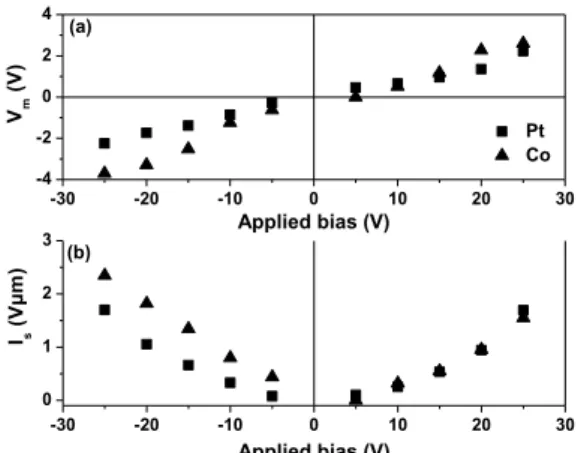
Figure 6 emphasizes the influence of metallic coating (metal work function) on the evolution of maximum potential and integrated potential profile as a function of applied bias for a 46nm-curvature radius tip. As shown on figure 6(a), the maximum potential increases linearly with the applied bias but its behavior strongly depends on the bias polarity. Indeed, for positive bias on the tip, the maximum potential scales up linearly without being influenced by the metal coating nature whereas, for negative applied bias, the maximum potential evolution depends substantially on the metal coating determining a steeper slope of the curve for Co- compared to the Pt-coated tip. Figure 6(b), confirms the above observations and points out that, contrary to the Pt-coated tip, the integrated potential profile obtained with the Co-coated tip is not symmetric with respect to the positive and negative applied bias polarities. For positive applied bias, the injected charge density is independent on the metal coating, whereas for negative bias, the injected charges amount is larger for the Co- than for the Pt-tip. The origin of this effect can be found in the difference of the work functions between the two metal coatings of the AFM tip. To confirm this evolution a more systematic study on the influence of electrode work function on the charges density is proposed in the next section.
13 -30 -20 -10 0 10 20 30 -4 -2 0 2 4 (a) Pt Co Vm ( V ) Applied bias (V) (b) -30 -20 -10 0 10 20 30 0 1 2 3 Is ( V µ m ) Applied bias (V)
Figure 6. Evolution of (a) the maximum potential Vm and (b) the integrated potential profile Is as function of the
injection bias for Pt- and Co-coated AFM-tips (curvature radius fixed to 46nm).
The electrostatic modeling presented in section 3 shows that the axial electric field represents the main contribution to the electric field. Therefore, the integrated potential profile Is for different metal coatings and tip radii obtained for negative applied bias to the tip is presented in figure 7(a) as a function of the axial electric field computed at the injection point. The integrated potential profile Is appears roughly proportional to the electric field strength at the injection point and the slope of this dependence is steeper when the work function of the metallic coating is lower. The proportionality between Is and applied bias V is probably fortuitous since injection laws in general are non-linear in field and the field is diverging in the analyzed situation, with the existence of a triple point around the injection point. In addition, the radial component of the electric field favors lateral spreading of the injected charges. The greatest contribution of the radial electric field appears at a finite distance from the injection point (r = 0) and the position of the maximum along with the magnitude are substantially dependent on the tip curvature radius (figure 2(e)). For these reasons, it is difficult to evaluate charge amount vs. applied bias for inferring injection mechanism. However, the impact of the metal work function is addressed in the discussion.
The shape of the Is vs V curves is different for positive applied injection bias to the AFM tip. Indeed, as shown on figure 7(b), for Co- and Pt-coatings the integrated potential profile scales up linearly with the electrical field offering a reduced influence of the tip coating. The dependencies on the metal coating work function get closer to each other, even showing a tendency to invert. Exception is observed for the PtSi-coated tip only which is most probably related to the kind and doping degree of Si in the alloy, unfortunately not reported in the AFM tip data sheet. However, the results shown in figure 7 confirm that the electric field has quite the same influence on the hole injection height barrier as on the electron one, but the
14
dependence on the metal work function differs. To clarify this last point we have performed an analysis treating the studied silicon oxynitride layers as wide-band-gap semiconductors.
0 5 10 15 0 1 2 3 PtSi - m=4.8eV Co - m=5.0eV Pt - m=5.64eV Ez (r = 0) (108 V/m ) Is ( V µ m ) (a) 0 1 2 3 0 5 10 15 0 1 2 3 4 5 PtSi Co Pt Ez (r = 0) (108 V/m ) Is ( V µ m ) (b) 0 1 2 3 4 5
Figure 7. Evolution of the area under the potential profile Is as function of the computed axial electric field
component for different metal work functions for (a) negative injection bias and (b) positive injection bias in a-SiOxNy:H thin layer. The lines in the graph are shown as guide to the eye.
6. Discussion
The physical situation that arises in this study is a contact between metal and dielectric layers. The transport properties at the metal-semiconductor (dielectric) interface, usually called MS-interface, are generally considered in terms of Schottky barrier height (SBH). Accordingly, the density of injected charges is determined by the SBH. When a negative bias is applied to the tip, one considers that electrons are injected in the silicon oxynitride layer. The injection barrier height ϕe is given by [27]:
3 0 4 e m r e E , (3)
where ϕm is the metal work function, χ is dielectric layer electron affinity, e is the elementary
charge, εr is the relative permittivity of the dielectric layer and ε0 is the vacuum permittivity. Given the constant character of parameters related to the silicon oxynitride layer, a-SiOxNy:H, relation (3) predicts that the injection barrier decreases when the electric field increases and/or the metal work function decreases. Considering the measured for the a-SiOxNy:H relative dielectric permittivity εr = 3.9 [18] and electron affinity of silica layers as reported in the
literature = 0.9 eV [28] we estimate from relation (3) a reduction of the injection barrier height of 0.27 eV for the lowest applied field of 2.0 108 V/m and of 0.74 eV for the highest applied field of 1.5 109 V/m. For a given value of the electric field the reduction of the injection barrier height leads to an easier injection of the electrons in the dielectric layer. This results in a higher density of injected charges as observed in this study (figure 7(a)). When the
15
metal coating has lower metal work function, i.e. Co-coated tip versus Pt-coated tip, the injection is further enhanced. As far as the injection mechanism is concerned its identification requires analysis considering also the temperature as the injection barrier is involved in different injection mechanisms like thermionic emission or field electron emission, or the mutual action of both emissions [29]. For the range of electric field variation studied in this work and based on the methodology described by Murphy and Good [29], the domains of action of thermionic and field electron emissions, the intermediate region and their limits were studied and reported for Co- and Pt-coatings in reference [13]. While the electric field dependence acts on the shape of the injection barrier at the surface, the temperature dependence occurs at the Fermi distribution function of the free electron gas in the metal. The charge injection in this work was performed at room temperature. For electric field strengths up to 6.4 108 V/m the electrons are injected in the silicon oxynitride layer due to the mutual action of thermionic and field electron emissions. The domain of pure field electron emission applies for higher electric fields. As predicted earlier [29] and observed here the transition between different injection mechanisms is smooth (figure 7(a)).
Figure 8. Energy band diagram for metal-dielectric interface. The metal is described by its Fermi level (EFm) and
its work function ϕm. MIGS are described by the charge neutrality level ϕCNL. The dielectric is described by its
valence EV and conduction EC levels.
However, application of a positive bias cannot be analyzed only on the basis of pure Schottky injection mechanism although the electric field strength is high. The region created on the MS-interface should also be considered. Without loss of generality, when a positive bias is applied to the AFM tip (figure 7(b)) the charge injection barrier height at the metal-oxide interface is rather described in the literature by the theory of metal-induced gap states (MIGS) [30]. These states are predominant donorlike if they are close to the dielectric valence
16
band - EV and acceptorlike when they are close to the conduction band - EC (figure 8). The energy level in the band gap where the inversion occurs is called charge neutrality level - ECNL. Generally though, when a metal and semiconductor (oxide layer) are in contact they form an interface where charge transfer arises between the metal and interface states lying in the semiconductor/dielectric band gap. The charge transfer creates a dipole which reduces the SBH and consequently modulates the influence of the metal on injection. As shown in figure 8, when the metal Fermi level is close to the EV and MIGS are close to the EC the electron injection will be driven by the metal work function and the hole injection by MIGS.
Using the MIGS model the potential barrier height ϕh for hole injection can be
expressed by the following relation:
h Eg S m CNL CNL
, (4)
where Eg is the electronic gap of the dielectric layer and ϕCNL is the charge neutrality level
measured from vacuum level which depends on the dielectric material properties. S is a dimensionless slope of barrier height to metal work function. It is related to the density of MIGS and their extension in the dielectric gap describing thus the pinning of the Fermi level of the metal with the MIGS and the degree of screening induced by the interfacial states [27]. It was shown previously that the pinning parameter S correlates with the electronic part of the dielectric constant () [31] and empirically obeys the relation [32]:
2 1 1 0 1 1 S . , (5)where is the high frequency limit of the dielectric constant. For S equals 1, MIGS have no
influence on hole injection and for S equals 0, injection is ruled only by MIGS [33]. Concerning the a-SiOxNy:H layer under study the measured by ellipsometric spectroscopy value of the electronic part of the dielectric constant is = 2.24. Applying the relation (5) one finds the pinning parameter S equals 0.867. This value is consistent with values reported in the literature for silica layers [28, 31-33] as the used a-SiOxNy:H layer has dielectric properties close to thermal silica. The obtained value for the pinning parameter indicates rather low influence of the interfacial states on the hole injection, i.e. the work function dependence is not screened by the interfacial states, which actually does not explain the results obtained when a positive bias is applied on the AFM tip (figure 7(b)). Although physically sound, the MIGS theory has some drawbacks, like for example the point that it describes the semiconductor (dielectric) part without considering the image charge created in the metal. The CNL does not apply to the entire interface region. It rather refers to the
17
semiconducting part only. It assumes that the net charge due to the occupation of surface states is determined only by the position of the Fermi level at the surface. The CNL is defined as the one that coincides with the Fermi level position, no distribution is assumed.
A recent theory [34, 35] based on the polarization of the chemical bonds at metal semiconductor interfaces could quantitatively account for the experimentally observed strength of Fermi level pinning (S parameter) without regard to the actual distribution of gap states. It goes beyond the MIGS theory, considering formation of a dipole, called Schottky dipole, which is formed from the net charge resulting from the gap states and its image charge in the metal. Only considering a chemical bonding at the MS-interface a coherent explanation of the Fermi level pinning effect, on the one hand, and the experimentally observed dependence of the SBH on interface structure, on the other hand, can be provided.
5. Conclusion
Influence of AFM tip geometry (curvature radius of the tip) and metal coating (work function) on the charge injection in thin dielectric amorphous silicon oxynitride layers was investigated experimentally. A theoretical model was developed to support the analysis of the obtained results. Results emphasize that the charge lateral spreading is driven by the radial contribution of the electric field. Moreover, it was shown that in a-SiOxNy:H thin layers both carriers, electrons and holes, obey the same lateral transport processes. Concerning charge injection mechanisms, the injected charge amount is influenced by the nature of electrode metal coating (work function) and its geometry (tip curvature radius) which modify the applied electric field. The charge behavior varies as a function of the carrier nature. The electron injection is mainly ruled by the Schottky injection barrier through field electron emission mechanism enhanced by thermionic electron emission. The amount of injected charges increases with increasing the electric field intensity and decreasing the work function of the AFM tip metal coating. It is larger when the charge injection is performed with AFM tips with smaller curvature radii. However the hole injection mechanism seems to differ from the electron one in the dependence on the work function of the metal coating. The MIGS theory fails to describe correctly the charge injection mechanism for hole carriers in the studied a-SiOxNy:H thin layers expressing an experimentally obtained pinning parameter not much lower than unity. Further studies will be directed to elucidation of this last observation to better understand the charge transfer at the interface between two very thin metal/dielectric layers
18
when using AFM. A direction to explore is the recently developed theory based on the polarization of the chemical bonds at metal semiconductor interfaces.
Acknowledgments
The authors acknowledge support from the UMS Raymond Castaing of the University of Toulouse and Mr. Stéphane Le Blond du Plouy for the SEM observations. This work is financially supported by the Agence Nationale de la Recherche in France, project ANR-InTail under contract ANR-AA-PBLI-II-2011 and the Région Midi-Pyrénées.
References
[1] Normand P, Kapetanakis E, Dimitrakis P, Skarlatos D, Tsoukalas D, Beltios K, Claverie A, Benassayag G, Bonafos C, Carrada M, Cherkashin N, Soncini V, Agarwal A, Sohl C and Ameen M 2003 Effects of annealing conditions on charge storage of Si nanocrystal memory devices obtained by low-energy ion beam synthesis Microelectronic
Engineering 67 629–634
[2] Witvrouw A, Tilmans H A C and De Wolf I 2004 Materials issues in the processing, the operation and the reliability of MEMS Microelectronic Engineering 76 245–257
[3] Rezende C A, Gouveia R F, da Silva M A and Galembeck F 2009 Detection of charge distribution in insulator surfaces J. Phys.: Condensed Matter 21, 263002
[4] Maeno T and Fukunaga K 1996 High-resolution PEA charge distribution measurement system IEEE Trans. Dielectr. Electr. Insul. 3 754–757
[5] Mellinger A, Singh R, Wegener M, Wirges W, Gerhard-Multhaupt R and Lang S B 2005 Three-dimensional mapping of polarization profiles with thermal pulses Appl.
Phys. Lett. 86 082903
[6] Stern J E, Terris B D, Mamin H J and Rugar D 1988 Exposition and imaging of localized charge on insulator surfaces using force microscope Appl. Phys. Lett. 53, 2717–2719
[7] Marchi F, Dianoux R, Smilde H J H, Mur P, Comin F and Chevrier J 2008 Characterisation of trapped electric charge carriers behaviour at nanometer scale by electrostatic force microscopy J. Electrostatics 66 538–547
19
[8] Lambert J, de Loubens G, Guthmann C and Saint-Jean M 2005 Dispersive charge transport along the surface of an insulating layer observed by electrostatic force microscopy Phys. Rev. B 71 155418
[9] Morita S, Uchihashi T, Okamoto K, Abe M and Sugawara Y 2005 Microscale contact charging on silicon oxide NATO Science Series II: Math. Phys. Chem. 186 289–308 [10] Silva-Pinto E and Neves B R A 2010 Charge injection on insulators via SPM
techniques: towards data storage devices J. Nanosci. Nanotechnol. 10 4204-4212
[11] Zaghloul U, Bushan B, Pons P, Papaioannou G J, Coccetti F and Plana R 2011 On the influence of environment gases, relative humidity and gas purification on dielectric charging/discharging processes in electrostatically driven MEMS/NEMS devices
Nanotechnology 22, 035705
[12] Morita S, Sugawara Y and Fukano Y 1993 Atomic Force Microscope combined with scanning tunneling microscope Jpn. J. Appl. Phys. 32 2983-2988
[13] Makasheva K, Villeneuve-Faure C, Laurent C, Despax B, Boudou L and Teyssedre G 2015 Dielectric charging by AFM in tip-to-sample space mode: overview and challenges in revealing the appropriate mechanisms Nanotechnology 26, 295704
[14] Fowler R H and Nordheim L 1928 Electron emission in intense electric fields Proc. R.
Soc. London, Ser. A 119 173-181
[15] Ando A, Hasunuma R, Maeda T, Sakamoto K, Miki K, Nishioka Y and Sakamoto T 2000 Conducting atomic force microscopy studies on local electrical properties of ultrathin SiO2 films Appl. Surf. Sci. 162, 401-405
[16] Sun Z, Wang X, Song W and Lei Q 2013 A research on the Surface Charge with Different Coating Tip by Electrostatic Force Microscope Annu. Rep. IEEE Conf. Electr.
Insul. Dielectr. Phenomena (CEIDP), 295-297 DOI: 10.1109/CEIDP.2013.6748244
[17] Morita S and Sugawara Y 2001 Microscopic contact charging and dissipation Thin
Solid Films 393 310-318
[18] Makasheva K, Despax B, Boudou L and Teyssedre G 2012 Dielectric layers for RF-MEMS switches: Design and study of appropriate structures preventing electrostatic charging IEEE Trans. Dielectr. Electr. Insul. 19 1195-1202
[19] Villeneuve-Faure C, Makasheva K, Bonafos C, Despax B, Boudou L, Pons P and Teyssedre G 2013 Kelvin force microscopy characterization of charging effect in thin a-SiOxNy:H layers deposited in pulsed plasma enhanced chemical vapor deposition process by tuning the silicon environment J. Appl. Phys. 113, 204102
20
[21] Forouhi A R and Bloomer I 1986 Optical dispersion relations for amorphous semiconductors and amorphous dielectrics Phys. Rev. B 34 7018–7026
[22] Lide D R (ed) 2008 CRC Handbook on Chemistry and Physics, 89th rev. edn (Boca Raton, FL: CRC Press) pp 112–4
[23] Niranjan M K, Zollner S, Kleinman L and Demkov A A 2006 Theoretical investigation of PtSi surface energies and work functions Phys. Rev. B 73 195332
[24] Boularas A, Baudoin F, Villeneuve-Faure C, Clain S and Teyssedre G 2014 Multi-dimensional modelling of electrostatic force distance curve over dielectric surface: Influence of tip geometry and correlation with experiment J. Appl. Phys. 116 084106 [25] Porti M, Nafria M, Blüm M C, Aymerich X and Sadewasser S 2003 Atomic force
microscope topographical artifacts after the dielectric breakdown of ultrathin SiO2 films
Surface science 532 727–731
[26] Stevens G C and Blaird P J 2005 Nano- and Meso-measurement methods in the study of dielectric, IEEE Trans. Dielec. Insul. 12, 5.
[27] Kao K-C and Hwang W 1981 Electrical transport in solids (Pergamon Press: New York)
[28] Robertson J 2000 Band offset of wide-band-gap oxides and implication for future electronic devices J. Vac. Sci. Technol. B 18 1785-1791
[29] Murphy E L and Good Jr R H 1956 Thermionic Emission, Field emission, and the Transition Region Phys. Rev. 102 1464-1473
[30] Heine V 1965 Theory of Surface States Phys. Rev. 138 1689-1696
[31] Tersoff J 1984 Schottky Barrier Heights and the Continuum of Gap States Phys. Rev.
Lett. 52 465-468
[32] Mönch W 1987 Role of Virtual Gap States and Defects in Metal-Semiconductor Contacts Phys. Rev. Lett. 58 1260-1263
[33] Yeo Y C, King T J and Hu C 2002 Metal-dielectric band alignment and its implications for metal gate complementary metal-oxide-semiconductor technology J. Appl. Phys. 92 7266-7271
[34] Tung R T 2001 Formation of an electric dipole at metal-semiconductor interfaces Phys.
Rev B 64 205310
[35] Tung R T 2014 The physics and chemistry of the Schottky barrier height Appl. Phys.