HAL Id: hal-02473107
https://hal-amu.archives-ouvertes.fr/hal-02473107
Submitted on 10 Nov 2020
HAL is a multi-disciplinary open access archive for the deposit and dissemination of sci-entific research documents, whether they are pub-lished or not. The documents may come from teaching and research institutions in France or abroad, or from public or private research centers.
L’archive ouverte pluridisciplinaire HAL, est destinée au dépôt et à la diffusion de documents scientifiques de niveau recherche, publiés ou non, émanant des établissements d’enseignement et de recherche français ou étrangers, des laboratoires publics ou privés.
Jean-Luc Autran, Daniela Munteanu
To cite this version:
Jean-Luc Autran, Daniela Munteanu. Atmospheric Neutron Radiation Response of III-V Binary Com-pound Semiconductors. IEEE Transactions on Nuclear Science, Institute of Electrical and Electronics Engineers, 2020, 67 (7), pp.1428-1435. �10.1109/TNS.2020.2971611�. �hal-02473107�
Abstract—This works is a first tentative to explore, by simulation, the radiation response of III-V binary compound semiconductors subjected to high energy atmospheric neutrons. The study focuses on the radiation response of eight III-V materials: GaAs, AlAs, InP, InAs, GaSb, InSb, GaN and GaP. For each semiconductor, the interaction rates of a bulk material target exposed to a neutron source mimicking the atmospheric neutron spectrum at sea-level is evaluated both from direct calculation using nuclear cross section libraries and by Geant4 simulations. These latter are also used to investigate in detail the reaction rates per type of reaction (elastic, inelastic, nonelastic) and to classify all the neutron-induced secondary products considering their atomic number and energy. Implications for single event effects are analyzed and discussed, notably in terms of electrical charge deposited in the material with respect to the critical charge for technologies ranging from 180nm to 14nm.
Index Terms—atmospheric neutrons, binary compound semiconductors, III-V materials, neutron cross section, elastic scattering, inelastic scattering, nonelastic interactions, nuclear data library, Geant4, numerical simulation.
I. INTRODUCTION
Beyond optoelectronics, high-frequency or integrated power applications, III-V semiconductor materials are becoming attractive materials for advanced CMOS nanoelectronics; they are currently extensively investigated in the perspective of silicon replacement for both n-channel and p-channel materials in CMOS, due to higher carrier mobilities for both electrons (GaAs, InAs, InGaAs, InP) and holes (GaSb, InGaSb) with respect to Si and compatibility with high-k dielectric-based gate stacks [1-3]. A recent work demonstrated that nanowire n-type (InAs) and p-type (GaSb) transistors can be co-processed and co-integrated in a viable alternative to current CMOS silicon technology, offering increased drive-currents up to 1800 µA/µm for the n-MOS device [4].
From a radiation effect point-of-view, total ionizing dose (TID), heavy ion and laser responses of III-V MOS transistors in modern architectures have been recently studied [5-7]. III-V materials and related devices have been also extensively investigated from the perspective of the creation mechanisms of single event effects (SEEs) [8-11] but relatively little work concerns their response to atmospheric neutrons. The aim of this work is precisely to examine the radiation response of III-V binary compound semiconductors subjected to high energy atmospheric neutrons (above 1 MeV). The study focuses on
J.L. Autran and D. Munteanu are with Aix-Marseille Univ, CNRS, Université de Toulon, IM2NP, UMR 7334, Faculté des Sciences, F-13397 Marseille Cedex 20, France (e-mail: [email protected]).
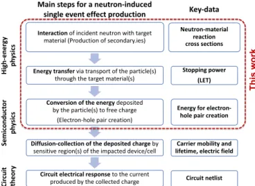
eight materials: GaAs, AlAs, InP, InAs, GaSb, InSb, GaN and GaP. For each material, we investigated the first steps of the production of atmospheric neutron-induced single event effects, as illustrated in Fig. 1. These single particle effects are the consequences of interactions of neutrons, created in atmospheric cascading showers, with a target of bulk material exposed at ground level to this natural flux of neutrons. Neutron interactions result in the production of secondary charged particles that deposit their energy in the material and create electron-hole pairs along their path [12]. As we will show in the following, quantitative data extracted from these first steps give important indications on the susceptibility of such materials to natural radiation at ground level, by considering the case of bulk silicon as the reference material for systematic comparison purpose.
Fig. 1. Synopsis of the production of neutron-induced single event effects showing the first steps investigated in this work. LET means linear energy transfer.
The paper is organized as follows. Section II presents the different compound materials studied and summarizes their main physical and electronic properties. Section III details the direct and Geant4 calculation of the atmospheric neutron reaction rate in a layer of material. Section IV presents a complete analysis of neutron-induced secondaries produced in these III-V materials using Geant4 [13-14]. Finally, in section V, implications for single event effects are discussed in terms of electrical charge deposited in the material with respect to the critical charge for technologies ranging from 180nm to 14nm.
Interaction of incident neutron with target material (Production of secondary.ies)
Energy transfer via transport of the particle(s) through the target material(s) Conversion of the energy deposited
by the particle(s) to free charge (Electron-hole pair creation) Diffusion-collection of the deposited charge by
sensitive region(s) of the impacted device/cell Circuit electrical response to the current
produced by the collected charge
Hi gh -en er gy ph ys ic s Se mi co nd uc to r ph ys ic s Ci rcu it th eo ry Neutron-material reaction cross sections Stopping power (LET) Energy for
electron-hole pair creation Carrier mobility and lifetime, electric field
Circuit netlist Main steps for a neutron-induced
single event effect production Key-data
Thi
s
w
or
k
Atmospheric Neutron Radiation Response
of III-V Binary Compound Semiconductors
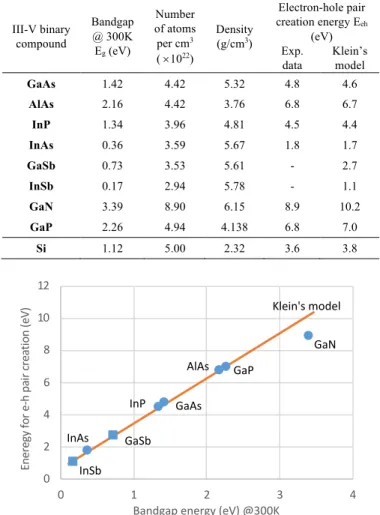
The III-V binary compounds studied in the following are made from seven chemical elements from columns III (Al, Ga, In) and V (N, P, As, Sb) of the periodic table. We voluntary excluded boron-based compounds (BN, BP, BAs, BSb) from this study, due to the thermal neutron sensitivity of these materials (if not selective in isotopes) induced by the presence of 10B [15-17]. Eight compound materials have thus been considered: GaAs, AlAs, InP, InAs, GaSb, InSb, GaN and GaP (GaAs and GaN materials have been recently explored in [18]). Table I summarizes the main experimental values for these materials in terms of bandgap, density, and electron-hole pair creation energy. Due to their composition and crystallographic structure, all these materials are more dense than Si (2.32 g/cm3); five materials (GaAs, AlAs, InP, GaN, GaP) exhibit a bandgap larger than Si and logically a larger electron-hole pair creation energy (3.6 eV for Si), three materials (InAs, GaSb, InSb) are low bandgap semiconductors (< 1eV) with lower electron-hole pair creation energy than Si. The value of electron-hole pair creation energy Eeh is currently missing in literature for GaSb and InSb; we used values deduced from the Klein’s model [19] linking energy bandgap and energy for e-h pair creation in semiconductor materials (Fig. 2).
TABLE I.MAIN PROPERTIES OF THE III-V BINARY COMPOUNDS STUDIED IN THIS WORK.VALUES FOR SI ARE ALSO REPORTED.
III-V binary compound Bandgap @ 300K Eg (eV) Number of atoms per cm3 ( ´1022) Density (g/cm3) Electron-hole pair creation energy Eeh (eV) Exp. data Klein’s model GaAs 1.42 4.42 5.32 4.8 4.6 AlAs 2.16 4.42 3.76 6.8 6.7 InP 1.34 3.96 4.81 4.5 4.4 InAs 0.36 3.59 5.67 1.8 1.7 GaSb 0.73 3.53 5.61 - 2.7 InSb 0.17 2.94 5.78 - 1.1 GaN 3.39 8.90 6.15 8.9 10.2 GaP 2.26 4.94 4.138 6.8 7.0 Si 1.12 5.00 2.32 3.6 3.8
Fig. 2. Energy for e-h pair creation as a function of the bandgap energy for the III-V binary compound materials studied in this work.
SECTION IN EDNFB-VII.1 AND TENDL-2017 NUCLEAR DATA LIBRARIES.
Symbol number Atomic Nuclide abundance Natural
ENDFB-VII.1. (20 MeV) TENDL-2017 (200 MeV) Al 13 13-Al-27 100.00% ✓* ✓ Ga 31 31-Ga-69 60.10% ✓ ✓ 31-Ga-71 39.90% ✓ ✓ In 49 49-In-115 95.70% ✓ ✓ 49-In-113 4.30% ✓ ✓ N 7 7-N-14 99.60% ✓ * ✓ 7-N-15 0.40% ✓ ✓ P 15 15-P-31 100.00% ✓* ✓ As 33 33-As-75 100.00% ✓ ✓ Sb 51 51-Sb-121 57.40% ✓ ✓ 51-Sb-123 42.60% ✓ ✓ Si 14 14-Si-28 92.20% ✓* ✓ 14-Si-29 4.70% ✓* ✓ 14-Si-30 3.10% ✓* ✓ *Extended to 120 MeV
Fig. 3. High energy (> 1 MeV) neutron (total) cross sections for the main nuclides related to the III-V materials studied. Data from the TENDL-2017 nuclear data library.
Table II indicates the isotope composition of the elements related to the III-V compounds studied in this work and their natural abundance. The study of atmospheric neutron interactions with the compounds of Table I requires: i) the availability of neutron cross-sections for all nuclides listed in Table II and ii) if possible, an extended energy range above 1 MeV, due to the nature of the atmospheric neutron spectrum [20]. Even if the US standard evaluated nuclear data library ENDF/B (ENDFB-VII.1) [21] responds well to the first point (in particular for In and Sb that are not included in all nuclear data libraries), however, the upper energy limit is only 20 MeV for Ga, In, Sb and As. After checking of several nuclear data libraries, we choose the new release of the TENDL library (TENDL-2017) [22] that offers availability of all neutron cross-sections up to 200 MeV. Fig. 3 shows the total cross cross-sections
0 2 4 6 8 10 12 0 1 2 3 4 En er egy fo r e -h pa ir cr ea tion (e V)
Bandgap energy (eV) @300K
GaN GaP AlAs GaAs InP GaSb InAs InSb Klein's model
for the most abundant nuclides for the seven elements and also for 14-Si-28 for comparison. These data are used in the next section to evaluate the neutron reaction rate in a layer of the different compound materials.
III. NEUTRON REACTION RATES IN A LAYER OF MATERIAL
The susceptibility of the studied materials to atmospheric neutron has been roughly evaluated by a direct calculation of the reaction rate in a target representative of a microelectronic circuit, following a method introduced by Wrobel et al [23].
According to [23], we first calculated the number of nuclear reactions Rn in a material layer with an area of S=1 mm2, a thickness of e=1 µm and an atomic density equal to that of silicon (N=5 ´1022 at./cm3). Rn is simply given by:
𝑅!= 𝑁𝑒 ∫$%(!$%&'𝜎(𝐸)"#"$𝑑𝐸 (1)
where s(E) is the neutron cross section of the considered element constituting the material, dj/dE is the differential neutron flux, Emin and Emax are the limits of the energy domain considered (in the following, Emin = 1 MeV and Emax = 200 MeV).
To evaluate Eq. (1), we considered in our calculation the differential neutron flux shown in Fig. 4 measured by Goldhagen et al. [24] and modeled by Gordon et al. [20] under the form of an analytical fitting function given by:
"# "$= 𝐴 × 𝑒𝑥𝑝[𝐵(𝑙𝑛𝐸) )+ 𝐶𝑙𝑛(𝐸)] + 𝐷 × 𝑒𝑥𝑝[𝐹(𝑙𝑛𝐸))+ 𝐺𝑙𝑛(𝐸)] + (2) with A = 1.006´10-6, B = -0.35, C = 2.1451, D = 1.011´10-3, F = -0.4106 and G = -0.667.
Fig. 4. Differential atmospheric neutron flux as a function of neutron energy measured by Goldhagen et al. [24] and modeled by Gordon et al. [20] in the energy range above 1 MeV and under reference conditions (sea level, New York City, mid-level solar activity, outdoors).
Fig. 5 shows the results of our calculations using Eq. (1) applied to “materials” constituted by a single element of Table II with an isotope composition mimicking the natural abundance. In order to compare with Wrobel’s data, nuclear rates are expressed for a duration of 109 h and for a neutron flux corresponding to 12 km altitude. Our results shown in Fig. 5 are in very good agreement with Wrobel’s data. For each element, we give in addition the number of elastic and nonelastic events
Fig. 5. Calculated number of nuclear interactions in 109 h induced by high
energy (>1 MeV) atmospheric neutrons in a layer of material of 1 mm2. Data
are compared to previous results published in [16].
Fig. 6. Calculated number of nuclear interactions induced by atmospheric neutrons in different III-V binary compound materials (exact composition with natural abundance of nuclides) deduced from Eq. (1) for ENDFB-VII.1 and TENDL-2017 nuclear data libraries and from Monte Carlo simulations using Geant4.
(see definitions in IV.A) directly evaluated from TENDL-2017 (MF=3, MT=2 for elastic cross section). From data of Fig. 5, the reaction rates for all the III-V materials of Table I can be deduced, taken into account the exact number of atoms per cm3 and the binary nature of the compounds. In order to compare with our previously published results on Si [25], Ge and SiC [18], we change in the following the normalization factors introduced for the expression of the nuclear rates, choosing now: S = 1 cm2, e = 20 µm, duration of 5x10⁶ h and neutron flux at sea level. With respect to Wrobel’s conditions previously used in Fig. 5, these differences result in new reaction rates equal to Wrobel’s ones exactly divided by a numerical factor of 50.
Fig. 6 shows the results of these calculations for nuclear interaction rates evaluated from ENDFB-VII.1 and TENDL-2017 nuclear data libraries and from Monte Carlo simulations using Geant4 version 4.9.4 patch 01 (eight separate runs for each compound as the target material). The list of physical processes employed in these simulations is based on the standard package of physics lists QGSP_BIC_HP [26]. Details are given in Appendix A. Other simulation details can be found in Ref. [18]. N AlSi P Ga As In Sb 0 5000 10000 15000 20000 25000 30000
GaAs AlAs InP InAs GaSb InSb GaN GaP Silicon
N umb er o f i nte racti on s
Atmospheric neutron interactions (1cm2x 20 µm, 5x10⁶h @ sea level)
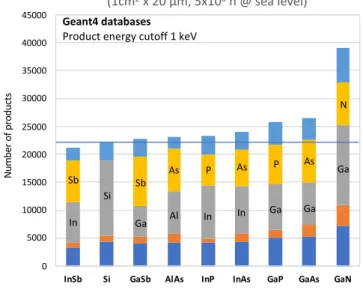
the exact number of atoms per volume unit leads to significantly narrow the range of values: almost all materials, GaN excepted, exhibit similar global reaction rates, between 15,000 and 20,000 (Geant4 values) for the 1 cm2x 20 µm target exposed during 5´106 h. These values respectively correspond to interaction rates equal to 7.5´105 and 1´106 for 1mm2 ´ 1µm target exposed during 109 h. Geant4 values are logically found greater to those derived from ENDFB-VII.1 (limited to 20 MeV in energy) and in good agreement with those obtained with TENDL-2017. In the next section, Geant4 databases are analyzed in order to examine in detail the production of secondaries for the different binary compounds.
IV. DETAILED ANALYSIS OF INTERACTIONS AND SECONDARIES A. Geant4 database analysis
Geant4 databases have been computed for the eight III-V compound materials and for Si exactly with the same compilation rules: i) the Geant4 code eliminates in the output file (raw data) all secondaries below 1 keV of energy; ii) a post-treatment script compiles the final database from raw data by eliminating all g photons, p0, e+, e- and h particles, not able to induce significant single event effects in such materials. The energy cutoff of 1 keV corresponds, for each material, to an amount of deposited electrical charge equal to 1 keV/Eeh (Eeh given Table I) well below the minimal critical charge of the current and future technologies (see paragraph IV.B). Its value is thus sufficiently low to guarantee that all products susceptible to play a significant role at electronic circuit level and for all materials are taking into account in our analysis.
Fig. 7 shows the distributions of elastic, inelastic and nonelastic events for the different III-V compound materials and for Si, as obtained from the analysis of the computed databases with the energy cutoff of 1 keV previously defined. For memory, interactions of neutrons with atomic nuclei can be divided in two major mechanisms: scattering (elastic, inelastic) and capture (or non-elastic) [27-28]. In the elastic scattering, the nature of the interacting particles is not modified; the recoil nucleus is then the same as the target nuclei A or B in the case of a binary compound material AB. The inelastic scattering is similar to the elastic scattering except that the impacted target nucleus A or B undergoes an internal rearrangement into an excited state from which it eventually releases radiation. Instead of being scattered, an incident neutron may be absorbed or captured by a target material nucleus A or B. Many reactions are possible and a large variety of particles can be emitted. This type of interaction is also called nonelastic interaction.
In Fig. 7, materials have been ordered according to the increasing number of interactions: all III-V materials exhibit a higher interaction rate than the one of Si. Between all materials, GaSb, AlAs and InSb show the number of interaction events the closest from the one of Si. GaN show the highest number of interactions, mainly due to the number of atoms per volume unit for this compound semiconductor which is almost double with respect to all other materials (see Table I).
The proportion of elastic events is clearly predominant for Si
inelastic+nonelastic events are the majority products for GaAs (56%), InAs, InSb (54%) and GaSb (53%). For Si, inelastic+nonelastic events are around 32%, which is lower than 40% found in previous studies [25]. But we have to remember that, in the present case, all recoils and secondaries with energies as low as 1 keV were taken into account in the databases, contrary to the case of previous studies for which a cutoff energy of 40 keV was used. As we will see in the next paragraph (IV.B), such proportions of elastic and inelastic+ nonelastic events depend of the product energy cutoff fixed to conserve or reject products as soon as they are pertinent or not to induce SEEs with respect to a given technological node. It is the reason why these percentages may vary.
Fig. 7. Number of elastic, inelastic and nonelastic interactions induced by atmospheric neutrons in the different III-V binary compound materials obtained from Geant4 simulations.
Fig. 8. Distribution of products resulting from the interactions of atmospheric neutrons with the different III-V binary compound materials obtained from Geant4 simulations.The horizontal line corresponds to the total in the case of silicon for eye guide.
11369 7868 9246 8210 9636 8432 8426 10556 15587 2048 6624 4490 6146 5392 6642 6374 4524 6349 3373 2574 3508 3298 3218 3290 4356 4150 6537 0 5 000 10 000 15 000 20 000 25 000 30 000
Si InSb AlAs GaSb InP InAs GaAs GaP GaN
N umb er o f i nte racti on s
Atmospheric neutron interactions (1cm2x 20 µm, 5x10⁶h @ sea level)
Elastic Inelastic Nonelastic
Geant4 databases
Product energy cutoff 1 keV
0 5000 10000 15000 20000 25000 30000 35000 40000 45000
InSb Si GaSb AlAs InP InAs GaP GaAs GaN
Nu m be r o f p ro du ct s
Secondaries produced in all interactions
(1cm2x 20 µm, 5x10⁶h @ sea level)
protons, deuterons, tritons alphas, He-3 Recoils #1 Recoils #2 Others Ga As Al As In P In In Sb Sb As Ga Ga N P Ga Si Geant4 databases
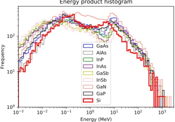
Fig. 8 shows the distribution of all secondaries produced in these interactions between atmospheric neutrons and the different targets of III-V binary compound materials; Fig. 9 gives their energy distribution. Four groups of particles have been defined in Fig. 8: i) protons, deuterons and tritons (Z=1), ii) alpha particles and He-3 (Z=2), iii) nuclei corresponding to target atoms (named recoils #1 and #2 for binary compounds) and iv) other nuclei. Similar distributions of these particle groups are found for all materials, GaN excepted, with approximately 20-25% of protons+alphas, 60% of target nuclei and the remaining 15% of other nuclei. For GaN, a higher proportion of protons and alpha particles is observed (more than two times the quantity observed in Si), due to significant cross sections for 14N(n,p)14C and 14N(n,a)11B reactions. For this material, the combined effects of a high density and the presence of nitrogen leads to such a large difference with respect to other III-V materials in terms of a higher number of interactions, of secondaries produced and of alphas and protons. Histograms of Fig. 9 show that, with respect to Si, interactions in III-V compound materials generate more low energy products (typically below 0.1 MeV) and more high energy products (above 10 MeV). On contrary, in the energy domain between 0.1 MeV and 10 MeV, more products are observed for Si with respect to the other materials, except for GaN which exhibits the largest distribution above 0.1 MeV.
Such energy product distributions can be explained by resolving the respective distributions of protons, alpha particles, target nucleus recoils and other ions, shown in Fig. 10 for GaN and InSb (the two extreme cases evidenced in Fig. 9) and also for the reference Si. Below 0.1 MeV, the greater number of recoils for InSb and GaN than for Si is the direct consequence of higher elastic cross sections for these higher-Z atoms (Ga, In, Sb) than those for Si and of a higher number of atoms per volume unit for GaN. Around and above 1 MeV, important difference in alpha and proton distributions (total numbers and positions of the maxima) for these three materials explain the respective positions of the distributions observed in Fig. 9. In particular, alpha particles are found to be produced with higher energies (up to 100 MeV) in all III-V materials than in Si (maximum 35 MeV), due to the nature of nuclear reaction channels for such higher-Z atoms.
Fig. 9. Energy histograms (100 bins) of all secondary products induced by atmospheric neutron interactions in the different III-V material targets (also including silicon for comparison).
Fig. 10. Energy histograms (100 bins) of protons, alphas, target nucleus recoils and other ions produced by atmospheric neutron interactions in Si, InSb and GaN targets.
B. Low energy threshold versus technological nodes
In previous studies and for standardization purposes [18,25], we systematically eliminated for the database analysis all secondary particles not able to deposit an electrical charge in the target material above a certain threshold quantity, arbitrary fixed to 1.8 fC [25]. This criterion mechanically decreased the number of less energetic events and potentially eliminates secondary products that may induce significant SEEs in the most integrated technologies. In this paragraph, we would like to evaluate the impact of such a criterion on the database analysis and to extend the range-of-interest of our results to more integrated technological nodes (initially, 1.8fC has been chosen as it corresponded in 2010 to the typical critical charge of a bulk silicon 65nm SRAM technology).
For this purpose, we consider the current values of the minimum critical charge for standard SRAM memory cells as a function of the technological node, as given by Table III (after Seifert et al. [29]). For each semiconductor material, this value is converted into a threshold energy (that corresponds to the energy necessary to create the critical charge when totally absorbed and converted into e-h pairs) considering the value of the electron-hole pair creation energy Eeh given in Table I. For example, a critical charge of 0.9 fC (that corresponds to the 45nm node) corresponds to a threshold energy value of 20.2 keV in the case of silicon and to 50 keV in the case of GaN, etc. Doing this for each node and each material, we applied a post-treatment script on the computed Geant4 databases to eliminate all interactions giving secondary products with energies below this threshold. Results of these processing are shown in Fig. 11. The number of interactions dramatically decreases for all materials, primarily eliminating the less energetic elastic events and, to a lesser extent, the number of inelastic events.
Fig. 12. Percentage of elastic interactions in the total number of atmospheric neutron-material target interactions of Fig. 7 as a function of technological node for the different III-V compounds and for the reference Si. The decrease of the critical charge versus technology integration requires to take into account more and more low energy elastic events susceptible to induce SEEs when decreasing from 180 nm to 14 nm nodes.
TABLE III.MINIMUM CRITICAL CHARGE VERSUS TECHNOLOGICAL NODES FOR STANDARD SRAM MEMORY CELLS.AFTER [29].
Technological
node (nm) 180 130 90 65 45 32 22 14
Critical charge
Qcrit (fC) 3.5 2.9 1.9 1.3 0.9 0.85 0.8 0.7
Fig. 11. Remaining number of interactions in III-V and Si material targets giving secondary products above a certain energy threshold calculating from the critical charges of Table III for technological nodes ranging from 180 nm to 14 nm. 1 keV data correspond to the number of interactions contained in Geant4 databases before event rejection considering this energy threshold per node.
These decreases are, logically, the most important for the 180 nm (characterized by the highest critical charge of 3.5 fC) and reaches minimum values for the 14 nm node (minimum critical charge of 0.7 fC) for which more elastic events produce recoils with energies above the threshold limit. Note that, in the same time, the number of nonelastic events are not impacted by this filtering criterion because all the threshold values are well below the energies of produced secondaries, typically in the order of a few MeV.
The decrease of the critical charge versus technology integration thus requires considering more and more low energy elastic events susceptible to induce SEEs when decreasing from 180 nm to 14 nm nodes. The continuous lines in Fig. 11 graphically represents these two extreme cases for all studied materials: the passage from 180 nm to 14nm requires to take
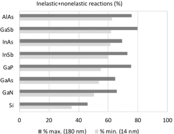
into account +36% of interactions in the case of Si, +40% for InAs, +52% for InSb, +56% for InP, +57% for GaN, +61% for GaSb, +66% for GaAs, +75% for GaP and finally +77% for AlAs. In case of numerical simulations of SEEs in a given technology, this should represent a nonnegligible numerical cost to properly take into account all low energy interaction events in the simulation flow. The direct consequence of such increases of the number of pertinent interaction events with technology downscaling is the evolution of the percentages, on one hand of elastic interactions, and on the other hand, of (inelastic+nonelastic) reactions in the global number of interactions. This is illustrated in Figs 12 and 13. Fig. 12 quantifies the increase with downscaling of the percentage of elastic interactions for the different target materials and Fig. 13 gives the percentage of inelastic+noneleastic reactions for the two extreme cases corresponding to 180 nm and 14 nm nodes. In Fig. 13, we can see that for silicon, the value of 40% of inelastic+nonelastic events commonly reported in literature [25] correspond in fact to a median value for current technologies, but this proportion varies from 45% to 35% when downscaling technologies from 180 to 14 nm.
Fig. 13. Percentage of inelastic+nonelastic interactions in the total number of interactions per material defined in Fig. 7 for the limit cases corresponding to technological nodes 180 nm and 14 nm.
0 10 20 30 40 50 60 70 80
Si GaAs AlAs GaP GaSb InAs InP GaN InSb
P er ce nt ag e of e la st ic in te ra ct io ns (% ) 180 nm 130 nm 90 nm 65 nm 45 nm 32 nm 22 nm 14 nm 1 keV 7000 10000 13000 16000 19000 22000 25000 28000
InP GaSb GaP AlAs GaAs InSb Si InAs GaN
N um be r of in te ra ct io ns
Atmospheric neutron interactions (1cm2x 20 µm, 5x10⁶h @ sea level) 180 nm 130 nm 90 nm 65 nm 45 nm 32 nm 22 nm 14 nm 1 keV Geant4 databases 0 20 40 60 80 100 Si GaN GaAs GaP InSb InAs GaSb AlAs Inelastic+nonelastic reactions (%) % max. (180 nm) % min. (14 nm)
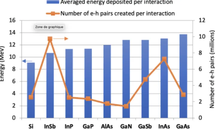
Fig. 14. Averaged values of the deposited energy per interaction and corresponding amounts of created e-h pairs for the different III-V material and Si targets. Values have been evaluated considering for each material the e-h pair creation energy given in Table I.
Fig. 13 also shows that, for all III-V materials, the percentage of inelastic+nonelastic events is clearly higher that for Si, well above 50% in all cases and above 60% for GaSb, AlAs, InAs and InSb; it is extremely high for GaSb and reaches the value of 80% when low energy elastic events are not considered (180 nm node).
V. IMPLICATIONS FOR THE SEES
The conversion of the deposited energy into electrical free charge, via the formation of electron-hole pairs, is also an essential mechanism in the creation of single event effects (see Fig. 1). In the present approach that is limited to only provide a global view from the analysis of interaction databases, two interesting metrics can be evaluated: i) the averaged value of deposited energy per interaction and ii) the corresponding amount of created e-h pairs. These two metrics have been calculated, in Fig. 14, for all materials. The averaged deposited energy per interaction is found to vary from approximatively 9 MeV for Si to 14 MeV for GaAs. Atmospheric neutron interactions deposit, in average, more energy in III-V materials than in Si. This result is certainly due to the higher number of nonelastic interactions in the III-V materials than in Si.
Concerning the number of e-h pairs created per interaction, we compare this number of pairs with respect to the value obtained for silicon (relative factor). Three groups of materials can be distinguished in Fig. 14: 1) GaAs, AlAs, InP, GaN and GaP that are finally found very similar to Si (relative factor close to 1 with respect to Si); 2) InAs and GaSb which exhibit a relative factor between 1.5 and 2.5 and, finally, 3) InSb characterized by the highest factor, close to 4. For the first group of materials, everything happens as if the higher atmospheric neutron sensitivity of these materials in terms of number of interactions is counterbalanced by a higher e-h pair creation energy at semiconductor level, due to their large bandgap. On the contrary, for the three last materials that correspond to the lower bandgap semiconductors (see Table I), their susceptibility to atmospheric neutrons is finally more important at material electrical response level due to the relatively low values of the e-h pair creation energy.
This preliminary exploration of III-V binary compound
materials should be now completed by the evaluation of the impact of carrier mobilities and lifetimes on the formation of single-event transients at device level (typically in reversely biased junctions) to more quantitatively conclude at electrical level on their level of vulnerability to natural neutron radiation at ground level.
VI. CONCLUSION
In this work, we explored by simulation the radiation response of III-V binary compound semiconductors subjected to high energy atmospheric neutrons. Eight III-V materials have been considered: GaAs, AlAs, InP, InAs, GaSb, InSb, GaN and GaP. The susceptibility of these materials to atmospheric neutron has been firstly evaluated by a direct calculation of the interaction rates from neutron cross-sections in a target representative of a circuit. We showed that all materials, GaN excepted, exhibit similar global reaction rates, between 7.5´105 and 1´106 for 1mm2 ´ 1µm target exposed during 109 h to atmospheric neutrons. GaN is distinguished by a much higher rate of events, of the order of ´2 with respect to Si, than can be relied to a similar factor in the number of atoms per volume unit for this very dense material. From the exploitation of Geant4 databases computed for the eight III-V compound materials and for Si, we carefully analyzed the distributions of events and of secondary products, highlighting significant differences in the atmospheric neutron radiation response of such materials in terms of elastic, inelastic and nonelastic interaction rates, and also in terms of respective weights of protons, alphas and recoils in the production of secondaries. Database analysis has been then conducted by introducing an energy cutoff related to the typical value of the critical charge for technology nodes ranging from 180 to 14 nm. We showed that the decrease of the critical charge versus technology integration requires to take into account more and more low energy elastic events susceptible to induce single event effects. This aspect has been quantified, showing its importance for all III-V materials. Finally, the conversion of the deposited energy into electrical free charge allowed us to quantify the averaged values of the deposited energy per interaction and the corresponding amounts of created e-h pairs for the different III-V material and Si targets. The results suggest that the atmospheric neutron sensitivity of large band-gap materials (GaAs, AlAs, InP, GaN and GaP), evidenced by the numbers of interactions and secondary products, is largely counterbalanced by a higher e-h pair creation energy at semiconductor level that leads to amounts of free charge comparable to the one of silicon. On the contrary for low bandgap semiconductors (InAs, GaSb, InSb), their susceptibility is amplified due to the relatively low values for e-h pair creation energies that lead to larger amounts of free charges with respect to Si. This preliminary exploration of III-V binary compound materials will have to be continued to evaluate the next steps of creation of single events effects in such materials related to the formation of current transients at device levels, in order to study the impact of transport and carrier properties on the atmospheric radiation response of III-V material-based electronics.
The list of physical processes employed in the reported Geant4 simulations is based on the standard package of physics lists QGSP_BIC_HP [26]. Concerning the hadronic interactions, in QGSP group of physics lists the quark gluon string model is applied for high-energy (above ~12 GeV) interactions of protons, neutrons, pions, kaons and nuclei. The high-energy interaction creates an excited nucleus, which is passed to the precompound model describing the nuclear de-excitation. Nuclear capture of negative particles is simulated within the Chiral Invariant Phase Space (CHIPS) model. QGSP_BIC_HP list includes binary cascade for primary protons and neutrons with energies below ~10 GeV, and also uses binary light ion cascade for inelastic interaction of ions up to few GeV/nucleon with matter. The complete list of the Geant4 classes that we considered for our neutron simulations is summarized in Table IV below.
TABLE IV.LIST OF THE DIFFERENT GEANT4 CLASSES CONSIDERED IN THE PRESENT SIMULATION FLOW FOR THE DESCRIPTION OF NEUTRON-MATTER INTERACTIONS.
Neutron
process Energy Geant4 model Dataset
Elastic < 20 MeV > 20 MeV G4NeutronHPElastic G4LElastic G4NeutronHP ElasticData Inelastic < 20 MeV [20 MeV, 10 GeV] G4NeutronHPInelastic G4BinaryCascade G4LENeutronInelastic QGSP G4NeutronHPI nelasticData
Fission < 20 MeV > 20 MeV G4NeutronHPFission G4LFission G4NeutronHPFissionData Capture < 20 MeV > 20 MeV G4NeutronHPCapture G4LCapture G4NeutronHPCaptureData
VIII. REFERENCES
[1] H. Riel, L. Wernersson, M. Hong, J. Del Alamo, “III–V compound semiconductor transistors—from planar to nanowire structures”, MRS Bulletin, 39(8), 668-677, 2014.
[2] S. Oktyabrsky, P. Ye, Fundamentals of III-V Semiconductor MOSFETs, Springer Science & Business Media, 2010.
[3] T. Li, M. Mastro, A. Dadgar, III–V Compound Semiconductors: Integration with Silicon-Based Microelectronics, CRC Press, 2016. [4] A.A. Jönsson, J. Svensson and L. Wernersson, “A Self-Aligned Gate-Last Process Applied to All-III–V CMOS on Si,” IEEE Electron Device Letters, vol. 39, no. 7, pp. 935-938, July 2018. [5] K. Ni et al., “Single-Event Transient Response of InGaAs
MOSFETs,” in IEEE Transactions on Nuclear Science, vol. 61, no. 6, pp. 3550-3556, Dec. 2014.
[6] H. Gong et al., “Scaling Effects on Single-Event Transients in InGaAs FinFETs,” in IEEE Transactions on Nuclear Science, vol. 65, no. 1, pp. 296-303, Jan. 2018.
[7] H. Gong et al., “Pulsed-Laser Induced Single-Event Transients in InGaAs FinFETs on Bulk Silicon Substrates,” IEEE Transactions on Nuclear Science, vol. 66, no. 1, pp. 376-383, Jan. 2019. [8] C.H. Tsao, R. Silberberg and J.R. Letaw, “A comparison of
neutron-induced SEU rates in Si and GaAs devices,” IEEE Transactions on Nuclear Science, vol. 35, no. 6, pp. 1634-1637, Dec. 1988.
[10] D. McMorrow, J.S. Melinger, A.R. Knudson, “Single-event effects in III-V semiconductor electronics”, International Journal of High-Speed Electronics and Systems Vol. 14, No. 2, 311-325, 2004. [11] H. Liu, M. Cotter, S. Datta, V. Narayanan, vTechnology Assessment
of Si and III-V FinFETs and III-V Tunnel FETs from Soft Error Rate Perspective”, International Electron Device Meeting, Institute of Electrical and Electronics Engineers, 2012, pp. 577-580.
[12] D. Munteanu, J.L. Autran, “Modeling and simulation of single-event effects in digital devices and ICs”, IEEE Transactions on Nuclear Science vol. 55, no. 4, pp.1854-1878, 2008.
[13] S. Agostinelli et al., “Geant4 – a simulation toolkit”, Nuclear Instruments and Methods in Physics Research Section A: Accelerators, Spectrometers, Detectors and Associated Equipment, vol. 506, no. 3, pp. 250-303, 2003.
[14] J. Allison, K. Amako, J. Apostolakis, P. Arce, M. Asai et al., “Recent developments in Geant4”, Nuclear Instruments and Methods in Physics Research Section A: Accelerators, Spectrometers, Detectors and Associated Equipment, vol. 835, pp. 186-225, 2016.
[15] J.F. Ziegler, H. Puchner, SER – History, Trends and Challenges, Cypress Semiconductor, 2004.
[16] R. Baumann, T. Hossain, S. Murata, H. Kitagawa, “Boron Compounds as a Dominant Source of Alpha Particles in Semiconductor Devices,” IEEE International Reliability Physics Physics Symposium, 1995, pp. 297-302.
[17] J.L. Autran, S. Serre, S. Semikh, D. Munteanu, G. Gasiot, P. Roche, “Soft-Error Rate Induced by Thermal and Low Energy Neutrons in 40 nm SRAMs”, IEEE Transactions on Nuclear Science, vol. 59, no. 6, pp. 2658-2665, 2012.
[18] D. Munteanu D and J.L. Autran, “Susceptibility of Group-IV and III-V Semiconductor-based Electronics to Atmospheric Neutrons Explored by Geant4 Numerical Simulations”. In: S. Rao (Ed.) Numerical Simulations, Intech, Vienna, pp. 117-134, 2018. [19] C.A. Klein, “Bandgap Dependence and Related Features of
Radiation Ionization Energies in Semiconductors”, Journal of Applied Physics. 39. 2029 – 2038, 1968.
[20] M.S. Gordon et al., “Measurement of the Flux and Energy Spectrum of Cosmic-Ray Induced Neutrons on the Ground,” IEEE Transactions on Nuclear Science, vol. 51, pp. 3427-3434, 2004. [21] M.B. Chadwick et al. “ENDF/B-VII.1 Nuclear Data for Science and
Technology: Cross Sections, Covariances, Fission Product Yields and Decay Data,” Nuclear Data Sheets, vol. 112, pp. 2887-2996, 2011.
[22] D. Rochman, A.J. Koning, J.Ch. Sublet, M. Fleming, et al., "The TENDL library: hope, reality and future", proceedings of the International Conference on Nuclear Data for Science and Technology, September 11-16, 2016, Bruges, Belgium.
[23] F. Wrobel, J. Gasiot, F. Saigné, and A.D. Touboul, “Effects of atmospheric neutrons and natural contamination on advanced microelectronic memories”, Appl. Phys. Lett. 93, 064105, 2008. [24] P. Goldhagen, “Cosmic-Ray Neutrons on the Ground and in the
Atmosphere”, MRS Bulletin, vol. 28, no. 2, pp. 131-135, 2003. [25] S. Serre, S. Semikh, S. Uznanski, J.L. Autran, D. Munteanu, G.
Gasiot, P. Roche, “Geant4 Analysis of n-Si Nuclear Reactions From Different Sources of Neutrons and Its Implication on Soft-Error Rate”, IEEE Transactions on Nuclear Science, vol. 59, no. 4, pp. 714-722, 2012.
[26] Geant4 version 4.9.4. Online available:
http://geant4.cern.ch/collaboration/working_groups/electromagneti c/physlist9.4.shtml
[27] J.L. Autran, D. Munteanu, Soft Errors: from particles to circuits. Taylor & Francis/CRC Press, 2015.
[28] P. Rinard, “Neutron Interactions with Matter”, Los Alamos Technical Report (1991).
[29] N. Seifert, S. Jahinuzzaman, J. Velamala, R. Ascazubi, N. Patel, B. Gill, J. Basile, J. Hicks, “Soft Error Rate Improvements in 14-nm Technology Featuring Second-Generation 3D Tri-Gate Transistors”, IEEE Transactions on Nuclear Science, vol. 62, no. 6, pp. 2570-2577, 2012.