HAL Id: hal-02448461
https://hal.archives-ouvertes.fr/hal-02448461
Submitted on 5 Jan 2021
HAL is a multi-disciplinary open access
archive for the deposit and dissemination of
sci-entific research documents, whether they are
pub-lished or not. The documents may come from
teaching and research institutions in France or
abroad, or from public or private research centers.
L’archive ouverte pluridisciplinaire HAL, est
destinée au dépôt et à la diffusion de documents
scientifiques de niveau recherche, publiés ou non,
émanant des établissements d’enseignement et de
recherche français ou étrangers, des laboratoires
publics ou privés.
Atomic force microscopy developments for probing space
charge at sub-micrometer scale in thin dielectric films
Christina Villeneuve-Faure, Laurent Boudou, K Makasheva, G. Teyssedre
To cite this version:
Christina Villeneuve-Faure, Laurent Boudou, K Makasheva, G. Teyssedre. Atomic force microscopy
developments for probing space charge at sub-micrometer scale in thin dielectric films. IEEE
Transac-tions on Dielectrics and Electrical Insulation, Institute of Electrical and Electronics Engineers, 2016,
23 (2), pp.713-720. �10.1109/TDEI.2016.005319�. �hal-02448461�
1
Atomic Force Microscopy developments for probing space
charge at sub-micrometer scale in thin dielectric films
C. Villeneuve-Faure, L. Boudou, K. Makasheva and G. Teyssedre
LAPLACE (Laboratoire Plasma et Conversion d’Energie), Université de Toulouse; UPS, INPT, CNRS; 118 route de Narbonne, F-31062 Toulouse cedex 9, France
ABSTRACT
Charge injection and accumulation in dielectrics are phenomena at the origin of different kind of failure of devices. To improve the understanding of involved mechanisms, space charge measurement techniques have been successfully developed. However, their spatial resolution is incompatible with thin films or interfaces studies. In this paper, the contribution of techniques derived from Atomic Force Microscopy (AFM) to space charge measurement is investigated. First of all, localized charges injection is studied using classical Kelvin Force Microscopy (KFM). Secondly, we propose a new method called EFDC (Electrostatic Force Distance Curve) which allows direct measurement of electrostatic force induced by trapped charges. EFDC sensitivity to lateral localization of charges is demonstrated. Finally, comparing the results obtained by EFDC and KFM highlights the relative merit of each technique.
Index Terms — Atomic Force Microscopy, Dielectric materials, Space charge, Kelvin Force Microscopy, Electrostatic force
1
INTRODUCTION
Physical dimension of solid dielectrics, involved in industrial applications, range from few centimeters (electrotechnics) to few tens of nanometers (electrets or microsystems). Whatever their main scale, most insulating materials accumulate electrical charges under applied electric field. This phenomenon is useful for some applications as electrets or nonvolatile memories [1] but in many other instances it leads to a failure [2]. Consequently, performing space charge measurements is needed to predict and to analyze these charging effects.
Conventional space charge measurements are based on acoustic or thermal perturbation whose shape influences strongly the ultimate resolution [3-4]. Acoustic perturbation as implemented in Pulsed ElectroAcoustic (PEA) technique [5] provides up to 3-4µm of in-depth resolution but without lateral resolution. Concerning thermal perturbation, thermal pulse (TP) and Laser Induced Modulation Method (LIMM) manage to reach 1µm of in-depth resolution [6], but without lateral resolution. The development of Focused LIMM (FLIMM) has brought lateral resolution of the order of 5µm [7]. With recent developments, the actual resolution is improved and now limited mainly by instrumental point of view (perturbation shape, attenuation/dispersion for acoustic waves, deconvolution procedure [6]…) Table 1 summarizes the resolution reached and the expected one for thermal and
acoustic methods. Though some improvements have been achieved, up to now such techniques are unsuitable for characterizing the charge accumulation in thin films (a few 100 nm thickness) for microelectronics and microsystems applications or for studies of phenomena occurring at metal / dielectric or semiconductor / dielectric interfaces. Therefore, two ways appear to improve resolution: to push the instrumental limits of existing methods (according to Table 1, 100nm-resolution can be reached which would enable investigation of 1µm-thick dielectric films) or to develop new methods with resolution adapted to the expected scale considering both in plane and in-depth charge localization [8].
Table 1. Achieved, accessible and ultimate resolutions of classical space charge measurement techniques.
Resolution Achieved Accessible Ultimate Thermal Methods LIMM: 1µm 0.5µm LIMM: 100nm TP: 0.6µm TP: 60nm Acoustic Methods 3-4µm 0.5µm 100nm
Techniques derived from atomic force microscopy (AFM) due to their sub-nanometer resolution and versatility to measure both the surface topography and electrical properties appear to be suited candidates for probing space charge.
2 Previous studies have shown the possibility to locally inject charges with a conductive AFM tip, and to study charge retention in dielectric thin films by AFM. In the literature, Electrostatic Force Microscopy (EFM) was extensively used to measure charge densities [9-11]. Some of studies highlight the limitation of the EFM and particularly its sensitivity to image charges which biases results to measurement conditions [12]. To avoid these effects, Kelvin Force Microscopy (KFM) is more and more used because it provides a direct measurement of surface potential modifications induced by the stored charges [13]. However, charge density calculation remains difficult although some modeling attempts have been made [14], mainly due to the strong assumptions on the distribution of charges in the layer. To overcome these issues and to obtain quantitative information on the charge density with a spatial resolution in the nanometer range, another technique is required. Our interest is focused on interaction forces between the AFM tip and the surface through force distance curves (FDC) [15-16]. FDC is sensitive to all interaction forces as molecular adhesion, Pauli interaction (~1nN), Van der Waals (~5-10nN), capillarity (~100nN) and electrostatic forces (from 1pN to fews tens of nN) [17-19]. Especially, the sensitivity to electrostatic forces can be exploited to measure space charge as electrostatic force between the tip and the surface and can be modeled [15, 20-21], with a good correspondence with the experimental results except for short tip-sample distance [21].
This paper highlights how techniques derived from AFM provide promising information about trapped charges localization in thin dielectric films. After a quick presentation of experimental conditions, charges injection using AFM tip is described. The following two parts address different techniques under investigation. The first part is dedicated to KFM technique. The short introduction of KFM method is followed by some results in order to address relevant parameters which can be extracted. The second part is dedicated to the new technique (named EFDC for Electrostatic Force Distance Curve) which is based on FDC measurement. After the method description, experimental results are presents to highlight information provided by EFDC. Finally, the relative merit of KFM and EFDC is investigated.
2 EXPERIMENTS
To compare EFDC and KFM methods, well-controlled thin dielectric layers are needed. Our interest is focused on silicon oxynitride layers (a-SiOxNy:H, x < 2, y < 1) whose thickness is
of the order of 100 nanometers. The thin layers are elaborated by radiofrequency sustained plasma using the mixture of three gases (SiH4, N2O and He) [22]. The ratio of the precursors
γ=[N2O]/[SiH4] (partial pressures) allows adjusting silicon
contents in the dielectric film and consequently modeling their electrical properties. In this case layers synthesized with γ=100 present properties close to thermal SiO2 whereas in
those with γ=5 the volume conductivity is increased by a order of magnitude due to the higher silicon contents [22, 23]. These well controlled materials are consequently ideal to identify the relative merit of KFM and EFDC methods.
All AFM measurements were done using a Bruker Multimode 8 equipment. As electrical measurements are very sensitive to humidity all KFM and EFDC results are acquired under N2 atmosphere after thermal treatment of the samples at
100°C for 15min. Indeed, the thermal treatment avoids capillarity issues or charge injection in water layer adsorbed on the sample surface, which can screen phenomena occurring in the dielectric layer and be a source of non-reproducibility.
KFM measurements were performed in amplitude modulation mode. As sample surface is very flat (average roughness of 2.5nm), a 5nm-lift was used to keep high lateral resolution and potential sensitivity. A Pt-coated silicon tip provided by Bruker (SCM-PIT) was used for all measurements. Charging was achieved by bringing at contact the AFM tip and the dielectric surface and applying a potential in the range 0 to 30V during fixed times (from 10s up to 5min). To control accurately the contact force during charging, the tip spring constant was controlled periodically.
Concerning FDC measurements, two configurations were used. The first one consists of applying DC voltage on AFM tip, whereas the sample back-side is grounded. By acquisition of the resulting electrostatic force the sensitivity of EFDC to AFM probe characteristics and the force itself can be evaluated. In the same way, the influence of tip radius and spring constant were investigated to identify the best experimental conditions using silicon AFM tip with different coating materials (Pt, Co and diamond) provided by Bruker with references SCM-PIT/SCM-PIC, MESP and DDESP, respectively. For each tip used, the curvature radius (Rc) is
determined using Scanning Electron Microscopy. The second configuration consists in measuring electrostatic forces induced on the AFM tip by the localized injected charges. These charges were previously injected in the same conditions as for KFM measurements. As FDC measurement is sensitive to piezoelectric system creeping [24], verification was done to insure EFDC is not affected by tip-sample distance range.
3
T
RAPPED CHARGES PROBING BYKFM
3.1 KFM PRINCIPLE
Surface potential measurement by KFM is divided in two steps: a first scan to acquire surface topography followed by a second scan, at fixed lift distance, to measure electrostatic force in order to deduce surface potential [25]. During the second step a voltage of the following form is applied to the AFM tip:
. (1)
This applied voltage induces an electrostatic force on the tip at the same pulsation as the excitation:
, (2)
where is the surface potential difference between the tip and the surface, to be measured, and C the tip-surface capacitance.
The surface potential difference between the tip and the surface is now determined by tuning the DC voltage to
3 cancel the electrostatic force F. As the force depends on the first derivative of capacitance, the potential measurement is sensitive to parasitic capacitances which limit the lateral spatial resolution [26]. So, the lift distance should be as short as possible to limit parasitic capacitance and improve lateral resolution [27]. Moreover, in case of high surface potential difference, a high electrostatic force is induced, which introduces topography error (apparent height) and might screen potential measurement [28]. This introduces limitation for space charge probing in case of large charge density. To improve the lateral resolution other variants of the KFM method based on Frequency Modulation (FM) instead of Amplitude Modulation (AM) can be used, minimizing sensitivity to parasitic capacitance [29].
For space charge measurements, our objective is not only to record pictures with good spatial resolution based on electrostatic properties contrast, but also to provide procedures to estimate quantitatively and reliably the charge density. The main limitation of KFM is to achieve lateral resolution without in-depth resolution. This represents serious limitation, which can be overcome to some extend for number of applications, as example for interfaces investigation. Indeed, strategies have been implemented for obtaining a potential profile along the inter-electrode distance by using imbedded electrodes [30] with resolution well beyond the µm scale. This has been applied to semiconducting materials, and works are ongoing to extend this kind of study to dielectric materials.
-20 -10 0 10 20 0.0 0.4 0.8 1.2 =100 injection 10s @ 10V =5 injection 120s @ 25V =10 injection 30s @ 20V
Distance from injection point (µm)
K
F
M
p
o
te
n
ti
al
p
ro
fi
le
(
V
)
Figure 1. KFM profile over localized injected charges in different SiOxNy
layers. Charging conditions have been chosen to provide the same maximum potential.
3.2 CHARGE BUILD-UP INVESTIGATION Charges were generated with the AFM tip in contact mode as described in the experimental part. During KFM measurement two maps were acquired. The first one consists in surface topography which is not influenced by charges distribution and the second one represents the resulting potential spot after charge injection. As the potential distribution presents a two dimensions axisymmetric shape, our interest is focused on spot section. Figure 1 compares the potential spot cross-sections obtained after charging the different SiOxNy layers
(charging conditions are adjusted to have the same maximum
potential). Even if the KFM surface potential emphasizes different behavior for each layer, the profiles exhibit the same Gaussian shape and three parameters can be extracted: (i) the Full-Width at Half Maximum (FWHM) which characterizes lateral spreading of charges, (ii) the maximum voltage with reference to surface potential without charges and (iii) the area under potential profile which represents in first approximation the charge density (this assumption is valid only for thin films). Comparison of potential maximum to the area under spot provides information on charge release processes. In particular, it is used to distinguish charges spreading on the layer surface from their drift in the dielectric bulk [31].
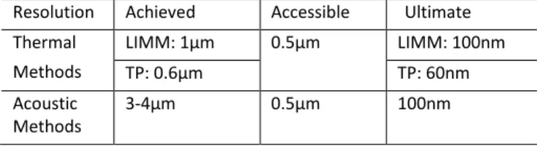
-2 -1 0 1 2 1 2 3 10s 30s 1min 2min 5min Position (µm) K F M p ro fi le ( V ) (a) 0 100 200 300 0.0 0.5 1.0 1.5 2.0 2.5 3.0 Vm . I FWHM Injection time (s) Vm ( V ) a n d a re a I ( V .µ m ) 0.0 0.2 0.4 0.6 0.8 1.0 F W H M ( µ m ) (b)
Figure 2. (a) KFM profile after charging under 20V during different times in
SiOxNy γ=100 layer. (b) Evolution of maximum potential Vm, area under peak
and FWHM as function of injection time.
Figure 1 emphasizes that each layer exhibits proper behavior. For γ=100 and γ=5 charges are stored close to the injection point (FWHM=0.9 and 4.6µm, respectively) whereas γ=10 layer exhibits strong lateral charges spreading (FWHM=37µm). Figure 2a shows the influence of injection time on KFM profile for γ=100 layer. One should recall here that γ=100 layer presents highly insulating properties, close to those of thermal SiO2 layer, which actually limit the charge
transport. No real shape modification is induced when increasing the charging time (Fig. 2a). Figure 2b represents the evolution of the spot profile parameters with charging time. A
4 saturation of injected charge is observed with increasing charging time (results not shown), whereas the FWHM is quite constant. Quite the same behavior is observed for γ=5 whereas, in γ=10 layer, the charge spot broadens and grows without saturation effect with charging time [23].
Thorough analysis of the obtained results provides information on the evolution of the charge cloud behavior and infers possible decay mechanisms and trapping processes [32]. However, more work needs to be done to further understand contrasts observed by KFM on these dielectric layers. In addition, quantitative determination of charges using KFM measurement is difficult due to complications inherent to KFM modeling [14]. In-depth localization of the injected charges is impossible. In spite of these limitations, surface potential measurements by KFM have become a standard for exploring injection, trapping and transport of charges in insulating thin films.
4 ELECTROSTATIC FORCE DISTANCE CURVE: A
NEW WAY TO PROBE SPACE CHARGE4.1 EFDC PRINCIPLE
Electrostatic Force Distance Curve method is based on FDC technique which consists in measuring the evolution of the interaction force between tip and sample as a function of their separation distance. As shown on Fig. 3, the procedure consists of three phases, an approach phase, a jump to contact due to the Van der Waals forces and a contact step. An applied bias on the AFM tip modifies the curve shape and more particularly the approach phase reflecting the fact that the electrostatic force is a long-range force. The electrostatic force can be extracted from these measurements by taking the difference in the force curves with and without potential application on the tip (inset in Fig. 3).
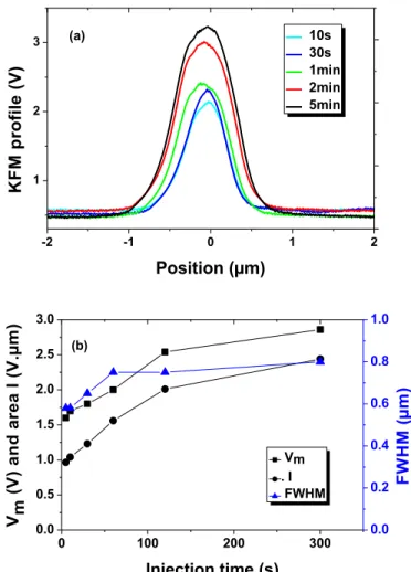
It must be stressed that the electrostatic force does not vary as the square of the distance as one might expect of an electrostatic force. This is mainly due to the fact that the electrostatic configuration is not plane-plane but tip-plane (typical tip radius being between 5 nm and 120 nm). The EFDC is actually sensitive to tip characteristics, contrary to potential measurement by using KFM.
Figure 4 shows the influence of the AFM probe spring constant and radius of curvature on the EFDC shape for 15V applied on tip. It is observed that the curve shape is greatly influenced by the curvature radius while the baseline (long range force) varies a little. Indeed, when the curvature radius decreases, the maximum force decreases, and the jump to contact becomes more abrupt. Moreover, the baseline is more influenced by cantilever spring constant. For the same curvature radius, the shape of the curve is the same as the baseline is more important for low spring constants.
The cantilever spring constant (k) depends on the geometrical parameters, such as its length and width. In particular, k decreases with cantilever surface increasing. Therefore, the base line represents the cantilever contribution to the electrostatic force at a distance far from the surface
(typically the height of the tip, of the order of 10µm). It therefore appears that the shape of the curve is influenced by the curvature radius while the base line is more sensitive to the spring constant.
To characterize EFDC curve two parameters can be extracted: baseline which corresponds to the long-range force contribution and maximum force which is the force at jump to contact. 0.0 -0.5 -1.0 -1.5 -2.0 -100 -80 -60 -40 -20 0 20 40 Approach No bias 25V on tip F o rc e (n N ) Tip-sample distance (µm) Jump to contact 0.0 -0.5 -1.0 -1.5 -2.0 -100 -80 -60 -40 -20 0 F o rc e (n N ) Tip-sample distance (µm)
Figure 3. Influence of tip bias on the EFDC shape. In inset, resulting
electrostatic force for 25V applied on tip.
0.0 0.5 1.0 1.5 2.0 -60 -40 -20 0 k=0.44N/m and Rc=120nm k=2.5N/m and Rc=112nm k=0.44N/m and Rc=5nm k=2.5N/m and Rc=60nm Tip-sample distance (µm) E le c tr o s ta ti c F o rc e ( n N )
Figure 4. Influence of the AFM tip characteristics (curvature radius and
spring constant) on EFDC shape for 20V applied on the tip.
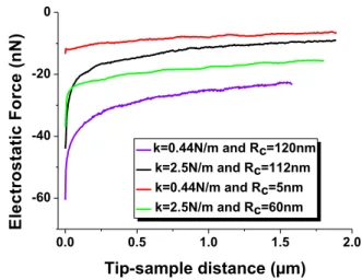
Figure 5 shows the evolution of the maximum force (occurring at contact point) as a function of the square of the applied voltage. First of all, the maximum force increases approximately linearly with the square of the potential. The slope of the line provides a trend regarding the sensitivity of the technique as a function of tip characteristics. Obtained results highlight that sensitivity is improved in tips with large curvature radius. Moreover, cantilever spring constant influences the detection threshold (minimum force that can be detected). Indeed, the electrostatic force Fe is related to
cantilever deflection δ by the spring constant k according to the relation:
5 For a fixed force, the deflection amplitude is divided by a factor of 10 if the spring constant is multiplied by a factor of 10. It will therefore be easier to detect small forces with low spring constant. In what follows, an AFM tip with a radius of curvature Rc = 60 nm and stiffness coefficient of 0.44N/m was
used. 0 200 400 600 800 1000 -120 -100 -80 -60 -40 -20 0 k=0.44N/m et Rc=120nm k=2.5N/m et Rc=112nm k=0.44N/m et Rc=5nm k=2.5N/m et Rc=60nm F e m ax (n N )
Square of applied voltage (V2)
Figure 5. Evolution of the maximum force as a function of the square of
applied bias V².
These results demonstrate that EFDC measurements can be the base of a highly sensitive technique for measuring electrostatic forces induced by the applied bias, however the method is strongly dependent on the probe characteristics. Recently, the electrostatic force was successfully modeled using finite volume technique [33] which reinforces the suggestion that the EFDC method is a promising method to investigate injected charges.
4.2 PROBING OF CHARGE INJECTION BY EFDC
Charging was realized following the same protocol as for KFM studies to achieve comparison between the two techniques. Indeed, charge injection is carried out by bringing the tip into contact with the surface and applying a potential difference for a variable time. The electrostatic force is then measured at different sites on the surface as shown in Fig. 6. First, one can notice that the shape of the EFDC recorded over the charge spot has similar shape to that obtained with a bias on tip. As mentioned previously, the electrostatic force does not scale up with the distance as a square function. However, in this case, no offset of the force at long distance is detectable, indicating that the electrostatic force induced by the injected charge has attenuated action on the cantilever. This is probably due to the localization of the charges, at the origin of the forces, in a small spot. Moreover, EFDC shape and maximum force vary with the distance between the measurement point and the injection point. The maximum and the curvature of the EFDC decrease with the distance from the injection point. Consequently, EFDC contains more information than that provided by the maximum force. One can exploit this property to extract information about charge localization.
Considering the maximum force profile as a function of the position related to the injection point, a direct comparison with the potential profile measured by KFM on the same charge spot can be done as shown in the inset in Fig. 6. The profile FWHM is almost the same for the two techniques. This tends to show that the estimated width of the charge spot is not impeded by the resolution of the two methods and corresponds to the actual spot size. Therefore, it can be considered that the lateral spatial resolution of both methods is smaller than the spot size. Additional information is expected to arise after exploring the shape (curvature) of the EFDC. To extract quantitatively this information on the spatial distribution of charge density, a numerical model is required to describe accurately EFDC induced by hypothetical charge clouds. This 3D Finite Element Model, developed on COMSOL, is in progress having first validation obtained for the applied bias on AFM tip [33]. Extension to the computation of forces induced by 3D- charge clouds stored in the dielectric layer is currently on the way.
0.0 0.2 0.4
-8 -4 0
Position from injection point: 0nm 250nm 500nm 750nm E le c tr o s ta ti c F o rc e ( n N ) Tip-sample distance (µm) -2 -1 0 1 2 0 1 2 0 5 10 F o rc e ( n N ) KFM EFDC P o te n ti a l (V ) Position (µm)
Figure 6. EFDC measurements at different localization over injected charge
spot (charging for 1min under 20V) in γ=100 SiOxNy layer. In inset, KFM and
maximum electrostatic force profiles.
In the following, the influence of charge density and localization are investigated experimentally to highlight EFDC sensitivity. To reach this goal, various charge spots were formed in SiOxNy thin layers with different electrical
properties (i.e. different values of the γ ratio). Charge localization was determined by KFM potential measurement (cf. previous part) to determine the maximum potential and FWHM. Different aspects are under investigation, notably the influence of maximum potential and charge lateral spreading.
To extract information from EFDC curve, electrostatic force as function of distance is fitted by a logistic law:
(2) Where z is the tip-sample distance, is the force when the tip is far from the surface, is the maximum force (tip-surface contact), characterizes the abruptness of the jump to
6 contact ( =0.01 in our case) and p is a parameter describing the EFDC curvature.
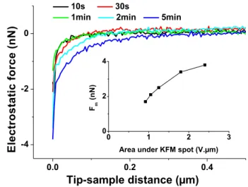
Figure 7 represents EFDC obtained for the same injection conditions as for the results shown in Fig. 2 (different charging times under 20V in γ=100 layer). It is observed that the shape of the curve remains essentially unchanged with the increase of the injection time. Only the maximum force increases. The KFM measurements made on these charge spots show that the maximum potential increases whereas FWHM remains nearly constant, between 0.6 and 0.8µm (Fig. 2). As shown in inset in Fig. 7, the maximum force increases with the area under potential profile which proves the direct link between this parameter and amount of injected charge. The decrease in slope at long charging time is attributed to a sensible spot broadening.
Figure 8 compares EFDC measurements made on three charge spots having different width and the same potential maximum. The maximum and FWHM were determined on KFM profiles shown in Fig. 1. It is observed that the curve shape is modified when the spot size increases. It appears that the curvature is smoother when the spot size is increased. Indeed, parameter p is equal to 1.2, 0.65 and 0.45 for FWHM of KFM spot of 0.6µm, 6µm and 16.5µm respectively. Furthermore, the maximum force increases with the FWHM of KFM profile, which is due to an increase of the amount of stored charges. This is confirmed in a previous study [34] highlighting that curvature, represented by p, is linked to charges lateral spreading and maximum force is related to charge amount (potential maximum and width of charge distribution).
To address EFDC in depth sensitivity, electrostatic force measurements were performed on buried electrodes of different width. Table 2 compares maximum force and p for three different electrodes (width and applied potential) buried at a depth of 10nm, 50nm or 100nm- in SiOxNy. These results confirm that curvature is influenced by the lateral expansion of the charged region. Moreover, p has the same value for charge spot or electrode of 6µm-width.
Concerning maximum force, results emphasize that Fm is
sensitive to applied bias and electrode vertical localization. Indeed, electrostatic force decreases with electrode depth increasing. So these results demonstrate that EFDC is sensitive to in depth charges localization.
Table 1. Evolution of p and maximum force Fm of EFDC measured over
electrode buried at different depths as function of electrode width and bias applied. Depth (nm) Width 6µm 10V applied Width 20µm 10V applied Width 6µm 4V applied 100 p 0.62 0.42 0.61 -24 -31 -6 50 p 0.6 0.42 0.59 -26 -35 -7.8 10 p 0.69 0.46 0.65 -63 -65 -12.4
Even if EFDC shape sensitivity to charges localization is demonstrated experimentally, modelling of electrostatic force appears essential in order to extract the various contributions. According to superposition principle, extraction of space charges profile from EFDC measurement is theoretically possible but not trivial. The first step is to develop accurate modelling of electrostatic force taking into account tip shape and to realize a parametric study on the influence of trapped charge features (density, distribution shape, in-depth localization…) on the EFDC. The second step will consist in the development of inverse method permitting charges density extraction from EFDC curves over charges spot (as on figure 4). The unicity of the solution is not guaranteed at present; however results provided by this method can be coupled e.g. to KFM to level off indetermination.
0.0 0.2 0.4
-4 -2 0
10s 30s
1min 2min 5min
E le c tr o s ta ti c f o rc e ( n N ) Tip-sample distance (µm) 0 1 2 3 0 2 4 Fm ( n N )
Area under KFM spot (V.µm)
Figure 7. EFDC recorded after charging γ=100 SiOxNy layer with AFM tip
under 20V for times indicated in the legend. In inset, evolution of the maximum force as a function of the area under KFM spot which represents in first approximation the charge density.
0.0 0.5 1.0 1.5 -4 -3 -2 -1 0 =100 - FWHM = 0.5µm =5 - FWHM = 5µm =10 - FWHM = 15.8µm Tip-sample distance (µm) E le c tr o s ta ti c f o rc e ( n N )
Figure 8. Influence of the charge profile FWHM on EFDC at injection point
(KFM maximum potential is 0.9V; results obtained with different SiOxNy
7
5
EFDC AND KFM RELATIVE MERIT FOR
SPACE CHARGE MEASUREMENT
To compare KFM and EFDC methods, three aspects are compared: reproducibility, in depth sensitivity and charges extraction strategy.
Concerning measurement reproducibility, the protocol for charges injection was repeated five times at different location and EFDC and KFM were performed each time. Concerning KFM measurement a standard deviation of 8% for maximum potential and of 4% for FWHM was extracted. Concerning EFDC a standard deviation of 4% for maximum force and 7% for p was extracted [34]. So these two methods seem to have comparable reproducibility. This conclusion could be limited by the fact that EFDC is more sensitive to tip shape than KFM. But, as charges injection is strongly influenced by tip shape (the curvature radius controls the electric field at injection point) [35], the tip needs to be well characterized whatever measurement technique is used when localized charges injection is investigated.
Results presented above highlight that EFDC should provide more information than KFM in terms of space charge localizationthrough its sensitivity to in-depth charges localization. Concerning charges density extraction from KFM measurement, two kinds of models have been developed, taking into account or not the fact that KFM is not sensitive to image charges [14, 36]. To extract charge densities from these models strong hypotheses are needed concerning charge distribution in the vertical direction, as e.g. homogeneous distribution or Gaussian distribution, which induce a 50% of variation on charges density value [36]. Concerning EFDC, charges density extraction from curve is not demonstrated, but results present here are promising. Even if the solution unicity is not guaranteed a comparison between results provided by KFM and EFDC could approach charges density in 3D.
Regarding practical implementation, the EFDC measurement is more time-consuming than the KFM one because the force distance curve must be acquired point-by-point before data processing. This feature is not restrictive because dedicated software for data acquisition (which can be implemented in Peak-Force mode, for example) can solve this issue. The most restrictive aspect of EFDC method is the intrusiveness of measurement. Indeed, during electrostatic force measurement the grounded AFM tip is in contact with the sample surface which alters spot charges by inducing charges quantity decrease. Reducing contact force and time in contact permits to limit this effect. Moreover, the time between two consecutive measurements (typically 5min) should be increased to avoid discharging effect by the tip. This is restrictive for charges decay investigation [23], but not crippling for the slow discharging dynamic observed classically in dielectric.
Even if the EFDC technique is somewhat heavier to implement than the KFM one, especially for drawing profiles from different positions on a charge spot, EFDC appears very promising for the study of the density of space charge due to
its sensitivity to charges localization.
6 CONCLUSION
In this study KFM and EFDC methods were presented and compared as tools to probe space charges in thin dielectric layers at nanometer scale. The information gained is not as direct as that resulting from acoustic or thermal methods, based on perturbation of the equilibrium between electrostatic and elastic forces. However, the nanoscale resolution is not at reach at the present time with these classical methods. KFM provides quick and interesting results about charges localization at the surface of the sample; however the lack of sensitivity on in-depth localization is limiting. Contrary to KFM, EFDC is a point-by-point technique which probes directly the electrostatic forces induced by localized charges. The main advantages of this method compared to KFM are its sensitivity to charge distribution and the fact that EFDC can be easily modelled. These studies are currently underway aiming at quantifying the in-depth resolution of the EFDC. Indeed, the purpose is not only to image charges, but to obtain quantitative information on their density. For this, the development of a 3D model of the electrostatic force is required. Our recent works show a good match between the simulated and measured forces on biased tip, and the next and indispensable step will be to extract quantitatively the charges density.
ACKNOWLEDGMENT
This work has been supported by Région Midi-Pyrénées under contract Reference 10051265.
REFERENCES
[1] R. Gerhard-Mulhaupt and M.C. Joseph, Electrets 3rd edn (California: Laplacian Press) 1999
[2] A. Witvrouw, H.A.C. Tilmans, and I. De Wolf, “Materials issues in the processing, the operation and the reliability of MEMS”, Microel. Engg 76, 245–257, 2004.
[3] R.J. Fleming, “Space Charge Profile Measurement Techniques: Recent Advances and Future Directions”, IEEE Trans. Dielectr. Electr. Insul. 12, 967, 2005
[4] S. Holé, “Resolution of Direct Space Charge Distribution Measurement Methods”, IEEE Trans. Dielectr. Electr. Insul. 15, 861, 2008
[5] G. Dagher S. Holé, and J. Lewiner, “A Preliminary Study of Space Charge Distribution Measurements at Nanometer Spatial Resolution”, IEEE Trans. Dielectr. Electr. Insul. 13, 1036, 2006.
[6] M Arnaout, F Baudoin, L Berquez, and D Payan, “Study of signal treatment for a pulsed electro-acoustic measurement cell: a way of improving the transfer matrix condition number”, J. Phys. D: Appl. Phys. 44, 405403, 2011
[7] A. Petre, C.D. Pham, D. Marty-Dessus, and L. Berquez, “Three-dimensional space charge cartographies by FLIMM in electron irradiated polymers”, J. Electrostat. 67, 430, 2009.
[8] G. Teyssedre, C. Villeneuve, L. Boudou and K. Makasheva, “Challenges in probing space charge at sub-micrometer scale”, Annual Report Conf. Electrical Insulation and Dielectric Phenomena (CEIDP, p. 234-237), 2012.
[9] C. Schönenberger, “Charge flow during metal-insulator contact” Phys. Rev. B 45, 861, 1992.
[10] C. Schönenberger and S.F. Alvarado, “Observation of single charge carriers by force microscopy”, Phys. Rev. Lett. 65, 25, 1990.
8 [11] T. Melin H. Diesinger, D. Deresmes, and D. Stiévenard, “Electric force
microscopy of individually charged nanoparticles on conductors: An analytical model for quantitative charge imaging”, Phys. Rev. B 69, 035321, 2004.
[12] J. Lambert, C. Guthmann, and M. Saint-Jean, “Relationship between charge distribution and its image by electrostatic force microscopy”, J. Appl. Phys. 93, 5369–5376, 2003.
[13] C.A. Rezende, R.F. Gouveia, M.A. da Silva, and F. Galembeck, “Detection of charge distribution in insulator surfaces”, J. Phys.: Condens. Matter 21, 263002, 2009.
[14] E. Palleau, L. Ressier, Ł. Borowik, and T. Mélin, “Numerical simulations for quantitative analysis of AFM electrostatic nanopatterning on PMMA by Kelvin Force Microscopy”, Nanotechnology 21, 225706, 2010.
[15] B. Cappella and D. Dietler, “Force-distance curves by atomic force microscopy”, Surf. Sci. Rep. 34, 1–104, 1999.
[16] S. Gomez-Monivas, L. S. Froufe-Perez, A. J. Caamano, and J. J. Saenz, “Electrostatic forces between sharp tip and metallic and dielectric surface”, Appl. Phys. Lett. 79, 24, 2001.
[17] S. Patil and C. V. Dharmadhikari, “Investigation in the electrostatic forces in scanning probe microscopy at low bias voltage”, Surf. Interface Anal. 33, 155, 2002.
[18] Y. Kim, Y.I. Yang, I. Choi, and J. Yi, “Dependence of approaching velocity on the Force-Distance curve in AFM”, Korean J. Chem. Engg. 27, 324, 2010.
[19] M.G. Jenke C. Santschi, and P. Hoffmann, “Two-dimensional electrostatic force field measurement with simultaneous topography measurement on embedded interdigitated nanoelectrodes using FDC”, Appl. Phys. Lett. 92, 063113, 2008.
[20] J. Colchero, A. Gil, and A.M. Baro, “Resolution enhancement and improved data interpretation in electrostatic force microscopy”, Phys. Rev. B 64, 245403, 2001.
[21] T.S. Gros, C.M. Prindle, K. Chamberlin, N. bin Kamsah, and Y. Wu, “Two-dimensional, electrostatic finite element study of tip-substrate interactions in electric force microscopy of high density interconnect structure”, Ultramicroscopy 87, 147, 2001.
[22] K. Makasheva, B. Despax, L. Boudou, and G. Teyssedre, “Dielectric Layers for RF-MEMS Switches: Design and Study of Appropriate Structures Preventing Electrostatic Charging”, IEEE Trans. Dielectr. Electr. Insul. 19, 1195–1202, 2012.
[23] C. Villeneuve-Faure, K. Makasheva, C. Bonafos, B. Despax, L. Boudou, P. Pons, and G. Teyssedre, “Kelvin force microscopy characterization of charging effect in thin a-SiOxNy:H layers deposited in pulsed plasma enhanced chemical vapor deposition process by tuning the Silicon-environment”, J. Appl. Phys. 113, 204102, 2013.
[24] B. Cappella and G. Dietler “Force-distance curves by atomic force microscopy” Surface Sci. Reports Vol. 34 , pp. 1-103, 1999.
[25] T. Mélin, M. Zdrojek, and D. Brunel, in Scanning Probe Microscopy in Nanoscience and Nanotechnology, Part 1. p. 89-128, Springer-Verlag Berlin Heidelberg, (2010).
[26] H.O. Jacobs, P. Leuchtmann, O.J. Homan, and A. Stemmer, “Resolution and contract in Kelvin Probe force microscopy”, J. Appl. Phys. 84, 1168, 1998.
[27] U. Zaghloul, G.J. Papaioannou, F. Coccetti, P. Pons, and R. Plana, “A systematic reliability investigation of the dielectric charging process in electrostatically actuated MEMS based on Kelvin probe force microscopy”, J. Micromech. Microeng. 20, 064016, 2010.
[28] D. Ziegler, N. Naujoks, and A. Stemmer, “Feed-forward compensation of surface potential in atomic force Microscopy”, Rev. Sci. Instrum. 79, 063704, 2008.
[29] D. Ziegler and A. Stemmer, “Force gradient sensitive detection in lift-mode Kelvin probe force microscopy” Nanotechnology 22, 075501, 2011.
[30] W.R. Silveira and J.A. Marohn, “Microscopic View of Charge Injection in an Organic Semiconductor”, Phys. Rev. Lett. 93, 116104, 2004 [31] S. Morita, T. Uchihashi, K. Okamoto, M. Abe, and Y. Sugawara,
Microscale Contact Charging on Silicon Oxide in Characterization, Nanofabrication and Device Application of Functional Materials, edited by P. M. Vilarinho et al. (Kluwer Academic Publishers, 2005), Vol. 186, pp. 289–308.
[32] S.-D. Tzeng and S. Gwo, “Charge trapping properties at silicon nitride/silicon oxide interface studied by variable-temperature electrostatic force microscopy,” J. Appl. Phys. 100, 023711, 2006.
[33] A. Boularas, F. Baudouin, G. Teyssedre, C. Villeneuve, S. Clain, “Multi-dimensional modelling of electrostatic forces over dielectric surface: influence of tip geometry and correlation with experiment” J. Appl. Phys. 116, 084106, 2014.
[34] C. Villeneuve-Faure, L. Boudou, K. Makasheva, and G. Teyssedre “Towards 3D charge localization by a method derived from atomic force microscopy : the electrostatic force distance curve“, J. Phys. D: Appl. Phys. 47, 455302, 2014.
[35] K. Makasheva, C. Villeneuve-Faure, C. Laurent, B. Despax, L. Boudou, and G. Teyssedre “Dielectric charging by AFM in tip-to-sample space mode: overview and challenges in revealing the appropriate mechanisms” Nanotechnology 26, 295704, 2015.
[36] D.S.H. Charrier, M. Kemerink, B. E. Smalbrugge, T. Vries, and R.A.J. Jansen “Real versus measured surface potentials in scanning Kelvin probe microscopy”, ACS Nano 2, 622, 2008.
Christina Villeneuve-Faure was born in Montauban, France in 1981. She received an engineering degree in materials and nanophysics from Institut National Polytechnique Grenoble in 2004 and PhD degree in material physics from the University of Toulouse in 2007. After 4 years post-doctoral position in LAAS-CNRS on MEMS reliability she is, since 2011, associate professor in LAPLACE, France. Her researches focus on AFM characterization of electrical properties of thin dielectric and semiconductor films.
Laurent Boudou was born in Figeac, France in
1975. He received the M.Sc. degree in electrical engineering in 1998, and the Ph.D. degree in 2001 from Toulouse University. He is actually assistant professor at the Toulouse University and is leading researches in the field of electrical properties of polymeric materials at LAPLACE. He has worked on low current measurement techniques applied to polymers and is currently involved in electrical and physico-chemical characterization of different materials, from polymers to thin dielectric plasma deposits, for different applications from high power insulated cables to Micro-Electro-Mechanical Systems.
Kremena Makasheva has obtained the Ph.D.
degree from Sofia University, Bulgaria in 2002 for her work on surface wave sustained discharges. In 2003 she joined the Groupe de physique des plasmas at Université de Montréal, Québec for almost 4 years to work on surface wave discharges at atmospheric pressure and especially to study the contraction phenomenon of gas discharges. In 2007 she joined LAPLACE laboratory in Toulouse, France. Since 2009 she has been working on deposition of thin dielectric layers by plasma processes, their characterization and analysis of the obtained results in relation with dielectric charging phenomenon. She entered the CNRS in 2010. Her research activities now in LAPLACE are directed to the study of reactive plasmas and the design of nanocomposites materials.
Gilbert Teyssedre was born in May 1966 in Rodez, France. He received his
Engineer degree in materials physics and graduated in solid state physics in 1989 at the National Institute for Applied Science (INSA). Then he joined the Solid State Physics Lab in Toulouse and obtained the Ph.D. degree in 1993 for work on ferroelectric polymers. He entered the CNRS in 1995 and has been working since then at the Electrical Engineering Lab (now Laplace) in Toulouse. His research activities concern the development of luminescence techniques in insulating polymers with focus on chemical and physical structure, degradation phenomena, space charge and transport properties. He is currently Research Director at CNRS and is leading a team working on the reliability of dielectrics in electrical equipment.