HAL Id: hal-01367598
https://hal.archives-ouvertes.fr/hal-01367598
Submitted on 16 Sep 2016HAL is a multi-disciplinary open access archive for the deposit and dissemination of sci-entific research documents, whether they are pub-lished or not. The documents may come from teaching and research institutions in France or abroad, or from public or private research centers.
L’archive ouverte pluridisciplinaire HAL, est destinée au dépôt et à la diffusion de documents scientifiques de niveau recherche, publiés ou non, émanant des établissements d’enseignement et de recherche français ou étrangers, des laboratoires publics ou privés.
The 2014 Magnetism Roadmap
Robert L. Stamps, Stephan Breitkreutz, Johan Åkerman, Andrii V. Chumak,
Yoshichika Otani, Gerrit E. W. Bauer, Jan-Ulrich Thiele, Martin Bowen, Sara
A. Majetich, Mathias Kläui, et al.
To cite this version:
Robert L. Stamps, Stephan Breitkreutz, Johan Åkerman, Andrii V. Chumak, Yoshichika Otani, et al.. The 2014 Magnetism Roadmap. Journal of Physics D: Applied Physics, IOP Publishing, 2014, 47 (33), pp.333001. �10.1088/0022-3727/47/33/333001�. �hal-01367598�
1
This topical review is published in J. Phys. D: Appl. Phys. (FREE ARTICLE):
http://iopscience.iop.org/0022-3727/47/33/333001
The 2014 Magnetism Roadmap
Robert L Stamps
1, Stephan Breitkreutz
2, Johan Åkerman
3,4, Andrii V Chumak
5, YoshiChika
Otani
6,7, Gerrit E W Bauer
8,9, Jan-Ulrich Thiele
10, Martin Bowen
11, Sara A Majetich
12, Mathias
Kläui
13, Ioan Lucian Prejbeanu
14,15,16, Bernard Dieny
14,15,16, Nora M Dempsey
17,18and Burkard
Hillebrands
51 School of Physics and Astronomy, University of Glasgow, Glasgow, UK, G12 8QQ
2 Technische Universität München, Lehrstuhl für Technische Elektronik, Arcisstrasse 21, Munich, 80333, Germany 3 Department of Physics, University of Gothenburg, Fysikgränd, Gothenburg, 41296, Sweden
4 KTH-Royal Institute of Technology, Materials Physics, Electrum 229, Kista, 164 40, Sweden
5 Fachbereich Physik, Technische Universität Kaiserslautern, Erwin-Schrödinger-Str. 56, 67663 Kaiserslautern, Germany 6 Institute for Solid State Physics, The University of Tokyo, Kashiwanoha 5-1-5, Kashiwa, Chiba, 277–8581, Japan 7 Quantum Nano-Scale Magnetism Team, Center for Emergent Matter Science (CEMS), RIKEN, 2-1 Hirosawa, Wako 351-0198, Japan
8 Institute for Materials Research and WPI-AIMR, Tohoku University, Aoba-ku, Katahira 2-1-1, Sendai 980–8577, Japan 9 Kavli Institute of Nanoscience Delft, Delft University of Technology, Lorentzweg 1, 2628 CJ Delft, The Netherlands 10 Seagate Technology, 47010 Kato Road, Fremont, CA, 94538, USA
11 Institut de Physique et Chimie des Materiaux de Strasbourg, CNRS-U. de Strasbourg, UMR 7504, 23 rue du Loess, BP 43, F-67034 Strasbourg Cedex 2, France
12 Department of Physics, Carnegie-Mellon University, 5000 Forbes Avenue, Pittsburgh, PA, 1521, USA
13 Institute of Physics and Graduate School of Excellence Materials Science in Mainz, Johannes Gutenberg Universität Mainz, Staudinger Weg 7, 55128, Mainz, Germany
14 Univ. Grenoble Alpes, INAC-SPINTEC, F-38000 Grenoble, France 15 CEA, INAC-SPINTEC, F-38000 Grenoble, France
16 CNRS, SPINTEC, F-38000 Grenoble, France
17 Univ. Grenoble Alpes, Inst NEEL, F-38042 Grenoble, France 18 CNRS, Inst NEEL, F-38042 Grenoble, France
E-mails: [email protected], [email protected], [email protected] / [email protected],
[email protected], [email protected], [email protected], [email protected],
[email protected], [email protected], [email protected], [email protected], [email protected],
[email protected] and [email protected]
Abstract
Magnetism is a very fascinating and dynamic field. Especially in the last 30 years it has experienced many major advances in the full range from novel fundamental phenomena to new products. Applications such as hard disk drives and magnetic sensors are part of our daily life, and new applications, such as in non-volatile computer random access memory, are expected to surface shortly. Thus it is timely for describing the current status, and current and future challenges in the form of a Roadmap article. This 2014 Magnetism Roadmap provides a view on several selected, currently very active innovative developments. It consists of 12 sections, each written by an expert in the field and addressing a specific subject, with strong emphasize on future potential.
This Roadmap cannot cover the entire field. We have selected several highly relevant areas without attempting to provide a full review – a future update will have room for more topics. The scope covers mostly nano-magnetic phenomena and applications, where surfaces and interfaces provide additional functionality. New developments in fundamental topics such as interacting nano-elements, novel magnon-based spintronics concepts, spin-orbit torques and spin-caloric phenomena are addressed. New materials, such as organic magnetic materials and permanent magnets are covered. New applications are presented such as nano-magnetic logic, non-local and domain-wall based devices, heat-assisted magnetic recording, magnetic random access memory, and applications in biotechnology.
2
Contents
Interacting nanoelements and nanostructures (Robert L Stamps)
3
Nanomagnetic logic (Stephan Breitkreutz)
6
Spin torque oscillators (Johan Åkerman)
9
Magnon spintronics (Andrii V Chumak)
12
Non-local based devices (YoshiChika Otani)
15
Spin caloritronics (Gerrit E W Bauer)
18
Heat-assisted magnetic recording (Jan-Ulrich Thiele)
20
Developing synergies between organic and spin electronics (Martin Bowen)
23
Magnetic nanoparticles for biomedicine (Sara A Majetich)
26
Domain wall based devices (Mathias Käui)
29
Magnetoresistive random-access memory (Ioan Lucian Prejbeanu, Bernard Dieny)
32
3
Interacting
nanoelements
and
nano-structures
Robert L Stamps, University of Glasgow
Status
–
Microelectronics is an example of how new functionalities emerge from engineered combinations of carefully chosen material building blocks. Interfaces govern interactions between the building blocks, and much of the technological innovation and evolution of solid state devices has followed improvements in thin film and heterostructure growth capabilities to sculpt and control interfaces. This, together with improved technologies to create complex microstructured platforms, has enabled reliable and economical integration of metallic, semi-conducting and oxide components into robust devices.Fabrication technologies are now being extended to the broad class of ferroic materials, including magnetic elements, alloys and compounds. Advances in lithography used for defining and shaping interfaces in these materials have created new directions for materials development. Response to electric and magnetic fields are of particular importance for many applications, and functional ferroics containing magnetic components offer useful properties for electronic, optical and radio frequency applications. Examples of applications for ferroic composites include sensors, transducers, filters, oscillators, and spintronic devices and information storage.[1] A full description of electric field effects observed in magnetic systems is beyond the scope of the present article, and for the remainder we focus on magnetic examples only.
The breadth of new directions and possibilities enabled by controlled patterning is nicely illustrated with schemes for magnetic based logic. An early approach for magnetic logic was based on the control of domain wall movement in special wire geometries and arrays of coupled magnetic nanoelements.[2,3] Also, spin wave based logic gates were envisaged, utilising spin wave interferometry. An example of a one-input NOT gate was presented in [4] and is based upon manipulation of spinwave phase.
An enticing aspect of this technology is the possibility to create alternatives to semiconducting micro-electronics based computing, with potential for highly efficient, ultra-low power operation. Schemes based upon magnetic reversal can, in principle, operate in the theoretical limit of thermodynamic efficiency, limited only by the entropy of information.[5]
The search for new magnetic materials for spin wave applications has created its own field, now called magnonics. In this field, lithography is used to create arrays of magnetic elements in which high frequency
properties are modified by array design. The precise engineering of composite materials is itself a burgeoning field in that nearly every useful ferroic property can be modified and tuned. Structured composites can be designed to create new advanced materials, and the fruit of this technology will be materials engineering of new, useful, artificial ferroic heterostructures.
Current and Future Challenges
–
One approach to strategic design and engineering of materials is to conceive patterned arrays as mesoscopic artificial ferroic materials. As an example, strong dipolar coupling between nano-magnets has been used to create analogues to solid state magnets. A four sublattice antiferromagnet arrangement, as shown in Figure 1, illustrates two degenerate ground states separated by a boundary arrangement.[6] The arrows represent single domain particles that mimic Ising spins as macroscopic moments with a strong uniaxial anisotropy. This system is an example of an artificial magnet, with mesoscopic spin configurations that may have applications in data storage, computation, and microwave signal processing.[7]The example shown in Figure 1 is a particular realisation of arrangements of magnetic elements that is part of a much larger family of artificial spin systems which encompasses several possible arrangements of dipolar coupled nanomagnets. It is possible to modify magnetization properties and processes in these structures to a degree not imaginable in naturally occurring magnetic systems. An essential and far
Figure 1 – Sketch of ground state configurations for a square array of single domain magnetic elements. The magnetization of an element is represented by green and blue arrows, and the ground state is two-fold degenerate. Examples a,b and c,d illustrate domain growth facilitated by cascading reversals of individual elements. Reversals occur at the circled arrows, and correspond to the flow of magnetic charge represented by the crosses. (Adapted from [6])
4
reaching challenge is the fabrication of perfect sub-micron sized magnetic elements and arrays, and development of methods to manipulate, access, and control their magnetic configurations.
Useful ferroic properties may arise on different time and length scales, and these scales can be controlled through composition and design of elements and arrays. In this way, properties of ferroic structures patterned into single domain elements with individual volumes on the order of 105 nm3, can support responses
to electric and magnetic fields that occur with characteristic times in the range 10-8 to 10-10 s. The key
challenges include finding materials and geometries in which surfaces and interfaces can be precisely defined with at least nanometre dimensions. In this way one can also control thermal stability, and construct systems whose functionality derives from operation near the super-paramagnetic limit, as in phase change applications. Additionally, new materials and approaches are required for scalable microwave frequency applications. Such materials require long spin wave propagation path lengths and miniaturization options for use in integrated circuits.
At present controlled fabrication of composites has been realised only for a few material combinations. Next steps include widening the range of materials and exploring more complicated geometries in three dimensions. Such artificial ferroic systems can be either entirely magnetic or a mixture of magnetic and ferroelectric constituents, and the structure in these systems is created either during thin film growth or with lithographic methods. Such systems would have many degrees of freedom that are much more complex and tuneable than possible with purely ferromagnetic constituents.
Advances in Science and Technology to Meet Challenges
–
Following the concept of new functionality, an important class of polarisable materials incorporating ferroelectric and magnetic materials could emerge because of dielectric polarisation and strain effects. Here the control of interface structure with complex oxide components is critical in order to introduce desired electric and magnetic field responses. Continued refinements are required, including: tuning of materials properties, use of new materials and improvement of coupling at the ferroelectric and magnetic material interface. Advancement here depends very much on improved control of interfaces, construction of thin film heterostructures incorporating complex oxides, and development of robust lithographic techniques for complex geometries.An exciting area of development is concerned with the creation of three dimensional mesoscopic ferroic
systems. The ability to fabricate arrangements of ferroic elements in complex geometries that go beyond planar arrays is challenging, but within reach. Some examples already exist as concepts for ‘racetrack memory’ and ‘magnetic ratchets’ [8,9]. The ratchet concept is based on columnar multilayer elements, and is sketched in Figure 2. In this figure, the formation of solitons in a stack is depicted and indicated by stars. These can be used to represent bits of information and shifted through the stack creating an efficient shift-register in three-dimensional microchips for memory and logic applications.
Further directions impact several different areas. In plasmonics and metamaterials, structures are designed to utilise electromagnetic excitations. For plasmonics, the characteristic length scales of geometrical features should be in the millimetre to micrometre range. A topic to be explored is the incorporation of magnetically polarisable elements in a plasmonic arrays in order to facilitate new and enhanced linear and nonlinear magneto-optical effects [10,11].
Related to this are topics involving charge and spin transport. There are several opportunities for future exploration of transport effects in dipolar coupled magnetic arrays. A particularly exciting direction is the possibility to utilise spin wave excitations in new ways in patterned arrays, as with spin caloritronics in which
spin currents can be created by thermal gradients. Since spin waves carry angular momentum, it has been argued that spin-orbit coupling can affect the transport of angular momentum via spin currents across
Figure 2 – Sketch of magnetic states of a six-layer superlattice constructed with perpendicular films. The blue boxes indicate ‘up’ layer magnetization, and the red boxes are ‘down’ magnetization. The left stacks are the two ground states, and the right stacks are corresponding soliton states that can be ‘ratcheted’ through the stack. Solitons are indicated by the stars. (Adapted from [9])
5
interfaces in some materials. As a consequence, mechanisms originating from spin orbit coupling at interfaces may give rise to spin Seebeck and spin Hall effects, equivalent to their conventional charge transport analogues.[12] This is an exciting and very active area of development at present concerned mainly with thin film structures, but with potentially broad impact on many aspects of magnetization dynamics in patterned nanostructures.
Concluding Remarks
–
The ever increasing requirements for information technology and communications include scalability and high density, which necessarily means small size, faster data storage or transfer, higher output signals, low power consumption, low cost, and reproducible control of the magnetic states. New materials that can be easily integrated into existing technologies will be needed to meet these challenges. Artificial ferroic materials based on interacting modular elements provide many new possibilities with which to meet these challenges. Patterned magnetic multiferroics are technologically relevant because of their susceptibility to electric or magnetic fields, thereby allowing these systems to be implemented as devices for data storage, memory and logic, and radio frequency communications. These materials will be created through precision patterning in two and three dimensions, simultaneously advancing fabrication technology into a higher level and creating novel possibilities and opportunities not possible in single phase materials and thin film heterostructures.References
[1] Nan C W, Bichurin M I, Dong S X, Viehland D and Srinivasan G 2008 Multiferroic magnetoelectric composites: Historical perspective, status, and future directions Journal of Applied Physics 103 031101
[2] Allwood D A, Xiong G, Cooke M D, Faulkner C C, Atkinson D, Vernier N and Cowburn R P 2002 Submicrometer Ferromagnetic NOT Gate and Shift Register Science 296 2003-6
[3] Orlov A O, Amlani I, Bernstein G H, Lent C S, Snider G L 1997 Realization of a Functional Cell for Quantum-Dot Cellular Automata Science 277 928-30
[4] Schneider T, Serga A A, Leven B, Hillebrands B, Stamps R L and Kostylev M P 2008 Realization of spin-wave logic gates Applied Physics Letters 92 022505
[5] Lambson B, Carlton D, Bokor J 2011 Exploring the Thermodynamic Limits of Computation in Integrated Systems: Magnetic Memory,
Nanomagnetic Logic, and the Landauer Limit Phys. Rev. Lett. 107 01064
[6] Budrikis Z, Livesey K L, Morgan J P, Akerman J, Stein A, Langridge S, Marrows C H and Stamps R L 2012 Domain dynamics and fluctuations in artificial square ice at finite temperatures New Journal of Physics 14 035014 [7] Heyderman L J, Stamps R L 2013 Artificial
ferroic systems: novel functionality from structure, interactions and dynamics J. Phys. Condens. Matter 25 363201
[8] Parkin S S P, Hayashi M, Thomas L 2008 Magnetic Domain-Wall Racetrack Memory Science 320 190-4
[9] Lavrijsen R, Lee JH, Fernández-Pacheco A, Petit DC, Mansell R, Cowburn RP. 2013 Magnetic ratchet for three-dimensional spintronic memory and logic Nature 493 647-50 [10] Chen J, Piradeh Z, Alonso-Gonzalez P, Huth F,
Bonetti S, Bonanni V, Akerman J, Nogues J, Vavassori P, Dmitriev A, Aizpurua J, Hillenbrand R 2011 Small 7 2341-2347
[11] Maccaferri N, Berger A, Bonetti S, Bonanni V, Kataja M, Qin Q, van Dijken S, Pirzadeh Z, Dmitriev A, Nogues J, Akerman J, Vavassori P 2013 Phys. Rev. Lett. 111 167401
[12] Uchida K, Xiao J, Adachi H, Ohe J, Takahashi S, Ieda J, Ota T, Kajiwara Y, Umezawa H, Kawai H, Bauer G E W, Maekawa S and Saitoh E 2010 Spin Seebeck insulator Nat Mater 9 894-7
6
Nanomagnetic logic
Stephan Breitkreutz, Technische Universität München Status – Nanomagnetic Logic (NML) is an emerging information processing technology offering nonvolatile logic circuitry to perform boolean and non-boolean operations. Binary information represented by the magnetization state of nanomagnets is processed via field-coupling [1-4]. Nonvolatile majority gate-based logic, low power computing, high density integration, zero leakage and CMOS compatibility are key features of NML. Two different implementations have been developed and established in the research community: In-plane NML (iNML) uses bistable single-domain Pymagnets with shape-dependent in-plane anisotropy arranged in chains and majority gates for logic operation [5]. During clocking, the magnets are forced into a metastable state by a hard-axis clocking field, and, during its removal, switched into their desired state due to fringing field interaction. Meanwhile, the input magnets have to be kept in their desired state to achieve directed signal flow. A 1-bit full adder using slanted-edge magnets has been demonstrated [6]. Perpendicular NML (pNML) uses magnets made of Co/Pt multilayer films showing shape-independent perpendicular magnetic anisotropy (PMA) enabling flexible geometries and circuit designs. The PMA is locally tuned by focused ion beam (FIB) irradiation to create artificial nucleation centers (ANCs) for domain walls (DWs). This technique sets the magnet sensitive to only specific neighbors (inputs) and therefore enables directed signal flow integrated in every single magnet [7]. Information is processed stepwise according to the oscillating easy axis clocking field. For switching and correct ordering of the magnets, the clocking field induced DW nucleation at the ANCs is enforced or prevented by the superposing fringing fields of the input magnets. Recently, a threshold logic gate (TLG)-based 1-bit full adder consisting of only 5 magnets has been realized demonstrating the benefits of pNML circuitry in terms of area and power efficiency [8]. A crossing device using signal detouring through additional functional layers is shown in [9]. Both implementations favor Oersted switching and spin transfer torque (STT) devices as electrical I/O structures for integration in hybrid CMOS/NML circuits. For instance, magnetic tunnel junction (MTJ) structures are well studied for devices with in-plane and perpendicular anisotropy. Integrated on-chip coils and current wires generating sub-µs field pulses are used to supply the clocking field [10,11].
Current and Future Challenges – For both implementations functional elementary circuits have been experimentally demonstrated, therefore current challenges first of all concern the applicability of NML circuitry. NML has to be engineered to meet the key metrics area, power and speed of potential applications.
Hence, research has to focus on material and technological investigations to improve the circuit performance. Additionally, key aspects like signal routing, design and architecture have to be addressed. Area: High density integration is one of the NML key benefits [1]. As the thermal stability of the iNML Py-magnets already reached the 40 kbT border, there seems
to be less potential for further scaling of the magnets themselves [5]. Indeed, design improvements by using the majority decision could further reduce the circuit area [6]. pNML magnets still offer significant scaling potential. Recent publications use magnets with 100 nm width and 30 nm gaps in between [9]. Here, 50 nm wide magnets as demonstrated for magnetic memory devices and 15 nm gaps within logic gates are desirable.
Power: The energy dissipation of NML magnets during switching is in the low aJ-range, so there’s little potential for further improvement. In fact, NML is one of the most promising low-power technologies [1]. Current research in this area should focus on power reduction of the clocking structures, which contribute for major part to total power losses.
Speed: Significant improvements can be gained in the speed of NML circuitry. The (coherent) switching of the iNML magnets occurs below 1 ns, hence GHz clocking frequencies are feasible. By contrast, recent results in pNML indicate working frequencies in the 100 MHz range due to the clocking field generation and the switching process of DW nucleation and propagation [8,10]. Even though data throughput is competitive, speed should be increased to compete with other technologies. For both implementations the required clocking fields also have to allow for GHz operating frequencies.
Figure 1 – Comparison of working principle, majority gate, full adder circuit and clocking structure between in-plane and perpendicular NML [5,6,8,10,11].
7
Signal routing: Active control of signal routing is one key challenge for the realization of complex circuitry. Integrated circuits use multiplexers for signal routing and latches to buffer and synchronize data signals. Also in NML circuits, magnetic signals have to be routed, buffered and synchronized between logic units by directly controllable devices. Thus, applicable latches and multiplexer devices have to be developed.
Architecture: The nonvolatile character of the magnets makes classical von-Neumann architectures with strict separation of logic and memory redundant. Recent research deals with systolic architectures, non-boolean logic and TLG-based circuitry [4,8]. However, controllable memory access plays an important role also in nonvolatile logic circuitry. Therefore, adequate memory cells have to be implemented.
Error rate: One big issue of both NML circuitry is the reliability of magnetic computation that may be impacted due to thermally induced and fabrication variations [8,12]. In addition, the variations of ANCs in pNML circuitry, which are currently manufactured by Ga+ irradiation, are still subject to be reduced.
Controlling variations is the key to reduce error rates for highly integrated systems.
Advances in Science and Technology to Meet Challenges
Material: One of the most potential parameters for significant improvements is the magnetic material itself. iNML is still limited to Py, but pNML offers various options of tunable PMA materials as CoNi or CoFeB [13]. They may reduce fabrication dependent variations resulting in lower error rates. Besides that, smaller switching fields due to a lower anisotropy would also strongly reduce the energy consumption of the clocking structures. Higher DW velocities would increase the clocking frequency.
Technology: Currently, NML structures are fabricated by E-Beam lithography (both) and FIB irradiation (pNML). However, the manufacturability in industrial plants for mass production is still pending. Significant improvement can be achieved in the irradiation technique of the pNML magnets. Lighter He+ FIB
systems or implant technologies with other particles could significantly reduce the variations of the ANCs. Clocking: High permeability low loss claddings for on-chip coils and current wires and enhanced permeability dielectrics (EPD) are currently investigated to reduce the power of integrated NML circuitry [10,11]. Besides common global clocking schemes, innovative clocking concepts using stray fields of propagating DWs to switch nearby magnets seem to be feasible [14], but accurate control of the DWs is required.
Signal routing: Here, pNML seems to be the more appropriate candidate due to its switching process. Accurate control of the DW propagation in magnetic nanowires [15] would enable to specifically block the
signal flow in magnetic interconnects and therefore enable the routing, buffering and synchronization of magnetic information. By contrast, controlling the signal flow in iNML is more challenging due to the coherent magnet switching. Controllable devices (e.g. integrated in the clocking circuitry [11]) for signal routing and buffering have to be developed.
Architecture: There are many architectures suitable for NML, but their implementation in NML is still an open question. The usability of systolic and non-boolean computation is currently only confirmed by simulation [4]. A path breaking success is the realization of 3-dimensional magnetic devices [9]. Since field coupling of NML magnets acts in all spatial directions simultaneously, 3D computing devices are feasible. Concluding Remarks – Currently both NML types demonstrated functional basic circuits and electrical integration proving the feasibility of magnetic and hybrid CMOS/NML circuitry. Considering current and future challenges, pNML seems to be the more appropriate candidate: integrated directed signal flow, tunable anisotropy, arbitrary layout, scalability and controllable signal routing are key parameters for integrated circuitry. Computing reliability and speed still have to be increased to compete with other technologies. Controllable devices for signal routing and buffering are required for iNML. Generally, research has to be intensified on suitable materials and fabrication technologies. Furthermore, efforts should be made to reduce the clocking power losses. A fully-integrated NML system including logic, electrical I/O and on-chip clocking would be desirable for the demonstration of the feasibility of integrated circuits.
iNML pNML
Area: Decrease of circuit
area by majority gate-based design improvements
Reduction of the device & circuit area by scaling of the PMA magnets
Power: Reduction of clocking power by device
improvements or new clocking concepts (e.g. DW- or voltage-based switching)
Speed: Shorter switching
times by material enhancements Higher clocking frequencies by enhanced clocking structures (e.g. use of cladding) or new clocking concepts are required
Signal routing:
Concept for iNML circuitry is needed
Archi-tecture:
- Systolic computing architectures - 3D integration seems to be feasible
Error rate: Limited decrease by signal refreshment - Reduction of the ANC variations - Increase coupling Table 1 – Current and future challenges for NML circuitry and possible solutions to meet the requirements.
8
References
[1] The International Technology Roadmap for Semiconductors: Emerging Research Devices, http://www.itrs.net (2011)
[2] G. Csaba et al., IEEE Transactions on Nanotechnology 1, 209-213 (2002)
[3] M. Becherer et al., Digest Technical Papers IEEE International Solid-State Circuits Conference, ISSCC, 474-475 (2009)
[4] M. Niemier et al., Proceedings of the 13th
International Workshop on Cellular Nanoscale Networks and their Applications, 59-64 (2012) [5] A. Imre et al., Science 311, 205-208 (2006) [6] E. Varga et al., IEEE Transactions on Magnetics
49, 4452-4455 (2013)
[7] S. Breitkreutz et al., Journal of Applied Physics
111, 07A715 (2012)
[8] S. Breitkreutz et al., Joint European Magnetic Symposia (JEMS), Greece (2013)
[9] I. Eichwald et al., IEEE Transactions on Magnetics
49, 4468-4471 (2013)
[10] M. Becherer et al., IEEE Proceedings of the 43rd
European Solid-State Device Research Conference (ESSDERC), 276-279 (2013)
[11] M. T. Alam et al., IEEE Transactions on Nanotechnology 11, 273-286 (2012)
[12] G. Csaba and W. Porod, 14th International
Workshop on Computational Electronics (IWCE), 26-29 (2010)
[13] D. Stanescu et al., Journal of Applied Physics 103, 07B529 (2008)
[14] G. Csaba et al., Journal of Applied Physics 111, 07E337 (2012)
[15] S. Breitkreutz et al., IEEE International Electron Devices Meeting (IEDM), Washington D.C. (2013)
9
Spin torque oscillators
Johan Åkerman, University of Gothenburg and KTH Royal Institute of Technology
Status – Spin torque oscillators (STOs) [1] are broadband microwave signal generators where a direct current excites and controls a magnetodynamic response via the spin transfer torque (STT) [2,3] effect. STOs typically come in one of two principally different architectures: (i) nano-pillars with a diameter of approximately 100 nm diameter, and (ii) nano-contacts (NC), where the current enters an extended magnetic structure through a constriction. While STOs can be based on single ferromagnetic (FM) layers and multilayers, GMR pseudo spin valves (PSVs) and magnetic tunnel junctions (MTJs), with one free and one fixed layer, dominate. It is advantageous for the free layer to be thin and be made of a material with high spin polarization and low spin wave (SW) damping. For these reasons common free layer materials are sputtered Permalloy (Ni81Fe19, here
referred to as NiFe) and various compositions of CoFeB, where the former dominates in GMR based STOs and the latter in MTJ based STOs. Owing to their strongly nonlinear magnetodynamics and variety of SW modes, STOs are both of great fundamental interest and lend themselves to potential applications as nanoscale wideband frequency-tunable and rapidly modulated microwave oscillators for telecommunication, vehicle radar, and microwave spectroscopy applications. Additionally, NC-STOs open up for miniaturized integrated magnonic devices and systems where the generation and control of propagating SWs [4] and the recently discovered magnetic droplet soliton [5] and nano-skyrmion [6] may be utilized for additional functionality.
Current and Future Challenges - While a wide range of STO device architectures have been fabricated and characterized as a function of drive current and magnetic field, the fundamental properties of the underlying magnetodynamic phenomena and the details of the generated spin wave modes still remain largely hidden. The measured microwave voltage is a strongly reduced mapping of a number of possible highly nonlinear, complex, three-dimensional and time-varying magnetization states. While some spatially resolved information have been possible to extract from scanning micro-Brillouin light scattering [4], and XMCD microscopy [7], the most common approach is still to rely on approximate micromagnetic simulations and compare simulated microwave signals with experiments. The smaller dimensions of nano-pillar STOs and the uniformity of the current density allow for good agreement between simulations and experiments and most fundamental aspects are now well understood. The situation is dramatically different
for NC-STOs where much larger simulations must be carried out and where a range of vector and scalar properties are highly non-uniform, such as the current, spin, and heat currents, the spin wave amplitude, and the temperature. The recent advent of powerful GPU accelerated micromagnetic codes have made it possible to reduce the NC-STO simulation times orders of magnitude, resulting in significantly better agreement between simulation and experiments and e.g. some predictive capability of how the non-uniform Oersted field influences the fundamental SW modes underneath the NCs [8]. However, the impact of the non-uniform current density is still largely unexplored, and effective and easy to use fully 3-dimensional simulation tools where both transport and micromagnetics are correctly described are needed. Such simulations will e.g. be critical for modelling single-layer NC-STOs where experiments show that both vortex gyration modes and propagating SW modes can be present and also interact, but likely show different dependence on in- and out-of-plane currents. The recent discoveries of STT generated magnetic droplet solitons [5] and nano-skyrmions [6] also pose additional challenges where additional energy terms such as the Dzialoshinskii-Moria interaction must be properly taken into account in simulations. In addition to improved simulation tools, a better understanding of the spatial and temporal behavior of the generated SW modes will also likely require advances in time-resolved X-ray techniques. For actual applications, three significant drawbacks still limit the usefulness of STOs: (i) their limited output power, (ii) their high phase noise, and (iii) the common requirement of large magnetic fields, in particular for high-field operation, for high-coherence
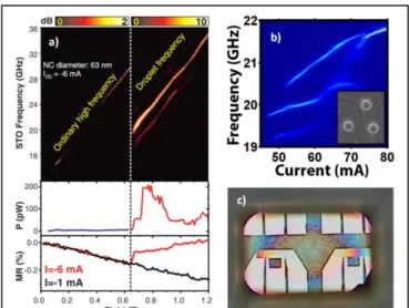
Figure 1 – a) Top view of the wave guide and contact pads of a NC-STO. b) SEM picture of the GMR mesa with openings for a single 100 nm NC in the center and two larger ground contacts to each side. c) Cartoon of the NC-STO material stack. d) Micromagnetic simulation of the spatial extent of the power density of the propagating SW mode (yellow) and the localized SW mode (white). The green circle outlines the NC.
10
signal generation, and for magnonic devices relying on propagating SWs. Whereas a common benchmark number in terms of oscillator output power is “0 dBm”, which in a 50 Ohm system translates to 1 mW, the highest output power achieved in MTJ based STOs is just above 2 µW [9]. The high phase noise is a result of both the small STO mode volume and the strong intrinsic amplitude-phase coupling which transforms and amplifies all amplitude noise into phase noise. High magnetic fields are typically required to increase the local magnetic energy density determining the frequency of the excited spin waves. The highest quality factors, expressed in line width over operating frequency, are also typically realized in high fields and at out-of-plane field angles tilted some 20-30 degrees away from the perpendicular direction.
Advances in Science and Technology to Meet Challenges – The low STO microwave power can be improved upon using a number of approaches. Instead of using GMR in spin valve based STOs, MTJs will have to be used, and their TMR will have to be maximized while simultaneously keeping the resistance-area product (RA) low enough to allow for sufficient current densities to generate coherent auto-oscillations. It will also be necessary to maximize the fraction of the TMR that is actually used by the SW mode. While typical maximum precession angles are of the order of 20 degrees, STOs with perpendicular magnetic anisotropy fixed layers [10] and free layers [11, 12] demonstrate the potential for much larger precession angles. In a similar vein, the recently discovered magnetic droplet soliton [5] can precess at angles of 90 degrees or even higher, i.e. the local spins can precess either in-plane or even against the applied field. Since the STO output power is generated by the variation in resistance during precession, a 90 degree precession angle generates the maximum possible signal. In comparison, a spin precessing at 20 degrees only generates about 12% of that power. Experiments (Fig.2a) indeed demonstrate that the droplet microwave power can be 40 times greater than that of the ordinary precession [5]. If droplets can be generated in MTJ based STOs with a similar increase, the resulting STO power would be about 0.1 mW, i.e. only 10 dB away from the desired 0 dBm level and most likely already sufficient for many applications.
The phase noise can be reduced by increasing the mode volume, e.g. through mutual synchronization of several individual contacts. Recently two important synchronization breakthroughs were reported: i) Maehara et al [9] demonstrated mutual synchronization of MTJ based NC-STOs resulting in both record output power above 2 µW and a quality factor of 850, which is considered high for MTJ-STOs; ii) Sani et al [10] demonstrated mutual synchronization of three
NC-STOs operating above 20 GHz and fabricated using a novel low-cost colloidal lithography approach (Fig.2b). More combined work in these directions will be required to further improve both the output power and phase noise.
On the fundamental side, the still elusive spatial profiles of the various proposed SW modes are currently under intense research by various groups trying to use time-resolved XMCD techniques to acquire direct microscopic information of their spatial extent and wave vector properties. Fig.2c shows an operational NC-STO fabricated on top of a 300 nm SiN membrane currently under investigation using Scanning Transmission X-ray Microscopy and Holographic XMCD with the ambition to directly observe both magnetic droplet solitons and other fundamental SW modes. Alternatively, near-field Brillouin Light Scattering with a resolution of 55 nm [14], and ferromagnetic resonance force microscopy with 100 nm resolution [15], may also help to shed further light on these phenomena.
Concluding Remarks – Spin Torque Oscillators remain a vibrant research field with steady progress both in the fundamental understanding and in raising the microwave performance to levels required by applications. The wealth of dynamical phenomena will continue to inspire theoretical, numerical and experimental work, and provide new insights necessary to better tailor these devices and their underlying material properties, both for microwave generators and spin torque driven magnonic devices and circuits.
Figure 2 – a) A magnetic droplet soliton forms at 0.65 T in a NC-STO with a perpendicular magnetic anisotropy free layer [reprinted with permission from Ref. X]. Power increases by 40x. b) Power spectral density vs. drive current for a three-nano-contact STO. When the three individual signals merge into a single synchronized signal, the total power increases substantially. c) NC-STO fabricated on a SiN membrane for XMCD studies.
11
References
[1] J.-V. Kim, Solid State Physics 63, 217 (2012) [2] J. C. Slonczewski, J. Magn. Magn. Mater. 159, L1
(1996)
[3] L. Berger, Phys. Rev. B 54, 9353 (1996)
[4] M. Madami et al, Nature Nanotechn. 6, 635 (2011) [5] S. M. Mohseni et al, Science 339, 1295 (2013) [6] N. Romming et al, Science 341, 6146 (2013) [7] X.W. Yu et al., Phys. Rev. Lett. 106, 167202
(2011)
[8] R. K. Dumas et al, Phys. Rev. Lett. 110, 257202 (2013)
[9] Maehara et al, Appl. Phys. Exp. 6, 113005 (2013) [10] D. Houssameddine et al, Nature Mater. 6, 441
(2007)
[11] W. Rippard et al, Phys. Rev. B 81, 014426 (2010) [12] Z. Zeng et al, ACS Nano 6, 6115 (2012)
[13] S. R. Sani et al, Nature. Comm. 4, 2731 (2013) [14] J. Jersch et al, Appl. Phys. Lett. 97, 152502 (2010) [15] F. Guo, Phys. Rev. Lett. 110, 017601 (2013)
12
Magnon spintronics
Andrii Chumak, University of Kaiserslautern
Status – Magnons, which are the quanta of the collective excitations of the electrons' spin system – spin waves, was first been predicted by F. Bloch in 1929. Since that time, they are an object of intensive studies oriented towards both fundamental research and application. The wide variety of the linear and non-liner properties as well as the GHz frequency range of magnons used in telecommunication systems, radars, etc., are the main reasons for this interest. The boom in the studies took place after the Yttrium Iron Garnet (YIG) – ferrite with unique small spin-wave losses, was synthesized in 1956. Huge amounts of analog devices for the processing of microwave signals were developed thereafter. Some of them (such as Y-circulators) are still being used today; however, the fast-growing semiconductor technology directed at digital data processing has substituted for the majority. A renaissance of magnon studies is currently being observed. There are several reasons for this: new technologies allowing for operations with magnons at the nano-scale; a number of discovered physical phenomena such as spin pumping or spin transfer torque (STT) and, finally, a need for an alternative to CMOS technologies due to their fundamental limitations. The term magnonics was introduced in 2005 which refers to the transport and processing of data by magnons [1-3]. The usage of magnonics approaches in spintronics (field dealing conventionally with electron-carried spin-currents, see Fig. 1) gave birth to the field of magnon spintronics. There are several advantages which magnons offer to spintronics: (1) Magnons allow for the transport and processing of spin information without the movement of any real particles such as electrons and, therefore, without the generation of Joule heat. (2) The free path of magnons is usually several orders of magnitude larger compared to the spin diffusion length in metals and thus allow for the transport of spin information over macroscopic distances. (3) Finally, the wave nature of spin waves and their abundant non-linear properties provide access to new and more efficient concepts for data processing. Current and Future Challenges – Here, studies which are of major importance to the field are listed. o New approaches for combining magnonics with spintronics and electronics. The general concept of magnon spintronics is shown in Fig. 1. The conversion from charge- and spin-currents to magnons and vice versa allows for the combination of different technologies and are of paramount importance. A rather promising type of conversion is based on the combination of spin pumping, STT, and the (inverse)
spin Hall effect [4-7]. This approach allows for the conversion by placing a several nanometer-thick non-magnetic metal on top of magnon conduits. Moreover, STT allows for the amplification and generation of magnonic currents [6, 7].
o New magnetic materials for magnonics. Magnonics is strongly coupled to Material Science since it requires media with small magnetic damping. The most commonly used materials are Permalloy [3, 8] and YIG [2], but the development of new materials is crucial. For example, it has been shown recently that half-metallic Heusler compounds might be an excellent choice for magnonics not only due to the small damping but also due to the high saturation magnetization and relatively high Curie temperature. o Artificial magnetic materials. Over the last years there have been major achievements in the development and studies of artificial materials with periodic variations of magnetic properties – magnonic crystals. It has been shown that these crystals allow for guiding, filtering, and even short-time storage of magnons on the macro- and micro-scales [2, 3, 8]. Thus, magnonic crystals are very promising for the realization of reconfigurable data processing units. Further achievements in the realization of nano-sized and three-dimensional crystals are expected.
o Minituarization and increase in the operating frequency. Decrease in sizes is of highest priority not only for all-metallic magnonics, but also for low-damping YIG devices. Several groups have very recently reported on the growth and usage of high-quality YIG films of nanometer thickness (starting from 4 nm). We have also studied magnons in nanometer-thick YIG waveguides with lateral sizes of a few microns [9]. Decrease in the sizes of structures and spin-wave wavelengths will automatically result in the increase of the spin-wave frequency due to the positive slope of the dispersion of exchange magnons. The minimum wavelength is limited by the lattice constant of a magnetic material, while the maximum magnon frequency reaches the THz range.
Figure 1 – The concept of magnon spintronics: Infor-mation coded into charge- or spin-currents is converted into magnon flows, processed within the magnonic system and converted back. The wave nature of the magnon flow is used for fast processing of complex data inputs.
13
o Digital data processing. Initial steps in the processing of digital information by magnons were taken recently [10]. One of the earliest realizations of a proof-of-principle XNOR logic gate is shown in Fig. 2. A DC current is used to manipulate spin waves and wave interference to perform logic operations. Another promising approach of the coding of information into the spin-wave’s phase rather than in its amplitude was proposed by A. Khitun [11]. Furthermore, we have demonstrated that the magnons’ natural non-linearity can be used in order to manipulate one magnon with another. A magnon transistor for all-magnon data processing on a single magnetic chip was shown. However, the combination of several logic elements into one magnonic circuit still needs to be realized. o New data processing concepts based on linear and non-linear magnon properties. One of the greatest advantages of magnonics is the possibility to utilize the wave properties at the nanoscale, while most waves of other nature (such as X-rays) are practically inapplicable. This provides access to new data processing concepts in which operations with clusters of information rather than with single bits are used. For example, the linear time reversal of a complex wave packet by a single operation was shown [12]. Fast dynamic magnetic media and nonlinear spin-wave effects suggest huge opportunities for future studies. o Magnon manipulation and generation by electric fields. CMOS technology has shown that the manipu-lation of information by electric fields consumes minimum power. Besides in the (multi)ferroic-like approaches used in the manipulation of magnons (see for example studies of B. Kalinikos [13]), there is a special interest in the manipulation of magnetic anisotropy in ultrathin films. The group of Y. Suzuki has recently demonstrated low power ferromagnetic resonance excitation by an electric field [14]. Other promising approaches are based on Dzyaloshinskii-Moria interactions but are in the initial stages of development.
o Data buffering. Magnons are dynamic objects which require external energy to compensate their damping and are not the best choice for long-term storage of information. Nevertheless, for data processing short term buffering is also required (see Fig. 1). It was shown that the buffering of information carried by magnons is possible for several micro-seconds using slow magnon modes [2].
o Magnon caloritronic effects. In conventional electronics the parasitic heat is ultimately lost. Magnonic systems are also dissipative, but the magnon-phonon interactions are much more sophisticated and include different mechanisms. The very new field of spin caloritronics searches for ways to control or even utilize the parasitic heat [15].
o Quantum effects and Bose-Einstein condensation (BEC) of magnons. Magnons are bosons with a spin equal to one. It has been shown that magnons can form BEC at room-temperature if the density of the injected magnons is high enough. Currently, there are first attempts to use BEC for the transport and processing of spin information in a form of magnon super-currents. Other operations which are carried by a single magnon and the related quantum effects are also of great importance but so far remain beyond realization. Advances in Science and Technology to Meet Challenges - In general, most of the ingredients required for the successful realization of the intended aims facing magnon spintronics have already been developed: The knowledge of the physics concerning magnons is very comprehensive, modern technology allows for the fabrication of magnonic structures of sub-ten nanometers sizes (for example using a Helium ion microscope). There are also existing techniques which allow for operations in the THz frequency range. The main hurdle in the field of magnonics probably remains the spin-wave relaxation, which has to be decreased utilizing new materials or compensated using new energy-efficient means.
Concluding Remarks – Although magnon spintronics is in its initial stages of development there is already an indication for much potential for the development of a particle-less technology in which information is carried and processed by magnons rather than by electrons. Nanoscale, THz frequencies, a rich physics allowing for the development of reconfigurable logic elements and of new types of processors are just some of the many advantages which are proposed by magnons.
Figure 2 – Spin-wave XNOR gate. The gate is based on a Mach-Zehnder interferometer with arms implemented as spin-wave waveguides [10]. The currents I1 and I2 represent the logical inputs: no current corresponds to logic “0”, current I resulting in a -phase shift of spin wave corresponds to “1”. The output is given by the amplitude of spin-wave pulse after interference. (b) Measured gate output signals for input signals shown in the diagrams.
14
References
[1] Kruglyak V V, Demokritov S O, and Grundler D, 2010, J. Phys. D: Appl. Phys. 43 264001
[2] Serga A A, Chumak A V, and Hillebrands B 2010
J. Phys. D: Appl. Phys. 43 264002
[3] Lenk B, Ulrichs H, and Münzenberg M 2011 Phys.
Rep. 507 107
[4] Kajiwara Y et al 2010 Nature 464 262
[5] Chumak AV et al 2012 Appl. Phys. Lett. 100 082405
[6] Madami M et al 2011 Nature Nanotech. 6 635 [7] Demidov V E et al 2012 Nature Mat. 11 1028 [8] Gubbiotti G et al 2010 J. Phys. D: Appl. Phys. 43
264003
[9] Pirro P et al 2014 Appl. Phys. Lett. 104, 012402 [10] Schneider T et al 2008 Appl. Phys. Lett. 92 022505 [11] Khitun A, Bao M Q, and Wang K L 2010 J. Phys.
D: Appl. Phys. 43 264005
[12] Chumak A V et al 2010 Nature Commun. 1 141 [13] Ustinov A B et al 2008 Appl. Phys. Lett. 92
193512
[14] Nozaki T et al 2012 Nature Phys. 8 491
[15] Bauer G E W, Saitoh E, and van Wees B J 2012
15
Non-local based devices e.g. spin-orbit
torque / spin-orbit based devices
YoshiChika Otani, ISSP University of Tokyo & RIKEN – CEMS (350 words max)
Status – Non-local based devices can be classified into 4 types, 1) lateral spin valves, 2) lateral switching devices, 3) static spin Hall (SH) devices, and 4) dynamic SH devices. They are expected to become key components in low power memory applications.
The first devices were lateral spin valves (figure 1 (a)) that comprised spin injector (Fi) and detector (Fd),
both made of ferromagnetic nano-wires, bridged by a spin reservoir non-magnetic (N) nano-wire. The scheme is called “non-local” because there is no net flow of charge in N while the devices are in the operation. The magnitude of spin accumulation can be determined by measuring the voltage (V) in lateral spin valves (figure 1 (a)).
Lateral spin valves were modified (figure 1 (b)) to inject pure spin currents into conductive magnetic nano pillars. There spin currents switched magnetization via the spin transfer torque [1]. This offered a new paradigm for manipulating the magnetic moment without applying any magnetic field. Stimulated by the experiments of pure spin current induced magnetization switching (figure 1 (b)), a variety of devices have been proposed, e.g. a three terminal device [2], an all-spin logic device [3] etc.
Separately, static SH devices were developed (figure 1 (c)) to measure charge-spin reciprocal conversion phenomena via spin-orbit interaction (SOI), i.e. direct spin Hall (SH) and its inverse effects. Non-local SH devices have subsequently been employed for systematic exploration of materials which resulted in the discovery of Cu-Bi dilute alloys exhibiting giant SH effects [4].
Recently, dynamic spin pumping by a micro wave resonant cavity was applied to inject spin currents in non-local SH devices. In these so-called dynamic SH devices, alternating spin currents were injected into a spin-orbit material (SOM) via a non-magnetic material as in figure 1 (d) [5].
Note that SH effects have also been measured differently by spin pumping in ferromagnetic/non-magnetic (F/N) bilayers [6]. Furthermore a novel technique called spin torque ferromagnetic resonance was shown to switch magnetization of the ferromagnetic layer or even to oscillate magnetization in a nano-pillar shaped ferromagnet through spin torque mediated by SH effect [7].
Current and Future Challenges - The direct and inverse SH effects are now recognized as effective means to exert spin torque on the ferromagnet in the F/N bilayers as well as to detect the spin currents
generated by the spin injection or pumping (figure 1 (c, d)). For designing SO based devices, important material parameters are thus the SH angle, i.e. the spin-charge conversion yield that determines the magnitude of the spin torque and the spin diffusion length that limits the size of the devices. Both reported values are however significantly different between static and dynamic spin injection methods. Particularly the spin diffusion length obtained from the dynamic method is an order of magnitude smaller than that from the static one. The discrepancies seem attributable to the type of junction, F/SOM or N/SOM. In the case of F/SOM, the SOM, e.g. Pt is known to have an induced magnetic moment in the vicinity of the junction when in contact with F whereas no moment is induced in N for N/SOM. In the case of some SOMs, the influence of the induced moment on the spin diffusion length needs to be clarified.
Another important issue is about materials in SH devices (figure 1 (c, d)). So far the SH effects based phenomena have mostly been demonstrated in single 4d and 5d transition metal elements such as Pd, Ta, W and Pt, but not in alloys. There is an experimental demonstration of Cu based dilute alloys [4]. For single elements, tuning the magnitude of the SH angle may only be achieved by changing resistivity because of the
Figure 1. –representative non-local based devices. (a) A lateral spin valve where Fi/d and N denote ferromagnetic injector/detector and non-magnetic wires of typically about 100 nm in width, 20~50 nm in thickness, and a few
m in length. (b) A lateral switching device which has a ferromagnetic nano-dots at the junctions for pure spin current induced magnetization switching. (c) A non-local spin absorption device to measure spin charge conversion phenomena for SOMs. (d) A lateral device similar to (c) used for the spin pumping scheme for spin injection. The device is located inside a microwave cavity for operation.
16
intrinsic origin of the SH angle which scales with the resistivity. In contrast, the SH angle for dilute alloys can be tuned in a controlled manner by selecting the combination of impurity and matrix elements.
Apart from SH effects, a new spin charge conversion associated with SOI such as Rashba effect was recently found to take place in Bi/Ag bilayer systems [8]. This implies that interface engineering for manipulating spin-charge conversion is an intriguing and challenging issue for further advancement of conversion efficiency in SH devices. Thorough understanding of the interface contribution may bring about a novel way to exploit spin currents or spin accumulation for controllable physical behaviors other than spin torque induced switching or oscillation. Advances in Science and Technology to Meet Challenges - Besides technical issues concerning the SH angle and the spin diffusion length, the prime task for further advancements in non-local (or SO) based devices may be to explore new mechanisms to manipulate physical phenomena such as the magnetic order of localized spins and the spin life time of conduction electrons by using spin currents or spin accumulation. Two possible new approaches, one using Rashba SOI and the other using non-local spin injection, are described below.
First, recent experimental and theoretical studies on Rashba SOI have been carried out in ferromagnetic thin films [10]. It appeared that the spin accumulation was induced via the interface Rashba effect and that the spin accumulation couples through exchange interaction with localized moments in an adjacent ferromagnetic layer. This is equivalent to the situation where an effective field BR is applied on the
ferromagnetic layer. This effective field amounts to about a few hundreds Oersted which may be useful to induce metamagnetic phase transition, e.g. from antiferromagnetic to ferromagnetic states. A tri-layered structure in figure 2 (a) consisting of a very thin metamagnetic thin layer sandwiched by metal oxide and SOM layers may work as a test device to check the idea.
Second, SH effects could be enhanced in superconducting materials with high SOI such as Nb. Recent experiments revealed that non-local pure spin current injection into a superconducting Nb wire is possible by using a device structure similar to figure 2 (b) [9]. Thereby the intrinsic spin life time in the superconducting Nb was evaluated from the change in spin accumulation and found to become more than 4 times greater than that of the normal state. This enhancement of the spin life time in the superconducting state may bring about a new route for
enhancing non-linearly SH effects in non-local based devices.
Concluding Remarks – Understanding SOI will pave the way for developing various types of spin-charge conversion devices and will provide seeds for new designs of non-local spin injection devices based on SO torques. Examples include three-terminal devices using ST-FMR for memory applications and spin pumping devices combined with coplanar wave guide for SH effect measurements.
Further progress in the science of non-local based devices is envisaged once new manipulation schemes are established. Two possible approaches for this are given in this article. One is inducing magnetic phase transitions by using Rashba SO effective field, and the other is non-linear enhancement of SH effects in superconducting materials with high SOI.
References
[1] Yoshichika Otani and Takashi Kimura, “Manipulation of spin currents in metallic systems”, Phil. Trans. R. Soc. A 369, 3136-3149, 2011.
[2] J. Z. Sun, M. C. Gaidis, E. J. O’Sullivan, E. A. Joseph, G. Hu, D. W. Abraham, J. J. Nowak, P. L. Trouilloud, Y. Lu, S. L. Brown, D. C. Worledge , W. J. Gallagher, “A three-terminal spin-torque-driven magnetic switch,” Appl. Phys. Lett. 95, 083506, 2009.
[3] B. Behin-Aein, D. Datta, S. Salahuddin , S. Datta, “Proposal for an all-spin logic device with built-in memory”, Nature Nanotech. 5, 266-270, 2010.
Figure 2 – (a) Schematic representation of magnetic phase transition induced by Rashba effective field BR. (b) Non-local spin injection device structure in which pure spin currents are preferably absorbed into a target material with high SOI.
17
[4] Y. Niimi, Y. Kawanishi, D. H. Wei, C. Deranlot, H. X. Yang, M. Chshiev, T. Valet, A. Fert , Y. Otani, “Giant Spin Hall Effect Induced by Skew Scattering from Bismuth Impurities inside Thin Film CuBi Alloys”, Phys. Rev. Lett. 109, 156602, 2012.
[5] E. Shikoh, K. Ando, E. Saitoh, T. Shinjo, M. Shiraishi, “Spin-Pump-Induced Spin Transport in p-Type Si at Room Temperature”, Phys. Rev. Lett.
110, 127201, 2013.
[6] O.Mosendz,V.Vlaminck, J. E. Pearson, F.Y. Fradin, G. E. W. Bauer, S. D. Bader, and A. Hoffmann, “Detection and quantification of inverse spin Hall effect from spin pumping in permalloy/normal metal bilayers,” Phys. Rev. B, vol. 82, no. 21, p. 214403, 2010.
[7] Luqiao Liu, Chi-Feng Pai, D. C. Ralph, and R. A. Buhrma, “Magnetic Oscillations Driven by the Spin Hall Effect in 3-Terminal Magnetic Tunnel Junction Devices”, Phys. Rev. Lett. 109, 186602, 2012.
[8] J. C. Rojas Sa´nchez, L. Vila, G. Desfonds, S. Gambarelli, J. P. Attane´, J. M. De Teresa, C. Mage´n , A. Fert, “Spin-to-charge conversion using Rashba coupling at the interface between non-magntic materials,” Nature Commun. 4, 2944, 2013.
[9] T. Wakamura, N. Hasegawa, K. Ohnishi, Y. Niimi, and Y. Otani, “Spin Injection into a Superconductor with Strong Spin-Orbit Coupling” PRL published in January or February 2014. [10] Xuhui Wang and Aurelien Manchon, “Diffusive
Spin Dynamics in Ferromagnetic Thin Films with a Rashba Interaction”, Phys. Rev. Lett. 108, 117201, 2012.
![Figure 1 – Comparison of working principle, majority gate, full adder circuit and clocking structure between in-plane and perpendicular NML [5,6,8,10,11]](https://thumb-eu.123doks.com/thumbv2/123doknet/13089078.385276/7.892.469.822.94.472/figure-comparison-working-principle-majority-clocking-structure-perpendicular.webp)


![Figure 2 – Spin-wave XNOR gate. The gate is based on a Mach-Zehnder interferometer with arms implemented as spin-wave waveguides [10]](https://thumb-eu.123doks.com/thumbv2/123doknet/13089078.385276/14.892.475.818.102.355/figure-spin-xnor-based-zehnder-interferometer-implemented-waveguides.webp)
![Figure 1 – Spin Seebeck thermoelectric generator [14]. A spin current is generated by the temperature difference between a ferromagnetic insulator FI and normal metal N with weak spin dissipation](https://thumb-eu.123doks.com/thumbv2/123doknet/13089078.385276/20.892.69.430.862.1074/thermoelectric-generator-generated-temperature-difference-ferromagnetic-insulator-dissipation.webp)


![Figure 2 – The intensity of light emitted from an organic light emitting device as schematized is modulated by the relative orientation of magnetization of the device’s ferromagnetic electrodes, as driven by an external magnetic field [5]](https://thumb-eu.123doks.com/thumbv2/123doknet/13089078.385276/25.892.463.826.14.331/intensity-emitting-schematized-modulated-orientation-magnetization-ferromagnetic-electrodes.webp)
