Concentrating solar thermoelectric
generators with a peak efficiency of 7.4%
The MIT Faculty has made this article openly available. Please share how this access benefits you. Your story matters.Citation Kraemer, Daniel; Jie, Qing; McEnaney, Kenneth; Cao, Feng; Liu, Weishu; Weinstein, Lee A.; Loomis, James; Ren, Zhifeng and Chen, Gang. “Concentrating Solar Thermoelectric Generators with a Peak Efficiency of 7.4%.” Nature Energy 1, no. 11 (September 2016): 16153 © 2016 Macmillan Publishers Limited, part of Springer Nature
As Published http://dx.doi.org/10.1038/nenergy.2016.153
Version Author's final manuscript
Citable link http://hdl.handle.net/1721.1/109363
Terms of Use Article is made available in accordance with the publisher's policy and may be subject to US copyright law. Please refer to the publisher's site for terms of use.
1
Concentrating solar thermoelectric generators with a peak efficiency
of 7.4%
Daniel Kraemer,1 Qing Jie,2 Kenneth McEnaney,1 Feng Cao,2 Weishu Liu,2 Lee A. Weinstein,1 James Loomis,1 Zhifeng Ren,2* and Gang Chen1*
1Department of Mechanical Engineering, Massachusetts Institute of Technology, Cambridge,
Massachusetts 02139, USA
2Department of Physics and TcSUH, University of Houston, Houston, Texas 77204, USA
Concentrating solar power normally employs mechanical heat engines and is thus only used in large-scale power plants; however, it is compatible with inexpensive thermal
storage enabling electricity dispatchability. Concentrating solar thermoelectric generators (STEGs) have the advantage of replacing the mechanical power block with a solid-state heat engine based on the Seebeck effect, simplifying the system. The highest reported efficiency of STEGs so far is 5.2%. Here, we report experimental measurements of STEGs with a peak efficiency of 9.6% at an optically concentrated normal solar irradiance of 211 kW m-2, and a system efficiency of 7.4% after considering optical concentration losses.
The performance improvement is achieved by the use of segmented thermoelectric legs, a high-temperature spectrally-selective solar absorber enabling stable vacuum operation with absorber temperatures up to 600°C, and combining optical and thermal
concentration. Our work suggests that concentrating STEGs have the potential to become a promising alternative solar energy technology.
2
At present, the two main methods of converting sunlight into electricity are solar photovoltaic, which is based on electron and hole generation in semiconductors; and concentrating solar power (CSP), which constitutes converting light into heat to drive mechanical heat engines.1–6 The conversion of solar energy into electricity via solid-state thermoelectric generators has a long history,7,8 with the best efficiency reported by some of us at 5.2% using 1.5 optical concentration of sunlight in combination with thermal concentration of solar energy by heat conduction.9 Modeling shows that further increase in efficiency is possible with higher optical concentration for devices to operate at higher temperatures.10,11 Inspired by the modeling and continued progress in thermoelectric materials research, 12–22 we construct and test concentrated solar thermoelectric generators (CSTEG) and report here experimentally measured STEG and CSTEG efficiencies peaking at 9.6% and 7.4%, respectively. Here, the STEG efficiency is based on the concentrated direct normal irradiance on the solar absorber for consistent comparison with previous reports; and CSTEG efficiency includes optical
concentration losses of our experimental system and 90% of direct sunlight of one sun corresponding to 1 kW m-2. The record-high efficiencies are achieved by segmenting two thermoelectric materials, skutterudite and bistmuth telluride, coupled to a spectrally selective surface operated at close to 600°C by combined optical and thermal concentration of the sunlight.
CSTEG Efficiency. We use a simplified model here to guide the discussion, although the
actual modeling results presented in the manuscript are based on a model that includes parasitic losses in great detail and can be found in previous publications and in Supplementary Method S1.9,11,23 The efficiency (η) of a CSTEG can be approximately expressed as the product of the
3
optical efficiency (ηopt), the absorber efficiency (ηabs), the TEG efficiency (ηteg) and the auxiliary efficiency (ηaux)23
𝜂 = 𝜂𝑜𝑝𝑡𝜂𝑎𝑏𝑠𝜂𝑡𝑒𝑔𝜂𝑎𝑢𝑥 (1)
The optical efficiency is determined by optical losses from the concentrating optics (including the loss of the diffuse light portion), and possible glass transmission affecting the solar radiation flux incident on the solar absorber (qabs). We define the geometric optical concentration,
Copt = Aap/Aabs as the area ratio between the aperture of the concentrating optics (Aap) and the solar absorber (Aabs), and relate qabs to the incident solar intensity qsol via qabs= ηoptCoptqsol. The absorber efficiency is the measure of how efficiently the sunlight incident on the solar absorber is converted into a heat flowing through the TEG. Under the assumption of a uniform absorber temperature the absorber efficiency can be estimated for a STEG in a vacuum environment with23
𝜂𝑎𝑏𝑠= 𝛼𝑠𝑜𝑙−𝜀𝜎𝑠𝑏(𝑇𝑎𝑏𝑠
4 − 𝑇 𝑎𝑚𝑏4 )
𝜂𝑜𝑝𝑡𝐶𝑜𝑝𝑡𝑞𝑠𝑜𝑙 (2)
With Tamb being the surrounding ambient temperature, σsb being the Stefan-Boltzmann constant, αsol the solar absorptance and ε the emittance of the solar absorber at temperature Tabs. The efficiency of an ideal thermoelectric generator (teg) can be expressed as
𝜂𝑡𝑒𝑔=𝑇ℎ− 𝑇𝑐 𝑇ℎ √1 + 𝑍𝑇̅̅̅̅ − 1 √1 + 𝑍𝑇̅̅̅̅ + 𝑇𝑐 𝑇ℎ (3)
where Tc is the cold-side temperature, Th the hot-side temperature, and 𝑍𝑇̅̅̅̅ the effective figure of merit of the thermoelectric materials when operated between Tc and Th.24,25 Additional device specific parasitic losses such as the materials’ compatibility, electrical contact and wire
4
device performance. The effective figure of merit can be calculated from Eq. (3) together with either the experimentally obtained or simulated (see Supplementary Methods S1 and S3) TEG efficiency. The effective figure of merit will be lower than the thermoelectric materials’ figure of merit (ZT) (averaged over the operating temperature different) defined as ZT = (S2σ/k)T, where S, σ, k, and T are the Seebeck coefficient, electrical conductivity, thermal conductivity, and absolute temperature, respectively.26,27 Significant progress has been made on improving and developing new thermoelectric materials in recent years, however actual device demonstrations have been scarce and are mostly motivated by waste heat recovery applications. 28–34
The auxiliary efficiency in Eq. (1) accounts for possible system parasitic losses such as electricity consumption for pumping and cooling. This efficiency can be close to one for a STEG design that does not involve a high-temperature working fluid and can rely on heat spreading and passive cooling. Our past work suggests heat spreading up to several thousand times will not incur much temperature drop due to the small cross-sectional area of the thermoelectric legs,9 which suggests passive cooling by natural convection is possible. Thus, we assume a 100% auxiliary efficiency in the rest of this paper. In our actual experiment, due to the constraints of the vacuum chamber environment, we manage the cold side heat load using an actively cooled heat sink, which also serves to maintain a constant temperature.
Previous STEG and CSTEG Demonstrations. We previously reported a STEG with an
efficiency of 4.6% under one sun condition (1 kW m-2) without optical concentration (Copt = 1 in Eq. (2)).9 For that demonstration, our STEG design concentrated the absorbed solar energy to the thermoelectric elements via heat conduction. The required geometric thermal concentration ratio, defined as the ratio of the solar absorber area to the cross-sectional area of the
5
absorber was approximately 200°C. This relatively low optimal operating temperature is determined by the competition of increasing teg and decreasing abs with rising absorber
temperature as seen from Eqs. (2) and (3). By using optical concentration, abs can be increased according to Eq. (2) and the optimal operational temperature shifts to higher temperatures. We achieved a STEG efficiency of 5.2% at a solar irradiance of 1.5 kW m-2. Preceding efforts on terrestrial CSTEGs were limited to significantly lower efficiencies.7,35–38 One of the highest STEG efficiencies of 3.35% was demonstrated in 1954 with a geometric optical concentration ratio of 50,, and for many decades subsequent experimental efforts did not lead to better results.7 A CSTEG based on bismuth telluride materials with a stationary concentrator achieved an
efficiency of ~1% (excluding optical losses) in 1980 at an estimated optical concentration of 2.7X.35 In 1982 a CSTEG prototype was developed for high solar concentration using a solar furnace and lead telluride material permitting larger temperature differences.36 However, the reported STEG efficiencies were 30% higher than their predicted maximum TEG efficiency of only 4% raising significant doubts in the experiments. In 1998 an efficiency of ~0.9% was demonstrated with a conceptual CSTEG experiment using a commercial bismuth telluride based module and an infrared heat lamp providing an absorber solar irradiance of 20 kW m-2.37 In 2010 efforts were made to develop a cost-competitive CSTEG design for micropower
applications in developing countries using a commercial bismuth telluride based module and a low-cost concentrator.38 A STEG efficiency of 3% (excluding optical losses) was demonstrated at an absorber solar irradiance of 66 kW m-2.
The low STEG efficiencies experimentally achieved in the past with CSTEGs is mainly due to one or more of the following factors: (1) the lack of good thermoelectric materials working over a large temperature range, (2) the lack of high-temperature spectrally selective surfaces
6
minimizing the emittance in Eq. (2), and (3) the mismatch between the thermoelectric modules and the solar absorbers. Thermoelectric materials typically perform best in a relatively narrow temperature range. 11,27,31,33,39 Modeling has shown that higher performance can be achieved by segmenting thermoelectric legs with different materials permitting large operating temperature differences.11,39 For example, by using a low-temperature material such as bismuth telluride operating up to ~250 °C and a high-temperature material such as skutterudite operating above ~250 °C, a CSTEG can theoretically achieve an efficiency of over 10%.11 In this paper, we experimentally demonstrate a maximum STEG efficiency of 9.6% at a concentrated direct normal solar irradiance (DNI) of 211 kW m-2 (excluding optical losses). The demonstrated CSTEG efficiency is 7.4% which includes the optical losses from the used glass viewport and focusing lens (Supplementary Fig. 9c) and an assumed diffuse light fraction loss of 10% (DNI of 0.9 kW m-2) resulting in an experiment-specific optical efficiency of ~0.77. Our experimental results are in reasonable agreement with theoretical predictions.
CSTEG Design and Fabrication. The record-high STEG and CSTEG efficiencies are
achieved by using TEGs based on a pair of n/p-type segmented thermoelectric legs consisting of doped bismuth telluride and skutterudite materials enabling hot-side temperatures up to 600°C while the cold side was maintained at 25 oC (Fig.1). Device design, modeling, fabrication details, and materials properties are given in the Methods Section, Supplementary Table 1 and Supplementary Method S2. The STEGs are operated under vacuum to eliminate air convection and conduction losses and to ensure high-temperature stability. The use of a recently developed high-temperature stable spectrally-selective solar absorber further reduces infrared radiation heat losses without significantly affecting the absorption of the sunlight (Supplementary Fig. 5).40,41
7
Figure 1 | CSTEG concept and proof-of-concept experiment. (a) Illustration of a CSTEG
based on a pair of segmented p/n-type thermoelectric (TE) legs consisting of doped bismuth telluride (Bi2Te3) and skutterudite (SKU) materials. The segmented legs are sandwiched between a high-temperature spectrally-selective solar absorber and a heat sink with copper electrodes and surrounded by a glass vacuum enclosure. Concentrating optics focuses the incident sunlight onto the solar absorber. (b) STEG cell optimized for high optical concentration (~200X) with
geometric thermal concentration ratio, Cth, of 1.4. (c) STEG cell with TE leg radiation shields soldered onto thermoelectric coolers (TECs) (d) STEG cell optimized for moderate optical concentration (~50X) with Cth = 5.4. (e) STEG test assembly with thermally grounded aperture plate. (f) STEG test setup with liquid cooled cold stage inside vacuum chamber.
8
Two devices were fabricated, one using high optical solar concentration to minimize the effect of thermal heat losses which requires 2-axis tracking, and the other at moderate optical concentration to be compatible with 1-axis tracking.4 Both devices combine optical and thermal concentration. The geometric thermal concentration ratio, Cth is defined as the ratio of the absorber area to the TEG cross-sectional area (Aabs/Ateg).9 At high optical solar concentration (Copt ≈ 200) a Cth of 1.4 is required for a combined concentration ratio (CCR) of ~280 to match the hot-junction heat flux of the TEG, leading to a typical solar absorber area of ~24.5 mm2 (Fig. 1b and c). The STEG optimized for moderate optical solar concentration (Copt ≈ 50) uses Cth of 5.4, corresponding to a solar absorber area of ~95 mm2 (Fig. 1d) and CCR of ~270. Both STEGs are fabricated with a solar absorber based on a spectrally-selective double cermet multilayer stack.41 The STEG for high optical concentration is also fabricated with a reference black paint (HE6) as solar absorber surface (Supplementary Fig. 7).40,42
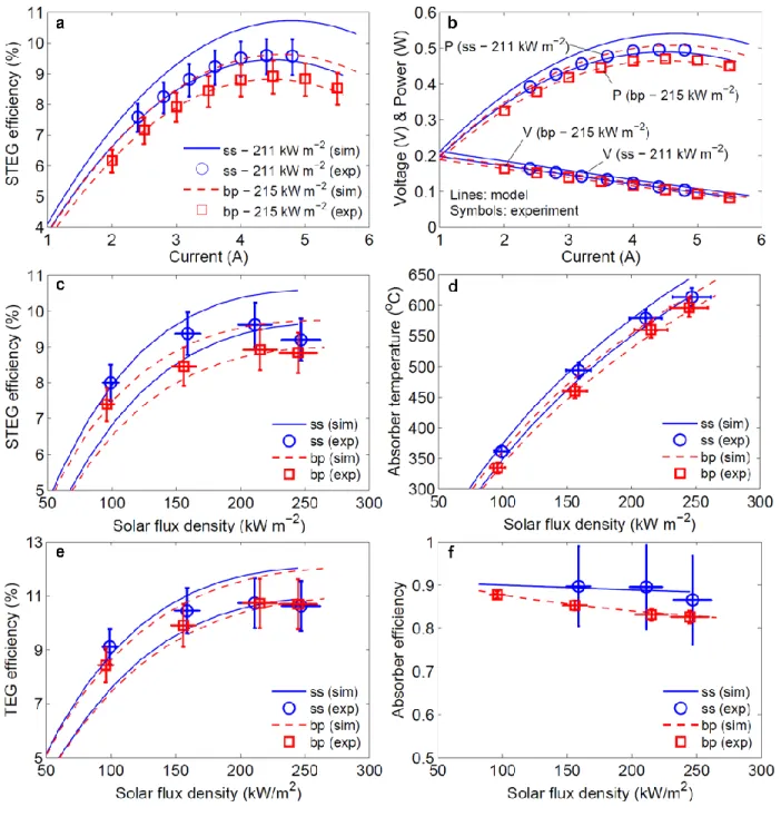
CSTEG Performance. Figures 2a and b show the performance of our fabricated STEGs
with spectrally-selective (ss) and black paint (bp) solar absorbers as a function of thermoelectric current at solar irradiances of 211 kW m-2 and 215 kW m-2, respectively, for the device with high optical solar concentration (Copt ≈ 200, Cth = 1.4, CCR ≈ 280). The STEG with the spectrally-selective solar absorber peaks at a record-high efficiency of 9.6%, which is almost 3 times more efficient than Telkes’ best device and twice as efficient as our previous work (Fig. 2a).7,9 As expected from Eq. (2), at high solar irradiances the STEG with the black paint solar absorber performs with a similar peak efficiency of 8.9% because the high optical concentration effectively reduces radiation heat loss. The STEG power output reaches 0.5 W (Fig. 2b) corresponding to a power output density of ~30 kW m-2 based on the cross-sectional area of the single couple TEG. At each solar irradiance set point the I-V curve measurement itself takes up
9
to two hours depending on the number of current set points to allow the STEG to reach its steady state at each current setting. No significant degradation of the STEG was observed in that time frame which is supported by the expected linear behavior of the I-V curves.
The STEG performances peak at solar irradiances of approximately 200 to 225 kW m-2 and the STEGs operate with an absorber temperature of approximately 560 to 580 °C (Fig. 2c and d) [see Methods for determination of absorber temperature]. For a decrease in the solar flux density by a factor of two we observe a drop in the STEG efficiency of approximately 17% which is smaller compared to what was previously observed for a purely thermally-concentrating STEG with a drop of approximately 25%.9 The operating temperature of the solar absorber
correspondingly falls to approximately 350 °C (Fig. 2d). The solar intensity varies over the course of a day. However, the tracking of the sun required for the concentrating optics leads to a reduction of this intensity variation.4 Nevertheless, CSTEGs with optical solar concentration should be optimized for maximum yearly energy output depending on its location and the level of optical concentration used.9,23 Concentrating optics cannot focus diffuse light, thus, CSTEGs perform best in locations with high DNI.
We further determined the TEG efficiency (ηteg) as a function of the solar irradiance close to 11% for the segmented TEG operating between 25 °C and approximately 570 °C (Fig. 2e) [see Methods Section]. This device efficiency corresponds to an effective ZT of ~0.64 which is significantly lower than the average material ZT of ~1.02 due to contact resistances, the infrared radiation losses from the thermoelectric legs and the radiative thermal shunting losses from the hot side to the cold side. Additionally, the uncertainties in the thermoelectric material properties might also contribute to the discrepancy in ZT. As expected, the determined absorber efficiency of approximately 90% for the spectrally-selective solar absorber (Fig.2f) is higher than that for
10
Figure 2 | Performance characteristics of a STEG optimized for high optical concentration.
Typical STEG performance characteristics at high solar flux densities and small thermal concentration ratio (Cth) of 1.4 with high-temperature spectrally-selective (ss) and black paint (bp) solar absorbers. Open squares and circles are experimental data, lines are modeling results of upper and lower bounds. (a) STEG efficiency versus electrical current of a STEG with ss at 211 kW m-2 and bp at 215 kW m-2 (b) I-V and I-P characteristics of a STEG with ss at 211 kW m-2 and bp at 215 kW m-2 (c) STEG efficiency, (d) absorber temperature, (e) TEG efficiency and (f) absorber efficiency as a function of incident solar flux density. Error bars in all subfigures are the result of uncertainty in incident radiation power measurement.
11
the black paint solar absorber. The discrepancy between experiment and modeling is larger at higher solar irradiances because the rising absorber temperature due to the fixed STEG geometry results in a disproportional increase of the infrared radiation heat loss which is more pronounced for the black paint compared to the low-emittance selective solar absorber. Another possible explanation is absorber damage since at ~250 kW m-2, the absorber operating temperature is above 600 oC (Fig.2d) while the double-cermet absorber was only proven to be stable in vacuum up to 600 °C.41 Overall, however, the gain in efficiency by using a spectrally-selective solar absorber instead of black paint at such high optical solar concentration is not substantial and might not justify the increased complexity in the STEG fabrication.
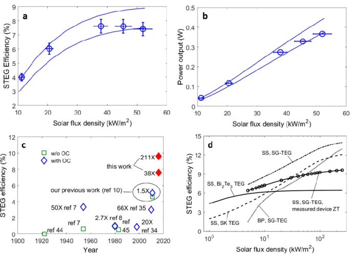
Figure 3 shows the results of a STEG optimized for moderate optical concentration (Copt ≈ 50, Cth = 5.4, CCR ≈ 270). The larger thermal radiation heat loss of the solar absorber limits the peak STEG efficiency to 7.6% and the peak power output to close to 0.3 W at a solar irradiance of ~38 kW m-2 (Fig. 3a and b). The absorber operating temperature at peak STEG performance is approximately 420°C. Even though the performance is worse compared to STEGs optimized for high optical solar concentration, it is still a remarkable improvement over previous reports in the literature (Fig. 3c).7,9,10,35,37,38,43,44 All reported STEG efficiencies in Fig.3c are based on the solar radiation power incident on the solar absorber, thus, excluding the optical losses from concentrating optics. The record-high STEG efficiencies demonstrated here at moderate and high solar irradiances of ~38 kW m-2 and ~210 kW m-2 are still ~2–3 times higher compared to previously-reported best values for CSTEGs with similar optical solar concentrations.7,38
System Efficiency and Directions for Improvement. Our CSTEG experiments are
12
Figure 3 | Performance characteristics of a STEG optimized for moderate optical
concentration. Typical STEG performance characteristics at moderate solar flux densities and
thermal concentration ratio (Copt ≈ 50, Cth = 5.4, CCR ≈ 270) with a high-temperature spectrally-selective solar absorber. Open circles are experimental data, lines are modeling results of upper and lower bounds. (a) STEG efficiency (at peak efficiency under 38 kW/m2 illumination, absorber temperature is 420 oC) and (b) STEG output power. Error bars are the result of uncertainty in incident radiation power measurement. (c) Historical overview of experimental efficiency demonstrations of STEGs with (diamond symbol) and without (square symbol) optical concentration (OC). STEG efficiencies are based on the solar radiation flux incident on the solar absorber excluding optical losses from concentrating optics. (d) Simulated maximum efficiencies of STEGs with various design configurations optimized over a range of solar flux densities: STEG with spectrally-selective (SS) solar absorber and a TEG based on bismuth telluride (Bi2Te3) (solid line), skutterudite (SK, dashed line), segmented (SG, Bi2Te3+skutterudite) legs (dash-dotted line) and a TEG based on our measured effective device ZT (solid line with open circles); STEG with back paint (BP) absorber and segmented TEG (dotted line).
13
and the solar radiation from the solar simulator is focused with an uncoated N-BK lens (solar transmittance of ~0.92) onto the STEG test assembly (Supplementary Fig. 9). Taking into account these optical losses and assuming a diffuse light fraction of 10% the highest demonstrated CSTEG efficiencies are ~7.4% and ~5.9% at high and moderate optical solar concentration, respectively. The performance improvements of our STEGs compared to previous works can mainly be attributed to the use of segmented thermoelectric legs consisting of low-temperature bismuth telluride and temperature skutterudite materials, a
high-temperature spectrally-selective solar absorber and a vacuum environment (Fig. 3d). These three key design features enable a stable and efficient STEG operation with much larger operating temperature differences. The vacuum environment is essential not only for reducing heat losses but also for the high-temperature stability of the fabricated STEGs. The thermoelectric materials and the spectrally-selective solar absorber oxidize in air at high temperatures, detrimentally affecting their properties and the STEG performance.
Figure 3d illustrates theoretical calculations of various STEG configurations under vacuum for a range of incident solar flux densities. The calculations use the typical properties of the developed spectrally-selective solar absorber, bismuth telluride and skutterudite materials (Supplementary Fig. 1). The calculations do not take into account radiation losses from the thermoelectric legs and assume negligible contact resistances. Similar to most experimental efforts reported in literature, a STEG based on a low-temperature material such as bismuth telluride (Bi2Te3) is significantly limited in its efficiency due to the material’s maximum operating temperature of ~250 °C (Fig. 3d: solid line). High-temperature thermoelectric materials such as skutterudite enable operation with much larger temperature differences (Fig. 3d: dashed line). This can significantly increase the maximum achievable STEG
14
efficiency, despite the poor TEG performance at low temperatures. A STEG with segmented thermoelectric legs consisting of bismuth telluride as the low-temperature and skutterudite as the high-temperature section can exploit a large temperature difference more efficiently to further improve the STEG performance (Fig. 3d: dash-dotted line). The use of a spectrally-selective instead of a black paint solar absorber can boost the STEG efficiency especially of STEGs optimized for low and moderate optical solar concentrations (Fig. 3d: dash-dotted and dotted lines). Figure 3d also illustrates the simulated STEG performance using the effective device ZT (solid line with open circles) that is obtained from our demonstrated TEG efficiencies (Fig. 2e). This effective device ZT is substantially lower compared to the average materials ZT due to experimental imperfections such as electrical contact resistances and radiation heat losses. Thus, our lab scale device tests demonstrate a lower STEG performance than theoretically is
achievable. This highlights the challenges and importance of thermoelectric device
demonstrations in addition to materials development and properties measurements. Furthermore, the discrepancy between our experiments and the theoretical predictions of ~14% (Fig. 3d) suggests substantial room for further improvement in the efficiency of current STEGs by reducing the effects of electrical contact resistance and radiation heat losses. The negative impacts of contact resistance can be overcome by identifying better contacts or increasing the lengths of the thermoelectric legs; and radiation heat can be minimized by increasing the cross-sectional area to reduce relative radiation heat loss from side walls, or placing multiple legs close to each other.
The large CCR of up to 295X, achieved by combining optical and thermal concentration, enable our CSTEGs to generate an electrical peak power output of up to ~0.5 W with only ~0.9 gram of thermoelectric material (Fig. 2b and 3b). At the current prices of the used bismuth
15
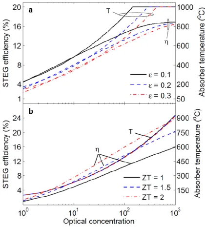
telluride and skutterudite based materials, the cost for the TEG’s thermoelectric material is approximately $26 per kg or $0.046 per electrical peak watt generated (Supplementary Table 2). Although the device fabrication will certainly increase the cost beyond just materials cost, the low material cost is a good starting point. The amount of thermoelectric material can further be reduced without significantly affecting the STEG performance as long as the electrical contact resistance is small.23 It should be acknowledged that our demonstrated peak TEG efficiency of about 11% is 3-4 times lower than the efficiencies of currently used mechanical heat engines.45 Consequently, at the current state the demonstrated STEG is not yet competitive economically. However, TEGs with higher efficiencies have been reported.31,33 Additionally, there are several avenues to further improve the STEG performance: (1) increasing optical solar concentration which increases both abs and teg, (2) reducing the infrared emittance of the solar absorber, (3) improving thermoelectric materials, and (4) improving device design to minimize radiation losses from side walls of thermoelectric legs and from the back side and edges of the solar absorber. Figure 4a shows the predicted maximum efficiencies as a function of optical solar concentration for a STEG with an effective device ZT of 1 and based on a solar absorber with solar absorptance of 0.93 and several effective infrared emittance values. With a solar absorber temperature limited to 1000 °C a STEG can reach an efficiency of over 16% at optical solar concentration of 1000X. At such high optical concentration the infrared emittance of the solar absorber does not significantly affect the performance of the STEG despite the high operating temperature. Thus, the selective solar absorber can be replaced with a high-temperature stable black solar absorber/receiver which eliminates the challenge of developing a thermally stable selective solar absorber. Figure 4b shows the predicted maximum efficiencies as a function of optical solar concentration of a STEG based on a blackbody solar absorber for different effective
16
device ZTs. With an absorber temperature reaching close to 1000 °C and thermoelectric materials with an effective ZT of 2 the maximum STEG efficiency can reach close to 24%. However, operating a STEG with such a large operating temperature difference requires TEGs with thermoelectric materials that can operate efficiently at temperatures up to 1000 °C. Recent progress made in high-temperature thermoelectric materials and device demonstrations raises hope of achieving predicted efficiencies.19,31,33 One of the main advantages of CSP is
dispatchability by using inexpensive thermal storage. Solar CSTEG can also be coupled to a
Figure 4 | Theoretical predictions of STEG efficiencies and corresponding optimal solar absorber temperatures. STEG efficiencies and optimal absorber temperatures are calculated as
a function of optical concentration based on the solar radiation flux incident on the solar absorber. Solar absorber temperature is limited to 1000 °C and the cold-side temperature is 50 °C. (a) Simulated performance of a STEG with an effective ZT = 1 thermoelectric material and selective absorber with solar absorptance of 0.93 and IR emittance (ε) of 0.1, 0.2 and 0.3. (b)
17
STEG with a blackbody solar absorber (solar absorptance and IR emittance of 1) and thermoelectric material with effective ZT of 1, 1.5 and 2.
thermal storage system, although the device and system configurations would need to be
redesigned. Thus, future research should not only focus on improving the CSTEG efficiency but also on the incorporation of thermal storage. Our experimental results should stimulate such research.
Methods
Device Modeling and Optimization. The optimum design of CSTEGs depends on the
incident solar radiation power, the solar absorber properties, the emittance values of surfaces participating in the CSTEG’s radiative heat transfer with the surroundings, the thermoelectric material properties, the cold-side temperature, and the device geometry (Supplementary Fig. 2). The lengths of the bismuth telluride and skutterudite sections are optimized for highest
segmented thermoelectric leg efficiency and the cross-sectional areas are optimized for highest TEG efficiency using a numerical solver based on the iterative method and the Domenicali’s equations modified to include leg radiation losses, keeping in mind of the limits of the maximum current can be supplied by our instruments (Supplementary Method S1).11,23,46 For the given TEG geometry and with its calculated performance characteristics as a function of hot-junction temperature, the area of the solar absorber with known temperature-dependent properties is optimized to find the optimal thermal concentration for moderate and high incident solar radiation power densities.
The upper and lower bounds in Fig. 2 are calculated with the uncertainties in thermoelectric material properties and uncertainties in the optical properties of surfaces which participate in the radiation heat transfer affecting the STEG performance. We also take into account results from a TEG characterization experiment that shows the Seebeck voltage to be ~5% lower and the
18
electrical resistance to be ~12% higher than expected for our fabricated TEGs (Supplementary Method S3).
Device Fabrication. Details about the fabrication and properties of the used thermoelectric
elements and solar absorbers as well as the fabrication and testing of the CSTEG assemblies are given in Supplementary Methods S2 and S3 and briefly summarized here. The individual thermoelectric elements (bismuth telluride and skutterudite) are fabricated with hot-pressed contact pads using a ball mill and a subsequent hot-press process (Supplementary Fig. 3).30,32,47 The segmented legs are fabricated by soldering the bismuth telluride and skutterudite elements to each other (Fig. 1b). The typical dimensions of the p-type segmented leg including contact pads is approximately 3 x 3 x 9 mm3 with the bismuth telluride and skutterudite sections being
1.75 mm and 5.9 mm long, respectively. The n-type segmented leg is of similar dimensions. A copper plate is brazed to the skutterudite ends as the hot junction electrically connecting the n/p-type segmented legs in series. The solar absorber is fabricated on a stainless steel substrate which is brazed to the hot-junction copper plate. Here, the hot-junction plate helps minimize temperature gradients within the solar absorber. The cold-junction copper electrodes for each of two bismuth-telluride legs are soldered onto individual thermoelectric coolers which are attached to a liquid-cooled stage for accurate and stable temperature control during the CSTEG device tests (Supplementary Fig. 6a). The segmented thermoelectric legs consisting of bismuth telluride and skutterudite materials are surrounded by tight copper radiation shields to reduce radiation heat loss.
The used spectrally-selective solar absorber is based on a double-cermet layer (W/Ni-filled Al2O3) deposited on a stainless steel substrate and is thermally stable in vacuum up to 600 °C (Supplementary Fig. 4).41 The solar absorber has a temperature-independent solar absorptance of
19
approximately 0.91 and measured infrared total hemispherical emittance of ~0.15 at 500 °C which can be extrapolated to ~0.18 at 600 °C. The high-temperature reference paint HE6 by Rolls Royce is applied on a stainless steel substrate and used as the black paint solar absorber with a temperature-independent solar absorptance and total-hemispherical emittance of 0.95 (Supplementary Fig. 6g).40,42
Device Testing. The STEG assembly is mounted onto a liquid cooled cold stage to minimize
thermal drift and tested inside a vacuum chamber with a fused silica viewport under concentrated solar radiation from a solar simulator (Fig. 1f). The vacuum levels during the CSTEG
experiments are maintained between 1⨯10-3 and 1⨯10-2 Pa. The measurement of the incident solar radiation power, Qabs, is performed before and after the CSTEG experiment using a
calibrated thermopile and power meter from Newport (Supplementary Method S3). The incident solar radiation power striking the solar absorber is accurately defined by a thermally grounded aperture placed in front of the solar absorber (Figs. 1c and 1e, Supplementary Fig. 6). The aperture opening has the same dimensions as and is aligned with the solar absorber.
A precision power supply and digital multimeter from Keithley is used to perform the current-voltage (I-V) curve measurements at constant solar radiation power striking the solar absorber (Qabs = Aabsqabs). The current voltage (I-V) curves (Fig. 2b) show the typical linear (resistive) behavior of a TEG with constant temperature difference,27 indicating that the decreasing absorber temperature due to the Peltier effect does not introduce a substantial nonlinearity in the I-V relation. From this data the peak STEG efficiency η = IV/Qabs can be found. This efficiency does not include the optical losses. The transmittance of the used
viewport and focusing lens is measured separately to estimate the optical losses (Supplementary Fig. 8).
20
In order to minimize heat losses, the solar absorber temperature is not measured in situ during the CSTEG experiments. Instead the fabricated STEGs are characterized in terms of their voltage output and electrical resistance as a function of hot-junction temperature by conducting a TEG characterization experiment (Supplementary Fig. 10). Using that information the absorber operating temperatures during the CSTEG experiment is measured using the TEG itself. With the measured STEG efficiency, the absorber temperature and the optical properties of the
reference black paint (HE6: αsol = ε = 0.95), the absorber and TEG efficiencies can be calculated as a function of solar radiation flux using Eq. (2) and Eq. (1), respectively (Figs.2e and 2f). More details are given in Supplementary Method S3.
References:
1. Jones-albertus, R., Feldman, D., Fu, R., Horowitz, K. & Woodhouse, M. Technology
Advances Needed for Photovoltaics to Achieve Widespread Grid Price Parity. (2015).
2. Luque, A. & Hegedus, S. Handbook of Photovoltaic Science and Engineering. (John Wiley & Sons, Inc., 2003).
3. Green, M. A. Third Generation Photovoltaics: Advanced Solar Energy Conversion. (Springer, 2003).
4. John A. Duffie, W. A. B. Solar Engineering of Thermal Processes. (2013).
5. Mills, D. Advances in solar thermal electricity technology. Sol. Energy 76, 19–31 (2004). 6. Weinstein, L. A. et al. Concentrating Solar Power. Chem. Rev. 115, 12797–12838 (2015). 7. Telkes, M. Solar Thermoelectric Generators. J. Appl. Phys. 25, 765–777 (1954).
8. Goldsmid, H. J. Applications of Thermoelectricity. (Methuen, 1960).
9. Kraemer, D. et al. High-performance flat-panel solar thermoelectric generators with high thermal concentration. Nat. Mater. 10, 532–8 (2011).
10. McEnaney, K., Kraemer, D. & Chen, G. Direct Heat-to-Electricity Conversion of Solar Energy. Annu. Rev. Heat Transf. 179–230 (2012).
doi:10.1615/AnnualRevHeatTransfer.2012004544
11. McEnaney, K., Kraemer, D., Ren, Z. & Chen, G. Modeling of concentrating solar thermoelectric generators. J. Appl. Phys. 110, 074502–8 (2011).
12. Venkatasubramanian, R., Siivola, E., Colpitts, T. & O’Quinn, B. Thin-film thermoelectric devices with high room-temperature figures of merit. Nature 413, 597–602 (2001).
21
13. Harman, T. C., Taylor, P. J., Walsh, M. P. & Laforge, B. E. Quantum Dot Superlattice Thermoelectric Materials and Devices. Science 297, 2229–2232 (2002).
14. Dresselhaus, M. S. et al. New Directions for Low-Dimensional Thermoelectric Materials.
Adv. Mater. 19, 1043–1053 (2007).
15. Poudel, B. et al. High-thermoelectric performance of nanostructured bismuth antimony telluride bulk alloys. Science (80-. ). 320, 634–638 (2008).
16. Heremans, J. P. et al. Enhancement of Thermoelectric Efficiency in PbTe by Distortion of the Electronic Density of States. Science 321, 1457–1461 (2008).
17. Snyder, G. J. & Toberer, E. S. Complex thermoelectric materials. Nat. Mater. 7, 105–14 (2008).
18. Biswas, K. et al. High-performance bulk thermoelectrics with all-scale hierarchical architectures. Nature 489, 414–8 (2012).
19. Zhao, L.-D. et al. Ultralow thermal conductivity and high thermoelectric figure of merit in SnSe crystals. Nature 508, 373–377 (2014).
20. Kim, S. I. et al. Dense dislocation arrays embedded in grain boundaries for high-performance bulk thermoelectrics. Science 348, 109–114 (2015).
21. Beekman, M., Morelli, D. T. & Nolas, G. S. Better thermoelectrics through glass-like crystals. Nat. Mater. 14, 1182–1185 (2015).
22. Zhao, L. et al. Ultrahigh power factor and thermoelectric performance in hole-doped single-crystal SnSe. Science (2015). doi:10.1126/science.aad3749
23. Kraemer, D., McEnaney, K., Chiesa, M. & Chen, G. Modeling and optimization of solar thermoelectric generators for terrestrial applications. Sol. Energy 86, 1338–1350 (2012). 24. Kim, H. S., Liu, W., Chen, G., Chu, C.-W. & Ren, Z. Relationship between thermoelectric
figure of merit and energy conversion efficiency. Proc. Natl. Acad. Sci. U. S. A. 112, 8205–10 (2015).
25. Snyder, G. J. Application of the compatibility factor to the design of segmented and cascaded thermoelectric generators. Appl. Phys. Lett. 84, 2436 (2004).
26. Ioffe, A. F. Semiconductor Thermoelements and thermo-electric cooling. (Infosearch Ltd, 1957).
27. Rowe, D. M. Thermoelectrics Handbook: Macro to Nano. (Taylor & Francis Group, LLC, 2006).
28. El-Genk, M. S., Saber, H. H., Sakamoto, J. & Caillat, T. Life Tests of a Skutterudites Thermoelectric Unicouple (MAR-03). in 22nd International Conference on
Thermoelectrics 417–420 (2003).
29. Guo, J. Q. et al. Development of Skutterudite Thermoelectric Materials and Modules. J.
Electron. Mater. 41, 1036–1042 (2012).
30. Muto, A., Yang, J., Poudel, B., Ren, Z. & Chen, G. Skutterudite Unicouple
Characterization for Energy Harvesting Applications. Adv. Energy Mater. 3, 245–251 (2013).
22
Thermoelectric Couples. Nucl. Emerg. Technol. Sp. (2012).
32. Kraemer, D. et al. High thermoelectric conversion efficiency of MgAgSb-based material with hot-pressed contacts. Energy Environ. Sci. 8, 1299–1308 (2015).
33. Cook, B. A. et al. High-Performance Three-Stage Cascade Thermoelectric Devices with 20% Efficiency. J. Electron. Mater. 44, 1936–1942 (2015).
34. Salvador, J. R. et al. Conversion efficiency of skutterudite-based thermoelectric modules.
Phys. Chem. Chem. Phys. 16, 12510–20 (2014).
35. Goldsmid, H. J., Giutronich, J. E. & Kaila, M. M. Solar thermoelectric generation using bismuth telluride alloys. Sol. Energy 24, 435–440 (1980).
36. Dent, C. L. & Cobble, M. H. A solar thermoelectric generator experiments and analysis. in
4th International Conference on Thermoelectric Energy Conversion 75–78 (1982).
37. Omer, S. Design optimization of thermoelectric devices for solar power generation. Sol.
Energy Mater. Sol. Cells 53, 67–82 (1998).
38. Amatya, R. & Ram, R. J. Solar Thermoelectric Generator for Micropower Applications. J.
Electron. Mater. 39, 1735–1740 (2010).
39. Baranowski, L. L., Snyder, G. J. & Toberer, E. S. Concentrated solar thermoelectric generators. Energy Environ. Sci. 5, 9055–9067 (2012).
40. Kraemer, D., McEnaney, K., Cao, F., Ren, Z. & Chen, G. Accurate determination of the total hemispherical emittance and solar absorptance of opaque surfaces at elevated temperatures. Sol. Energy Mater. Sol. Cells 132, 640–649 (2015).
41. Cao, F. et al. Enhanced Thermal Stability of W-Ni-Al 2 O 3 Cermet-Based Spectrally Selective Solar Absorbers with Tungsten Infrared Reflectors. Adv. Energy Mater. 5, 1401042 (2015).
42. Brandt, R., Bird, C. & Neuer, G. Emissivity reference paints for high temperature applications. Measurement 41, 731–736 (2008).
43. Coblentz, W. W. Harnessing heat from the sun. Sci. Am. 127, 324 (1922).
44. Durst, T., Harris, L. B. & Goldsmid, H. J. Studies of a thermoelectric generator from tubular solar collectors. Sol. Energy 31, 421–425 (1983).
45. NREL. Concentrating Solar Power Research. (2012).
46. Domenicali, C. A. Irreversible Thermodynamics of Thermoelectric Effects in Inhomogeneous, Anisotropic Media. Phys. Rev. 92, 877–881 (1953).
47. Liu, W. et al. Understanding of the contact of nanostructured thermoelectric n-type
Bi2Te2.7Se0.3 legs for power generation applications. J. Mater. Chem. A 1, 13093–13100 (2013).
23
Acknowledgments: This material is partially based upon work supported as part of the Sunshot
Initiative funded by the U.S. Department of Energy, Office of Energy Efficiency & Renewable Energy under Award Number: DE-EE0005806 (for device engineering) and based upon work supported as part of the Solid State Solar-Thermal Energy Conversion Center (S3TEC), an Energy Frontier Research Center funded by the U.S. Department of Energy, Office of Science, Office of Basic Energy Sciences under Award Number:DE-SC0001299/DE-FG02-09ER46577 (for materials)
Authors contributions: D.K. carried out modeling and simulation, CSTEG fabrication and
experiments, and prepared the manuscript; Q.J. and W.S.L. fabricated the thermoelectric and contact materials; K. M. contributed to CSTEG fabrication and experiments and device modeling; F.C. fabricated spectrally-selective solar absorbers; L.W. contributed to manuscript preparation and CSTEG fabrication and experiments; J.L. contributed to CSTEG fabrication and experiments; Z.F.R. directed research at UH; G.C. directed research at MIT and contributed to the manuscript preparation.
Supporting Online Material for
High performance cC
oncentrating solar thermoelectric generators
with a
peak efficiency of 7.4%
Daniel Kraemer, Qing Jie, Kenneth McEnaney, Feng Cao, Weishu Liu, Lee A. Weinstein, James Loomis, Zhifeng Ren,* and Gang Chen*
*Corresponding authors: gchen2@mit.edu, zren@uh.edu
This supplement contains
Supplementary Figures S1-S10 Supplementary Tables S1 and S2 Supplementary Modeling Methods 1-3
Experimental details: materials, device fabrication and device testing Supplementary References
Supplementary Figure S1| Typical material properties of hot-pressed thermoelectric legs
measured with commercial equipment (ZEM 3 and Laser Flash method): p-type Bi0.4Sb1.6Te3-Sb0.01, n-type Bi2Te2.7Se0.3+S0.015, p-type Ce0.45Nd0.45Fe3.5Co0.5Sb12, n-type
Ba0.08La0.05Yb0.04Co4Sb12.
Supplementary Figure S2| CSTEG schematic illustrating heat flows.
Supplementary Figure S3| Illustration of layers in individual thermoelectric (TE) legs, which
are hot-pressed together with the optimal contact pad material, and photographs of individual legs. To minimize elemental sublimation in vacuum at high temperatures the skutterudite legs are coated with 1 µm Al2O3. For more reliable brazing and soldering processes the contact ends are electroplated with copper, nickel and gold.
Supplementary Figure S4| Vacuum brazing process for hot-junction brazed joints and for
brazing the stainless steel (SS) absorber substrate to the hot-junction copper plate. (a) Braze assembly: Braze copper enclosure (also shown in (b)) is heated with an electrical heater. Thin-film braze
(Ag56Cu22Sn5Zn17, Ts/l = 618/650 ˚C) is sandwiched between the skutterudite (SKU) legs and the copper (Cu) hot-junction plate and the Cu plate and the SS absorber substrate. The pieces are held in place and pushed onto an electrical ceramic heater by 2 spring-loaded pins.
Temperatures of heated braze copper enclosure and the bottom ceramic heater are measured with thermocouples (TC). (c) and (d) Finished SS-Cu-SKU brazed joints.
Supplementary Figure S5| High-temperature spectrally-selective solar absorber of STEG
assembly. (a) Al2O3cermet-based coating is deposited onto the polished stainless steel absorber substrate after the hot-junction brazing step. (b) – (c) Material properties of solar absorber coating.
Supplementary Figure S6| Vacuum soldering process for final STEG fabrication steps. (a)
Vacuum soldering setup is the same as the vacuum brazing setup (figure S4(a)). Thin-film solder (Pb90Sb10, 252/260 ˚C) is sandwiched between the skutterudite and Bi2Te3 legs and between the Bi2Te3 and the cold-junction copper electrodes. STEG assembly is held in place and pressed onto a ceramic heater with 2 spring-loaded pins. (b) Fabricated STEG assembly. (c) Fabricated STEG assembly with TE leg radiation shield soldered to the copper electrodes with 138 ˚C solder.
Supplementary Figure S7| STEG test setup. (a) STEG is soldered (120 ˚C solder) with its
cold-junction copper electrodes onto 2 thermoelectric cooler (TEC) modules enabling accurate cold-junction temperature control. The TECs are soldered onto a liquid-cooled copper cold stage. (b) The STEG is surrounded by the aperture plate holder which is thermally grounded to the cold stage. (c) A solar absorber edge radiation shield closely surrounding the solar absorber (e) is bolted to the aperture holder. (d) The aperture plate is bolted on top of the edge radiation shield plate. (f) The aperture is aligned with the solar absorber of same dimensions. (g) The STEG is also tested with a black paint solar absorber by coating the selective surface with a reference black paint (HE6).
Supplementary Figure S8| STEG test rig for horizontal solar simulator beam path. (a) STEG
assembly is mounted onto the liquid-cooled copper cold stage. The aperture copper plate is spray-coated with boron nitride. (b) The liquid-cooled cold stage with the STEG test setup is mounted vertically inside a vacuum chamber.
Supplementary Figure S9| Incident power measurement. (a) The radiation coming from the
solar simulator transmits through an AM1.5G filter, the fused silica viewport of the vacuum chamber and strikes the test rig. (b) In order to measure the solar radiation passing through the aperture of the STEG assembly, the STEG is removed allowing the solar radiation passing through the aperture to strike a thermopile radiation detector. (c) Measured spectral transmission of the used fused silica viewport and N-BK lens. This spectral data is used to calculate the optical losses and optical efficiency of the experiment.
Supplementary Figure S10| TEG characterization. (a) An electrical heater embedded in a
copper enclosure is brazed to the STEG’s solar absorber and surrounded by a heated radiation shield (b) to reduce the required electrical power input. (c) The experimentally measured open circuit voltage (markers) as a function of hot-junction temperature of the TEG is in good
agreement with calculation results (line) by adding a thermal contact resistance of 5 %. (d) The electrical resistance calculations can be matched with the experiments by introducing a
temperatureindependent total electrical contact resistance of 2.3 mΩ.
Supplementary Table S1| Details about used thermoelectric legs.
thermoelectric leg
thermoelectric material contact pad material + thickness hot-press temperature dimensions WxDxL (mm3) p-type Skutterudite Ce0.45Nd0.45Fe3.5Co0.5Sb12 Fe-based alloy ~0.29 mm 700 ˚C 3.03x3.00x5.91 n-type Skutterudite Ba0.08La0.05Yb0.04Co4Sb12 CoSi2 ~0.57 mm 800 ˚C 2.73x2.73x6.27 p-type Bi2Te3 Bi0.4Sb1.6Te3-Sb0.01 Ni ~0.36 mm 500 ˚C 2.95x2.93x1.75 n-type Bi2Te3 Bi2Te2.7Se0.3+S0.015 NiInFeS ~0.32 mm 525 ˚C 2.61x2.68x1.47
Supplementary Table S2| Thermoelectric bulk material cost analysis.
Supplementary Methods
S1.Supplementary Method 1 | Modeling
Our modeling approach has been described in detail in multiple previous publications.1,2,3,4 We only give a short summary here.
S1.1 Thermoelectric couple modeling
First, the performance characteristics (efficiency, hot-junction heat input, electrical power output, etc.) of the individual segmented thermoelectric legs are calculated using the
temperature-dependent properties of the thermoelectric materials (supplementary figure S1) and Domenicali’s coupled 1st order equations which are modified to include the effect of leg
radiation heat loss.4,5
𝑑𝑇 𝑑𝑥 = 𝑖(𝑆𝑇)𝑥− 𝑞𝑙𝑒𝑔(𝑥) 𝑘(𝑥) (S1) 𝑑𝑞𝑙𝑒𝑔 𝑑𝑥 = [𝑖𝜌(𝑥) + 𝑆(𝑥) 𝑖(𝑆𝑇)𝑥− 𝑞𝑙𝑒𝑔(𝑥) 𝑘(𝑥) ] 𝑖 − P𝑞𝑟𝑎𝑑(𝑥) 𝐴𝑙𝑒𝑔 (S2)
Those coupled first-order equations are solved iteratively for the n- and p-type elements for the optimal thermoelectric heat flux and temperature distribution corresponding to the optimum current densities for a specified TEG geometry (lengths and cross-sectional areas of
thermoelectric elements). Equation (S1) correlates the local temperature gradient dT(x)/dx to the local heat flow density, qleg(x), the current density i = I/Aleg with I and Aleg being the applied
current and the cross-sectional area of the thermoelectric leg, respectively, the local thermal conductivity, k(x), and Seebeck coefficient, S(x) due to their dependence on local temperature
T(x). Equation (S2)(S2) correlates the local change in the heat flow density, dqleg(x)/dx with the
local electrical resistivity ρ(x). The last term on the right hand side of equation (S2) appears due to the radiative heat transfer between the thermoelectric leg and the surroundings with P being the leg perimeter. In the case of a TEG with two closely-spaced thermoelectric legs we assume negligible radiation heat loss from the side walls facing each other. Thus, only 3 side-walls of the thermoelectric leg contribute to the radiative heat transfer with the surroundings. The local leg radiation power density can be defined as qrad = εeff(T(x))σ(T(x)4-Tc4) with εeff being the
effective leg IR emittance, σ the Stefan-Boltzmann constant and Tc being the surrounding
cold-side temperature. For dx → 0 the equations (S3) and (S4)(S2) can be written for the ith segment as:
𝑇𝑗+1 = 𝑇𝑗+𝑑𝑥
𝑞𝑗+1 = 𝑞𝑗+ [𝑞𝑗𝑖2(1 +𝑆𝑗 2𝑇 𝑗 𝜌𝑗𝑘𝑗) − 𝑖𝑆𝑗𝑞𝑗 𝑘𝑗 − 3𝑞𝑟𝑎𝑑,𝑗 𝐴𝑙𝑒𝑔 ] 𝑑𝑥, (𝑗 = 0, 1, 2, … , 𝑛 − 1) (S4)
The output from one segment of the leg becomes the input for the adjacent segment, such that the iterative method6 can be used to accurately determine the temperature and heat flow profile of the thermoelectric leg for each applied electrical current with TCJ and THJ as the specified cold and hot
junction temperature boundary conditions. From that the heat flow at the hot junction, 𝑄𝑙𝑒𝑔,𝐻𝐽 = 𝑞𝑙𝑒𝑔,𝑛∙ 𝐴𝑙𝑒𝑔, the created thermoelectric leg voltage, 𝑉𝑙𝑒𝑔 = ∑𝑛−10 𝑆𝑗(𝑇𝑗+1− 𝑇𝑗)+ 𝑖 ∑𝑛−10 𝜌𝑗𝑑𝑥, the thermoelectric leg power output, 𝑃𝑙𝑒𝑔= 𝑉𝑙𝑒𝑔𝐼, and leg conversion efficiency, 𝜂𝑙𝑒𝑔 = 𝑃𝑙𝑒𝑔
𝑄𝑙𝑒𝑔 at every given electrical current is determined. It shall be noted that for the defined x direction the current and heat flow densities are negative for a p-type thermoelectric leg.
The optimization is performed for both thermoelectric legs with the same length. Due to the difference in the n- and p-type thermoelectric material properties, the cross-sectional area of the thermoelectric elements are different and the cross-sectional area ratio must be optimized using the iteration process. The boundary conditions for the differential equations of both
thermoelectric elements are the same fixed cold- and hot-junction temperatures that uniquely determine the optimal current, the temperature and heat flux distribution for the specified single-couple TEG geometry. The thermoelectric efficiency can be calculated with 𝜂𝑡𝑒= 𝑄𝑡𝑒𝑃𝑡𝑒=
𝐼(𝑉𝑙𝑒𝑔,𝑝+𝑉𝑙𝑒𝑔,𝑛)
𝑄𝑙𝑒𝑔,𝑝+𝑄𝑙𝑒𝑔,𝑛 . Electrical contact resistances can easily be included in the calculations by adding segments with corresponding electrical resistivity and a negligible Seebeck coefficient to the hot and cold end of the thermoelectric elements.
S1.2 CSTEG modeling
The CSTEG test devices consist of one thermoelectric couple sandwiched between the solar absorber and a heat sink (supplementary figure S2). Knowing the heat flow into the
thermoelectric couple, Qte, the energy balance for the solar absorber with negligible temperature
gradients yields
𝑄𝑡𝑒𝑔 = 𝑄𝑡𝑒+ 𝑄𝑠ℎ = 𝛼𝑠𝑜𝑙𝐴𝑎𝑏𝑠𝑞𝑎𝑏𝑠− 𝐴𝑎𝑏𝑠𝜀(𝑇𝑎𝑏𝑠)𝜎(𝑇𝑎𝑏𝑠4 − 𝑇𝑎𝑚𝑏4 ) (S5)
with Qteg being the hot-side heat input power to the TEG determined by the heat flow into the
thermoelectric couple and possible thermal radiation shunting heat loss, Qsh, from the edges and
the back side of the solar absorber to the surroundings. The heat flow, Qteg, at a given CSTEG
operating temperature difference must be balanced in steady state by the absorbed solar radiation (first term on the right hand side of S5) and the radiation heat loss from the solar absorber
surface (second term on the right hand side). The absorbed solar radiation is dependent on the solar absorptance, αsol, the absorber area, Aabs, and the incident absorber solar radiation flux
density, qabs = ηoptCoptqsol determined by the optical efficiency, the optical solar concentration
and the solar intensity striking the concentrating optics. The infrared radiation heat loss from the solar absorber surface is determined by its total-hemispherical emittance, ε(Tabs), and operating
temperature, Tabs, and surrounding temperature, Tamb. The assumption of a uniform solar
discussed in great detail in one of our previous publications.4 One of our design solutions to address the challenge of efficient thermal concentration is to use a thick hot-junction copper plate with the same area as the stainless steel substrate of the solar absorber. This allows the absorbed solar radiation to be conducted to the thermoelectric legs with negligible temperature gradients. From the correlation (S5) the absorber efficiency can be obtained as
𝜂𝑎𝑏𝑠 = 𝑄𝑡𝑒𝑔
𝐴𝑎𝑏𝑠𝑞𝑎𝑏𝑠 = 𝛼𝑠𝑜𝑙−
𝜀(𝑇𝑎𝑏𝑠)𝜎(𝑇𝑎𝑏𝑠4 − 𝑇𝑎𝑚𝑏4 )
𝜂𝑜𝑝𝑡𝐶𝑜𝑝𝑡𝑞𝑠𝑜𝑙 (S6)
The TEG efficiency includes the possible thermal shunting losses, Qsh, and can be expressed as
𝜂𝑡𝑒𝑔 = 𝐼(𝑉𝑙𝑒𝑔,𝑝+ 𝑉𝑙𝑒𝑔,𝑛) 𝑄𝑡𝑒+ 𝑄𝑠ℎ =
𝑃𝑡𝑒
𝑄𝑡𝑒𝑔 (S7)
Therefore, the CSTEG efficiency can be calculated with a given optical efficiency, ηopt, for the
concentrating optics with 𝜂 = 𝑞𝑎𝑏𝑠 𝐶𝑜𝑝𝑡𝑞𝑠𝑜𝑙 (𝑞𝑡𝑒+ (𝐶𝑡ℎ− 1)𝑞𝑏+ 𝐴𝑒 𝐴𝑡𝑒 ⁄ 𝑞𝑒) 𝐶𝑡ℎ𝑞𝑎𝑏𝑠 𝑃𝑡𝑒 𝑄𝑡𝑒𝑔= 𝜂𝑜𝑝𝑡𝜂𝑎𝑏𝑠𝜂𝑡𝑒𝑔 (S8)
where Copt is the optical concentration (area ratio), qsol the solar intensity, qabs the solar flux
density incident on the solar absorber, qte the hot-junction heat flux density of the thermoelectric
couple, qb and qe the thermal radiative heat flux densities of the back side and edges of the solar
absorber, respectively, with Ae being the edge area and Cth = Aabs/Ate being the thermal
concentration ratio defined as the ratio of the solar absorber area to the cross-sectional area of the thermoelectric couple.
To simulate the experimental results, the temperature-dependent properties of the p-type and n-type elements as shown in supplementary figure S1 and their typical dimensions as shown in supplementary table S1 were used. We modify the Seebeck coefficient and electrical resistance of the thermoelectric couple according to measured results from the TEG characterization experiment which is discussed later. For the optical properties of the solar absorber we use the typical measured solar absorptance and temperature-dependent total hemispherical emittance of the selective absorbers as shown in supplementary figure S5. The emittance values and their temperature dependence of the thermoelectric legs and the back side and edges of the solar absorber are less accurately known. Hence, these emittance values are treated as fitting parameters. Values obtained, however, are within reason.
Supplementary Method 2 |S2. Fabrication of STEG Assembly
The fabrication of a STEG cell for proof of concept testing is not a straightforward task and the process required careful optimization. In addition to the fabrication and optimization of the individual thermoelectric elements (including contact pad materials) the main challenge of the
STEG cell fabrication is joining 4 individual thermoelectric legs to a mechanically strong segmented-leg single-couple TEG with reasonably low contact resistances without negatively affecting their material properties. Furthermore, a high-temperature solar absorber needs to be attached to the hot junction of the single-couple TEG with minimal thermal resistance and without damaging the absorber surface. The optimized fabrication process is described in the following sections.
S2.1 Preparation of thermoelectric legs
The thermoelectric material is ball-milled and hot-pressed together with the contact pad material to a sample disc equivalent to the process described in previous publications.7 The hot-press temperatures are given in supplementary table S1. Each thermoelectric disc is hot-pressed to the optimal thickness obtained by the single segmented TE leg solver (modeling section) that
optimizes the leg lengths of the Bi2Te3 and the skutterudite leg section for maximum segmented TE leg efficiency while maintaining the total length of the segmented leg constant. The
thermoelectric discs are then cut to individual TE legs with optimal cross-sectional areas leading to maximum single-couple TEG efficiency. The geometry optimization of the segmented TE legs is performed with typical material properties of the fabricated TE materials as shown in supplementary figure S1.
For a successful lab-scale device test the cross-sectional area of the TE legs should be large while the length of the segmented TE legs should be minimized in order to minimize the effect of leg radiation as long as the electrical contact resistances are negligible. However, there are two experimental limitations that put constraints on the TE leg dimensions. (1) The minimum TE disc thickness is approximately 1.5 mm for the used hot-press process. This sets the minimum segmented TE leg length. (2) The maximum cross-sectional areas of the TE legs are determined by the maximum solar radiation power and/or maximum electrical current that can be supplied to the CSTEG by the solar simulator and power supply, respectively. Details about the fabricated TE legs including typical dimensions used in the experiments are shown in table S1.
Further preparation of the TE legs is required before they can be assembled into a segmented-leg single-couple TEG. The final TE legs are shown in supplementary figure S3. The skutterudite legs are coated with a 1 μm thick Al2O3 film to minimize sublimation of elements with high vapor pressures such as antimony during the high-temperature vacuum brazing process. The end surfaces of the contact pads are polished, cleaned and electroplated with copper, nickel and gold for more reliable brazing and soldering processes.
S2.2 High-temperature vacuum brazing process
A high-temperature vacuum brazing process (supplementary figure S4) is developed to join the p- and n-type skutterudite legs with a copper hot-junction plate using a silver-based thin foil braze (Ag56Cu22Sn5Zn17, solidus/liquidus = 618/650 ˚C). Additionally, the stainless steel solar absorber substrate is simultaneously brazed to the hot-junction copper plate with the same type of thin foil braze to ensure excellent mechanical and thermal contact between the solar absorber and the hot-junction of the single-couple TEG. It is important that the spectrally-selective surface of the solar absorber is deposited on the stainless steel substrate after the
high-temperature brazing step to avoid affecting its optical properties. There are several reasons for performing the brazing process in a vacuum. (1) No oxidation of surfaces during the high-temperature brazing. (2) If the contact surfaces are not oxidized and are clean, there is no braze flux required as the latter can damage and/or contaminate the thermoelectric material and is difficult to remove without leaving residue on the CSTEG’s surfaces. Thus, (3) it is a clean brazing process which leads to minimal increase in IR emittance of the CSTEG’s surfaces. (4) It is a controlled brazing process in terms of brazing temperature, time and environment which is especially important because the brazing temperatures are close to the skutterudite hot-pressing temperatures (table S1).
Supplementary Figures S4(a) and (b) show the brazing setup. It consists of a copper enclosure heated by a ceramic heater and a second bottom heater which can quickly change temperature by adjusting its electrical power input. The skutterudite legs, the hot-junction copper plate and the stainless steel solar absorber substrate with thin-film braze in between the interface are held in place and pressed onto the bottom ceramic heater with 2 spring-loaded pins. The temperatures of the copper enclosure and the bottom ceramic heater are measured with thermocouples. Long term high-temperature exposure (>550 ˚C) of the skutterudite legs can affect their material properties and/or their interfaces with the contact pads. High temperatures close to the hot-press temperatures can promote accelerated sublimation of high vapor pressure elements, elemental diffusion between thermoelectric and contact pad materials and undesired annealing processes. For a good brazing joint, however, the brazing parts must be heated
uniformly to above the liquidus point of the braze of 650 ˚C. In order to minimize the time when the skutterudite legs are at temperatures above 550 ˚C, the copper enclosure is heated to 680 ˚C as quickly as possible. The bottom heater is thermally grounded to the liquid cooled cold stage which stays near room temperature. This causes the bottom heater and the skutterudite legs to lag behind in temperature by approximately 110 ˚C. As soon as the copper enclosure reaches 660 ˚C while the skutterudite legs only reach ~550 ˚C, the bottom heater is turned on to rapidly heat the brazing parts to above 680 ˚C. When the copper enclosure reaches 680 ˚C both ceramic heaters are turned off and the vacuum chamber is purged with argon gas for rapid cooling of the skutterudite legs to below 550 ˚C. This process limits the high-temperature exposure of the skutterudite legs to less than 3 minutes and ensures the temperature does not significantly exceed 680 ˚C. Some successfully brazed skutterudite copper hot-junction examples with brazed
stainless steel solar absorber substrates are shown in supplementary figures S4(c) and (d). The hot-junction copper plate is chosen to be the same size as the stainless steel solar absorber substrate (3.5 mm x 7 mm) to minimize temperature gradients in the solar absorber.
S2.3. Deposition of spectrally-selective solar absorber surface
In order to prevent damaging the spectrally-selective solar absorber coating by high-temperature exposure (higher than 600 ˚C), deposits of evaporates and/or scratches from the brazing process, the spectrally-selective solar absorber surface stack is sputtered onto the polished stainless steel substrate after the high-temperature vacuum brazing process. The selective surface stack used for the fabricated CSTEG cell is based on a W-Ni-Al2O3-cermet double layer with 2 anti-reflection coatings and the tungsten IR-reflector layer which improves the spectral selectivity and also acts as an elemental diffusion barrier providing high-temperature stability up to 600 ˚C in vacuum (supplementary figure S5).8 The expected optical properties of the solar absorber are shown in supplementary figures S5(b)-(d) with a temperature-independent solar absorptance of ~0.91 and a monotonically increasing total hemispherical emittance of ~0.09 at 100 ˚C to ~0.15 at 500 ˚C suggesting approximately 0.18 at 600 ˚C.
S2.4. Low-temperature vacuum soldering process
The last task of the single-couple TEG fabrication is to solder the Bi2Te3 low-temperature legs to the cold ends of the skutterudite legs and the cold junction copper electrodes to the cold ends of the Bi2Te3 legs. The two joints are soldered simultaneously using thin film Pb90Sb10 solder (solidus/liquidus = 250/260 ˚C) and a vacuum soldering process similar to the vacuum brazing process described earlier with the only difference being the lower temperatures (supplementary figure S6(a)). The skutterudite hot-junction assembly with aligned Bi2Te3 legs and cold-junction copper electrodes is held in place and pushed onto the bottom ceramic heater. The skutterudite-Bi2Te3 and skutterudite-Bi2Te3-electrode interfaces are filled with thin-film solder. Under vacuum the system is rapidly heated to approximately 270 ˚C using the 2 ceramic heaters.
Supplementary Figure S6(b) shows the fabricated couple CSTEG assembly based on
skutterudite-Bi2Te3 segmented legs. T-type thermocouples are soldered to the cold-junction copper electrodes with Pb63Sn37 solder (183 ˚C). The copper wires of the T-type thermocouples are also used to measure the voltage of the CSTEG during the experiments. In order to minimize radiation heat losses from the TE legs, copper radiation shields are placed around them as shown in supplementary figure S6(c).
Supplementary Method 3 |S3. Experimental Testing Method
S3.1. CSTEG test setup
The CSTEG test setup for the proof-of-concept experiment is shown in supplementary figures figs. S7 and S8. The fabricated STEG is soldered with its cold-junction copper electrodes to two individually controlled thermoelectric cooler modules (TECs) to enable quick and accurate cold-junction temperature control (supplementary figure S7(a)). The TECs are soldered onto a liquid-cooled cold stage which is maintained at a constant temperature to remove the excess heat from the TECs and minimize temperature drifts of the system. In practical systems, we expect the