CONV-SRAM: An Energy-Efficient SRAM With
In-Memory Dot-Product Computation for
Low-Power Convolutional Neural Networks
The MIT Faculty has made this article openly available.
Please share
how this access benefits you. Your story matters.
Citation
Biswas, Avishek and Anantha P. Chandrakasan. "CONV-SRAM: An
Energy-Efficient SRAM With In-Memory Dot-Product Computation
for Low-Power Convolutional Neural Networks." IEEE Journal of
Solid-State Circuits 54, 1 (January 2019): 217 - 230 © 2018 IEEE
As Published
http://dx.doi.org/10.1109/jssc.2018.2880918
Publisher
Institute of Electrical and Electronics Engineers (IEEE)
Version
Author's final manuscript
Citable link
https://hdl.handle.net/1721.1/122468
Terms of Use
Creative Commons Attribution-Noncommercial-Share Alike
Detailed Terms
http://creativecommons.org/licenses/by-nc-sa/4.0/
Conv-SRAM: An Energy-Efficient SRAM with
In-Memory Dot-product Computation for
Low-Power Convolutional Neural Networks
Avishek Biswas, Member, IEEE, and Anantha P. Chandrakasan, Fellow, IEEE
Abstract—This work presents an energy-efficient SRAM with embedded dot-product computation capability, for binary-weight convolutional neural networks. A 10T bit-cell based SRAM array is used to store the 1-b filter weights. The array implements dot-product as a weighted average of the bit-line voltages, which are proportional to the digital input values. Local integrating ADCs compute the digital convolution outputs, corresponding to each filter. We have successfully demonstrated functionality (> 98% accuracy) with the 10,000 test images in the MNIST hand-written digit recognition dataset, using 6-b inputs/outputs. Compared to conventional full-digital implementations using small bit-widths, we achieve similar or better energy-efficiency, by reducing data transfer, due to the highly parallel in-memory analog computations.
Index Terms—in-memory computation, dot-product, energy-efficient SRAM, machine learning, edge-computing, analog com-puting, convolutional neural networks, binary weights
I. INTRODUCTION
A
RTIFICIAL intelligence (AI) and machine learning (ML) are changing the way we interact with the world around us. Speech recognition [1] allows us to interact with “smart” devices more naturally using our voices. Facial recognition [2] enables using our faces to get access to devices in a more intuitive manner, instead of traditional passcodes. As we think about extending machine intelligence to more and more devices around us, in the “Internet-of-Things” (IoT), “edge-computing” i.e. computing on these edge devices vs. the “cloud” becomes increasingly important. There are a multitude of reasons for this. Firstly, “edge-computing” enables the devices to make fast decisions locally, without having to wait for the “cloud”. Secondly, it can significantly reduce the communication traffic to the “cloud”, by only sending the criti-cal/relevant information and filtering out the rest of the massive amount of data the edge-devices may collect. Furthermore, “edge-computing” helps in improving the security of the data by keeping it local (within the devices), rather than having to send sensitive information to the “cloud”. While “edge-computing” promises significant benefits for IoT devices, it also has certain requirements. The circuits to run the compute algorithms must be very energy-efficient to extend the battery-life of these IoT devices, most of which have a very limited energy budget and would be “always-ON”. Additionally, inA. Biswas is with Kilby Labs, Texas Instruments Incorporated, Dallas, TX 75243, USA (email: [email protected]).
A. P. Chandrakasan is with the Department of Electrical Engineering and Computer Science, Massachusetts Institute of Technology, Cambridge, MA 02139, USA.
many applications, the local decision-making has to be done in real-time (e.g. self-driving cars), to make them practical.
Convolutional neural networks (CNN) provide state-of-the-art results in a wide variety of AI/ ML applications, ranging from image classification [3] to speech recognition [1]. How-ever, they are highly computation-intensive and require huge amounts of storage. Hence, they consume a lot of energy when implemented in hardware and are not suitable for energy-constrained applications e.g. “edge-computing”.
CONV Layer FC Layer Low-Level Features High-Level Features CONV Layer DOG CAT CAR SHIP Input Classification X Y W Feature Extraction … … … … … … IFMP (X) OFMP (Y) Filter (W1*) 1 C 1* M 1 C R R H H E E … … … … …
IFMP (X) OFMP (Y) Filter (W2*) 1 C 1 M 1 C R R R R 1 1 2* X Y W
Fig. 1. Basics of a typical convolutional neural network (CNN) for a
classification problem, showing the structure for the CONV and FC layers [4], [5].
CNNs typically consist of a cascade of convolutional (CONV) and fully-connected (FC) layers (Fig. 1) [4], [5], with some non-linear layers in between (not shown in the figure). The CONV layers extract different features of the input and the FC layers combine these features to finally assign the input to one of the many pre-determined output classes. For each of the CONV/FC layers, there is a set of 3-D filters (Wk),
which are applied on the 3-D input feature-map (IFMP) to that layer and generate its 3-D output feature-map (OFMP). Each 3-D filter/input consists of mutliple 2-D arrays, each of which corresponds to a different “channel” (1 to C). When a 3-D filter (Wk) is applied on the input (X), an element-wise
multiplication is performed, followed by an addition of the partial products to compute the convolution output (Yk). For
CONV layers the 3-D filter is applied on the shifted input to compute the next element in the 2-D OFMP. Each individual filter corresponds to a different channel in the 3-D OFMP. Therefore, the fundamental operation for both the CONV and FC layers can be simplified to a dot-product or a multiply-and-accumulate (MAC) operation, as shown in equation (1).
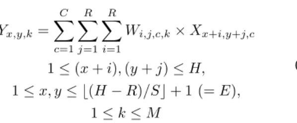
Yx,y,k= C X c=1 R X j=1 R X i=1 Wi,j,c,k× Xx+i,y+j,c 1 ≤ (x + i), (y + j) ≤ H, 1 ≤ x, y ≤ b(H − R)/Sc + 1 (= E), 1 ≤ k ≤ M (1)
where H is the width/height of the IFMP (with padding), E is the OFMP width/height (for a stride S), R is the filter width/height, C is the number of IFMP/filter channels and M is the number of filters/OFMP channels for a given CONV/FC layer. The width and height of the feature-maps/filters are assumed to be same for simplicity and also because it is very common in most of the popular CNNs.
In general, CNNs use real-valued inputs and weights. How-ever, in order to reduce their storage and compute complexity recent works have strived towards using small bit-widths to represent the input/filter-weight values. [6] proposed a binary-weight-network (BWN), where the filter weights (wi’s) can
be trained to be +1/-1 (with a common scaling factor per 3-D filter: α). This leads to a significant reduction in the amount of storage required for the wi’s, making it possible
to store them entirely on-chip. BWN’s also simplify the MAC operation to an add/subtract operation, since α is common for a given 3-D filter and it can be incorporated after finishing the entire convolution computation for that filter. As shown in [6], this algorithm does not compromise much on the original classification accuracy of the CNN, obtained using full precision weights. BWN performs better than binary-connect [7], which does not incorporate the scaling factor of α per filter, and also binarized-neural-networks [8], where both weights and activations are constrained to ±1.
Memory Compute Output Huge amount of data transfer to/from memory Memory with Embedded Computation Conventional all-digital implementation Proposed Memory-embedded implementation Buffer Buffer Input Outputs Input
No explicit data read Much less
data transfer
Fig. 2. Comparison of conventional approach vs. proposed approach of
memory-embedded convolution computation, for processing of CNNs.
In the conventional all-digital implementation of CNNs [4], [5], [9], with the memory and the processing elements being physically separate, reading the wi’s and the partial sums
from the on-chip SRAMs lead to a lot of data movement per computation [10] and hence, make them energy-hungry. This is because, in modern CMOS processes, the energy required to access data from memory can be much higher than the energy needed for a compute operation with that data [11]. To address this problem, we present an SRAM-embedded convolution computation architecture [12], conceptually shown in Fig. 2.
Embedding computation inside memory has two significant benefits. Firstly, data transfer to/from the memory is greatly re-duced, since the filter-weights are not explicitly read and only the computed output is sent outside the memory. Secondly, we can take advantage of the massively parallel nature of CNNs to access multiple memory addresses simultaneously. This is because we are only interested in the result of the computation using the memory data and not the individual stored bits. Therefore, a much higher memory bandwidth can be achieved with this approach, overcoming some of the major limitations posed by the conventional “von-Neumann bottleneck”.
This paper is organized as follows. Section II explains the concept of memory-embedded convolution computation as voltage averaging in SRAMs. Section III presents the overall architecture. Section IV highlights the key contributions of this work, compared to prior in-memory computing approaches. Section V discusses the details of the different circuitry involved in the embedded convolution computation. Section VI presents the measurement results. Finally, concluding remarks are discussed in section VII.
II. CONCEPT OFSRAM-EMBEDDEDCOMPUTATION
The basic operation involved in evaluating convolutions (Y ) for CNNs is the dot-product of the 3-D IFMP (X) and the filter-weights (W ), as shown in equation (1). It can be re-written by flattening the 3-D tensor into a 1-D vector to obtain equation (2), where the 2-D subscripts (x, y) have been omitted for simplicity. Yk = R×R×C X i=1 Wk,i× Xi (2)
Equation (2) can be further simplified for the case of binary filter-weights (wi’s) to get equation (3a), where αk is the
common coefficient for the kth filter. If α
k is expressed as
a ratio of two integers (Mk, N : number of elements added per
dot-product in 1 clock cycle), then we get equation (3b).
Yk = αk R×R×C X i=1 wk,i× Xi, wi∈ (+1, −1) (3a) =Mk N R×R×C X i=1 wk,i× Xi, Mk, N ∈ I+ (3b)
Now, if we separate out the scaling factor of Mk(which can
be incorporated after computing the entire dot-product), we get the expression for the effective convolution output (YOU T) as:
YOU T ,k= 1 N R×R×C X i=1 wk,i× XIN,i (4)
where XIN is the effective convolution input, i.e. scaled
version of the original input X, limited to 7-b (includes 1-b sign). For energy-efficient computation with multi-bit values inside the memory, equation (4) has to be implemented in the analog domain, as shown in equation (5).
VY AV G,k= 1 N R×R×C X i=1 wk,i× Va,i (5)
31.1: Conv-RAM: An Energy-Efficient SRAM with Embedded Convolution Computation for Low-Power CNN-Based Machine Learning Applications © 2018 IEEE
International Solid-State Circuits Conference 11 of 48
Binary-Weight CONV as Averaging in SRAMs
𝑌𝑂𝑈𝑇,𝑘 = 1 𝑁 𝑖 𝑤𝑘,𝑖× 𝑋𝐼𝑁,𝑖 𝑉𝑌_𝐴𝑉𝐺,𝑘 =𝑁1 𝑖 𝑤𝑘,𝑖× 𝑉𝑎,𝑖
DAC
ADC
1MAV
2 3 MAV: Multiply-and-AverageYOUT: Convolution Output || w: Binary Filter Weight || XIN: Convolution Input
Digital Domain
Analog Domain
Fig. 3. Concept of embedded convolution computation as averaging in
SRAMs for binary-weight convolutional neural networks.
The equivalence of equations (4) and (5), conceptually shown in Fig. 3, becomes apparent in 3 key steps. First, the digital inputs (XIN’s) are converted into analog voltages
(Va’s) using digital-to-analog converters (DAC). Then, the
analog voltages are multiplied by the corresponding 1-bit filter-weights (wi’s), which are stored in a memory array. This is
followed by averaging over N terms to get the analog-averaged convolution output voltage (VY AV G). These constitute the
second step: multiply-and-average (MAV). Finally, in the last step, the analog-averaged voltage is converted back into the digital domain (YOU T) using an analog-to-digital converter
(ADC), for further processing. It may be noted that if the 3-D filter size (R × R × C) is greater than N, the above-mentioned 3-step process is repeated multiple (Nr) times using R×R×C0
(≤ N ) elements in each cycle, where Nr= C/C0. The partial
outputs (from the ADC) can then be further added digitally (outside the memory) to get the final convolution output.
III. OVERALLARCHITECTURE
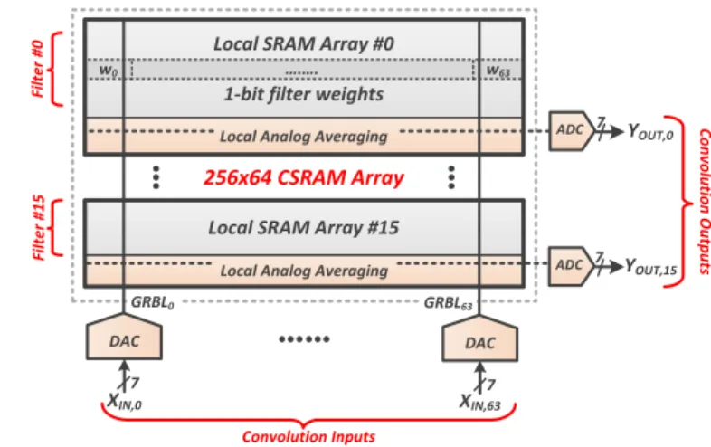
Fig. 4 shows the overall architecture of the 16 Kb Conv-SRAM (CConv-SRAM) array, consisting of 256 rows by 64 columns of SRAM bit-cells. It is divided into 16 local arrays, each with 16 rows. Each local array is meant to store the binary filter-weights (wi’s) for a different 3-D filter in a CONV/FC
layer. wi is stored in a 10T SRAM bit-cell as either a digital
‘0’ or a digital ‘1’, depending on whether its value is +1 or −1 respectively. The 10T bit-cell consists of a regular 6T bit-cell and 2 decoupled read-ports. Each local array has its analog averaging circuits (MAVa’s) and a dedicated ADC to
compute the partial convolution outputs (YOU T’s). Sharing
these circuits for 16 rows in a local array reduces the area overhead. The IFMP values (XIN’s) are fed into column-wise
DACs, which convert the digital XIN codes to analog input
voltages on the global bit-lines (GRBL’s). The GRBL’s are shared by all the local arrays, implementing the fact that in CNNs each input is shared/processed in parallel by multiple filters. With this architecture, the 16 Kb CSRAM array can process a maximum of 64 convolution inputs and compute 16 convolution outputs in parallel.
Fig. 5(a) shows the simulated test error-rates for the MNIST dataset with the LeNet-5 CNN, consisting of 2 CONV layers
Local SRAM Array #0 1-bit filter weights
Local Analog Averaging ….….
w0 w63
Local SRAM Array #15
Local Analog Averaging
YOUT,0 YOUT,15 DAC XIN,0 7 7 7 DAC XIN,63 7 GRBL0 GRBL63 Convolution Inputs Convolution Outputs Filter #0 Filter #15 ADC ADC
Fig. 4. Overall architecture of the Conv-SRAM (CSRAM) showing local
arrays, column-wise DACs and row-wise ADCs to implement convolution as weighted averaging.
(C1, C3) and 2 FC layers (F5, F6). The number of bits to represent the IFMP/OFMP values are varied from 8 to 4. Lower bit-width helps in reducing the area/power costs of the DAC and ADC circuits involved for the convolution computations. However, as seen from Fig. 5(a), the error rate starts to increase steeply for <7-b. Hence, 7-b is chosen as the target bit-width for the DAC/ADC circuits. With 7-b (including the sign bit) the voltage resolution needed on a 1 V scale is 1 LSB = 1/26≈ 15.6 mV. Next, the effect of the averaging factor (‘N ’) on the test error-rate is observed. A high value of ‘N ’ would decrease the area/power overhead of the ADC by amortizing it over more MAV operations per clock-cycle. However, higher ‘N ’ can also degrade the computation accuracy due to increased quantization by averaging. This is more crticial for CNN layers with smaller filter sizes. As shown in Fig. 5(b) for layer F6, with a 3-D filter size of 120, the error-rate steeply increases as ‘N ’ is varied from 15 to 120. For the other 3 layers of LeNet-5, the 2-D filter size is 5 × 5. Hence, a minimum N = 25 is required to fit at-least one full filter channel per CSRAM row. We chose N = 64 to fit 2 channels for 5 × 5 filters, without sacrificing much on the error rate. 0 2 4 6 8 10 12 14 16 0 2 4 6 8 10 4 5 6 7 8 DA C /A D C Cos t (normaliz ed) Te st Err o r Ra te (%) No. of bits for IFMP/OFMP 0 2 4 6 8 10 12 0 1 2 3 4 5 6 10 30 50 70 90 110 130 150 ADC Cost (normalized) Test Error Rate (%) Averaging factor (N) F6 F5 C3 (a) (b)
Fig. 5. Simulated results for the MNIST dataset with the LeNet-5 CNN by varying: (a) bit-width to represent IFMP/OFMP values, (b) averaging factor (N).
determines the unit capacitance (CLBL), which is used for all
the analog operations required for the in-memory convolution computation. For every column in a local array, there is a corresponding MAVa circuit. Hence, a higher value of Nrows
would decrease the area-overhead of MAVa, by amortizing
it over multiple rows. It also reduces variation of the CLBL
value, which helps in improving accuracy of the computations. However, a high value of Nrows means a high CLBL, which
translates to increased energy costs. It would also lead to less throughput for a given SRAM size, since fewer outputs would be computed per cycle. Therefore, Nrows= 16 is chosen as a
trade-off. It may be noted that with Nrows = 16, the thermal
noise (kTC) is < 1 mV, which is well below 1 LSB = 15.6 mV.
IV. KEY CONTRIBUTIONS OF THIS WORK
While there are a few different approaches [13]–[17] for in/near-memory computing, the proposed architecture has some key contributions, which provide significant benefits over prior work. The first key feature of our approach is the robust-ness to SRAM bit-cell Vtvariations. SRAM bit-cells use
near-minimum transistor sizes available in a given CMOS process and hence, suffer from transistor mismatch and variation. For example, if we consider the discharge current (Icell) through
an SRAM bit-cell (shown in Fig. 6) we can observe that it has a significant spread from its mean value (σ ≈ 30%µ). Now, when Icell is used to modulate the analog voltage (Va)
on the bit-line [13]–[15], [17], there is a wide variation in the Va value and it cannot be controlled very well. This
compromises the computation accuracy and extra algorithmic techniques might be required to compensate for that. [13] uses the ‘AdaBoost’ technique, in which the results of many weak classifiers are combined to get a more accurate final result. However, this would lead to an increase in the number of computations and the energy required. [15] proposed an on-chip training to compensate for chip-to-chip variations. However, this would incur energy and timing penalty required to re-train the network corresponding to every single chip. In our approach (Fig. 6), the analog voltage (Va) is directly sent
to the bit-lines using global DACs at the periphery. Since the global DACs can be upsized, with their area being amortized over mutliple rows (256 in this case), the variation due to it is significantly less compared to that of the bit-cell. Furthermore, the SRAM bit-cell is only used to multiply Vaby the 1-b filter
weight (wi) stored in it, using full signal swing locally. That
means, the purpose of the SRAM bit-cell is to discharge one of its local bit-lines to 0, it is not used to control Va. Hence,
given enough time for the worst-case bit-cell discharge, the computation accuracy does not suffer from local bit-cell Vt
variations.
The second key feature of our approach is the improvement of the dynamic voltage range for the analog computations without disturbing any bit-cell. In the conventional approach (with 6T SRAM bit-cells) [13], [14], [17], where multiple word-lines (WL) are activated for the same bit-line, there might be a situation where one of the accessed bit-cells in that column is in pseudo-write mode (Fig. 7). This is because multiple activated cells in that column can discharge a bit-line to a very low voltage, which could overwrite the data
DAC IN GBL a 10T x16 LBLT RWL LBLF a DAC IN Global Col Local Col 6T x16 x128 GBLT GBLF dd WL dd a Global Col MAV cell RWL cell dd
Conventional a cell Proposed a cell
VDD= 1.2V VWL= 0.6V SS 25˚C (a.u.) µ ≈ 3.1 (a.u.) σ ≈ 1.1 (a.u.) Icell (a.u.)
Fig. 6. Comparison of the conventional and proposed approaches of using
SRAM bit-cells for embedded analog computations.
stored (Qk = ‘1’) in the disturbed cell. Hence, the
bit-line voltage range has to be limited to prevent any write-disturb. In our approach, 10T bitcells are used which de-couple the read and the write ports, to prevent any write-disturb. Furthermore, each bit-cell is read independently in parallel without sharing any bit-lines. And hence, the discharge on one bit-line cannot affect another accessed bit-cell. Thus, we can utilize a wide voltage range (close to full-rail) for the analog computations, without disturbing any bit-cell. It may be noted that, although a 10T bit-cell has more transistors than a 6T, it can be designed using smaller sized devices, compared to a 6T bit-cell. This is because, unlike a 6T, a 10T bit-cell does not have conflicting sizing requirements to achieve high margins for both read and write operations. In addition, due to the limitations of 6T bit-cells for in-memory analog computations, network augmentation, i.e. larger sized neural networks, might be required to compensate for lower computation accuracy. Larger neural networks translate to increased storage requirement for filter-weights on-chip and hence, increased SRAM size. Therefore, overall, our 10T bit-cell based in-memory architecture is not necessarily higher area than a 6T based design.
The third key feature of our work, which distinguishes it from other “in-memory” computing approaches [14], [16], is the use of the inherent bit-line capacitances in the SRAM array to implement the computations. This precludes the need for extra area-intensive capacitors, which would be otherwise required at the SRAM periphery [14] to implement some of the analog computations.
Finally, this work supports multi-bit resolution for the inputs and outputs of the dot-products, compared to [13] (output: 1-b) and [16], [17] (both input/output: 1-b). This helps in achieving higher classification accuracy for a neural-network of a given size.
All the key features, described above, make our proposed architecture scalable i.e. multiple CSRAM arrays can operate in parallel to run larger neural networks.
GBLT GBLF WL0 WL1 WLk 0 1 0 1 1 0 Conventional Proposed Write Disturb WL 0 1 0 1 1 0 LBLT0 LBLF0 LBLT1 LBLF1 LBLTk LBLFk No Write Disturb GBLT GBLF Vdd Vdd 0 0 Qk Qk Data Flip 1 1 1 1
a,0 a,1 a,k
a,T a,F Va,T Va,F VWL 0 WLx
Fig. 7. Comparison of the conventional and proposed approaches on write-disturb issue of SRAM bit-cells during compute mode.
V. CIRCUITS FOR THE3-PHASECONV-SRAM OPERATION
A. Phase-1: DAC
During the first phase of the Conv-SRAM (CSRAM) op-eration the digital convolution input (XIN) is converted into
an analog voltage (Va) using a column-wise digital-to-analog
converter (GBL DAC). The analog voltage is used to pre-charge the global read line (GRBL) and the local bit-lines (not shown in Fig. 4) in the SRAM array. Each GRBL is shared by all the 16 local arrays and hence, they get the same value of the analog pre-charge voltage. This implements the fact that in a given CNN layer (CONV/FC) each input is processed simultaneously by multiple filters. Furthermore, all the 64 column-wise GBL DACs operate in parallel and can send a maximum of 64 analog inputs to the CSRAM array in one clock cycle.
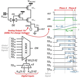
Fig. 8 shows the schematic of the proposed GBL DAC circuit. It consists of a cascode PMOS stack biased in the sat-uration region to act as a constant current source. The GRBL is charged with this fixed current for a time tON, which is
determined by the ON pulse-width. tON is modulated based
on the digital input code (XIN[5 : 0]), using a
digital-to-time converter. To achieve a very good linearity of Va vs
XIN or tON vs XIN, there should be a single continuous
ON pulse for every input code, to avoid non-linearities due to multiple charging phases. This is not possible to generate by simply using 6 timing signals with binary-weighted pulse-widths. However, it may be generated using 26 or 64 timing
signals and a 64:1 mux. But that would consume a lot of area, which is not ideal for a circuit that needs to be replicated for each column of the SRAM array. To address this issue, we present a 2-phase architecture in which the 3 MSBs of XIN
are used to select the ON pulse-width for the first half of charging and the 3 LSBs for the second half. A control signal (T D56) is used to choose between the 2 phases. In this way
an 8-to-1 mux, with 8 timing signals, can be shared during both the phases, to reduce the area overhead and the number
ON ON Vbiasp VDD,DAC GRBL RST MP1 MP2 MN 8:1 MUX ON 2:1 MUX SEL[2:0] 3 XIN[5:3] x3 XIN[2:0] 0 1 0 7 TD63 TD54 TD45 TD36 TD27 TD18 TD9 TD0 TD56 Digital Inputs Analog Output: Va (GRBL Pre-charge Voltage) 9t0 18t0 27t0 36t0 45t0 54t0 63t0 56t0 7t0 TD63 TD54 TD45 TD36 TD27 TD18 TD9 TD0 TD56 RST ON GRBL XIN= 63 XIN= 24 1V 0 Global Timing Signals Phase A Phase B Select Signal
Fig. 8. Schematic of the column-wise GBL DAC circuit, showing the digital-to-time converter (bottom-left) and time-to-analog converter (top-left). Also shown are the timing signals and operation waveforms for 2 input codes (right).
of timing signals to route. A tree-based architecture, using 2:1 unit mux’s, is used for the 8:1 mux to equalize the mux-delay for different control bits.
To design the pulse-widths of the 8 timing signals, we need to express XIN in terms of its 2 components:
XIN,dec= 8 × kA+ kB,
kA= Decimal(XIN[5 : 3]),
kB = Decimal(XIN[2 : 0])
(6)
where kA and kB are the decimal values for the 3 MSBs
and the 3 LSBs of XIN respectively. Since kA and kB can
have any integer values from 0 to 7, the pulse-widths of the timing signals (T D’s) are chosen as:
tT D9k= 8 × kt0+ kt0= 9 × kt0
k ∈ (0, 1, .., 7) (7)
where t0 is the minimum time resolution. A delay-line
architecture, with a controllable unit delay of t0, is used to
generate 64 time-delayed signals from the input clock. Then the appropriate signals are combined using NOR gates to generate the T D’s. This is done at the global level and the generated T D’s are buffered and routed to all the GBL DACs. A higher value of t0reduces the non-linearities from the timing
generation circuitry, at the cost of increased clock cycle time. To understand how the 2-phase charging technique works, let us consider two XIN values of 24 and 63, as shown in
Fig. 8. For XIN = 24 = 8 × 3 + 0, kA is 3 and kB is 0.
Hence, T D9×3 or T D27 is used in phase A and T D0is used
in phase B, to select the pulse-width of the ON timing signal. Similarly, for the code XIN= 63 = 8×7+7, both kAand kB
are 7 and hence, T D63 is used in both the charging phases.
In addition to the linearity aspect of the DAC transfer function, this architecture also performs better in terms of
de-vice mismatch, compared to binary-weighted PMOS charging DACs [13]. This is because, here, the same PMOS stack is used to charge the global bit-line for all input codes, rather than having to use smaller PMOS devices for small input values. Furthermore, the pulse-widths of the globally generated timing signals have less variations typically, compared to those arising from local Vt-mismatch in the PMOS devices [13].
It may be noted that, a one-time calibration is required to set the maximum value of the analog pre-charge voltage for the maximum input code (XIN,max). The maximum
pre-charge voltage should be kept lower than the supply voltage of the GBL DAC, to ensure that the PMOS cascode stack is operating in the saturation region as a constant current source. For a given t0, the calibration can be achieved by tuning the
externally provided bias voltage (Vbiasp) of the PMOS stack.
During calibration, all DACs are fed the same input value of XIN,max. In a given clock cycle, first, the GBL DAC
pre-charges the GRBL to an analog voltage (Va). Then, Va is
compared to an externally provided reference voltage Vref
(typically kept at 1 V in this work). The comparison is done by the column-wise sense-amplifiers (SA), which are already present for normal read-out of the SRAM. All the 64 SAs operate in parallel and use the same Vref to provide 64
comparison outputs simultaneously. Vbiasp is monotonically
increased from 0 V until majority of the SAs (> 50%) flip their outputs (‘1’ to ‘0’), at which point the calibration is achieved. In this work, a 5 mV step-size is used to tune Vbiasp.
B. Phase-2: Multiply-and-Average
The second phase of the Conv-SRAM operation involves the mutliplication of the analog input voltages (Va’s) with the
1-b filter weights (wi’s) and averaging over N values. This
multiply-and-average (MAV) operation is done in parallel for all the 16 local arrays, each storing the wi’s for a different
3-D filter when running a CONV/FC layer.
VY AV G,k= 1 N N X i=1 wk,i× Va,i, 0 ≤ k ≤ 15, N ≤ 64 VY AV G= V pAV G− V nAV G (8)
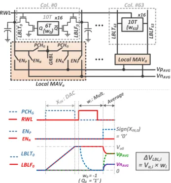
Fig. 9 shows the details for the MAV operation for one local array. It starts by turning on the read word-line (RW L) for the selected row in the local array. This leads to discharging of one of the local bit-lines (LBLT, LBLF ) in each column, depending on the wi stored in the corresponding 10T bit-cell.
A positive wi (+1) is stored as a digital ‘0’ and a negative
wi (−1) as a digital ‘1’. It may be noted that, the local
bit-lines have been pre-charged to the same analog voltage (Va,i)
as its corresponding global bit-line (GRBL) during phase-1. Therefore, at the end of weight evaluation, the difference between the local bit-line voltages represents the product of the analog voltage (Va,i) and the 1-b weight (wi). For example, the
bit-cell in the ‘0th’ column stores a −1 and hence, ∆VLBL,0=
VLBLT ,0− VLBLF,0 = −Va,0.
The weight multiplication/evaluation step is completed by turning off the RW L. After that, the appropriate local bit-lines are shorted together horizontally to evaluate the average. The
PCHG RWL ENP ENN XIN : D AC wi : M ult. LBLT0 LBLF0 w0 = -1 ( Q0= ‘1’ ) VpAVG VnAVG Va0 0 Sign(XIN,0) = ‘0’ Avera ge Local MAVa PCHG ENN
ENP ENN ENP
10T (w63) Local MAVa LB LT63 LBLF 63 LB LT0 LBLF 0 GRBL RWL x16 x16 Col. #0 Col. #63 6T (w0) Q Q 10T VpAVG VnAVG PCHG ΔVLBL,i = Va,i× wi
Fig. 9. Architecture of a 16×64 local array of the Conv-SRAM, showing the 10T bit-cells storing the filter weights and local analog multiply-and-average (MAVa) circuits. Also shown are typical operation waveforms (bottom) for
one column.
positive and negative parts of the average as obtained on two separate voltage rails, V pAV Gand V nAV G, respectively. This
is implemented by the local MAVa circuits, which pass the
voltages of the LBLT ’s and LBLF ’s to either the V pAV G
or the V nAV G voltage rails, depending on the sign of the
input XIN. If the input for the particular column is positive
(XIN > 0) ENP is turned on, otherwise ENN is on.
ENP and ENN are digital control signals which are globally
routed and shared column-wise by all the 16 local arrays. The switches controlled by ENP and ENN are implemented
using NMOS pass transistors, since the final V pAV G, V nAV G
voltages would be closer to 0 V than Vref. On the other hand,
the switches controlled by P CHG use CMOS transmission
gates, since they need to pass a wide range of voltages from 0 V to Vref (∼ 1 V), during phase-1 (DAC pre-charge).
The fully-differential nature of the averaging architecture helps in mitigating many common-mode noise issues, e.g. clock coupling noise from the control switches, capacitance variation of the local bit-lines and the voltage rails due to different process corners, etc. This helps in improving the accuracy of the dot-product computations with our approach. It may be also noted that during this phase, when the SRAM bit-cell is actually used for weight-evaluation, the time required does not have a huge variation. Fig. 10 shows the simulated local bit-line discharge time (tdis,LBL ) in the
slowest process corner (SS). As seen from the figure, even the 6σ value of tdis,LBLis merely 500 ps, which is much smaller
than the total clock period (≈ 100 ns). This shows that bit-cell Vt variations do not dominate the overall computation time.
The longer clock period is justified due to the highly parallel processing in the compute mode.
BL WL
Fig. 10. Variation of the local bit-line discharge time for weight evalua-tion/multiplication in phase-2.
C. Phase-3: ADC
The third and last phase of the Conv-SRAM operation is the analog-to-digital conversion of the dot-product outputs, with multi-bit resolution. The difference of the analog average voltages (V pAV G and V nAV G) is fed to an ADC to get
the digital value of the computation (YOU T). This is done
in parallel for all the 16 local arrays, producing outputs corresponding to 16 different filters simultaneously.
Choosing the ADC architecture is crucial since it would be replicated multiple times in the CSRAM array. Hence, area and power consumption are key metrics to consider. In addition, the typical distribution of the ADC outputs (YOU T’s) should
also be considered to find the more appropriate architecture. As seen from simulation results in Fig. 11, for a typical CONV layer with a full scale input range of ±31, YOU T has an
absolute mean value of ±1.3 and is typically limited to ±7. Hence, a serial integrating ADC architecture is more suitable in this scenario, compared to other area-intensive (e.g. SAR) and more power-hungry ones (e.g. flash). In spite of its serial nature, in most cases we can expect the ADC to finish its operation within a few cycles, due to the particular YOU T
distribution.
Fig. 11. Simulated distribution of the partial convolution output from the
ADC (YOU T), for a typical CONV layer (C3) in the LeNet-5 CNN.
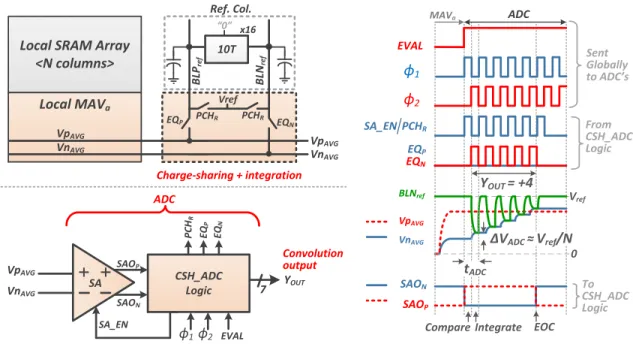
Fig. 12 shows the architecture of the proposed integrating ADC (CSH ADC). It consists of 3 main parts: a charge-sharing based integrator, a sense-amplifier (SA) and a logic block. Capacitive charge-sharing with replica bit-lines is used to implement the integration. The use of replica bit-lines helps
to track the local bit-line capacitance better in the presence of process and temperature variations. The SA has a standard StrongARM latch-type architecture. PMOS devices are chosen for the input differential pair of the SA, since the common mode voltages of V pAV Gand V nAV Gsignals are expected to
be closer to the GND rail. The logic block provides the timing signals for the charge-sharing (P CHR, EQP, EQN) and the
SA comparison (SA EN ), using the globally provided timing signals (φ1, φ2). It also has a counter to count the number of
cycles it takes to finish the ADC operation and that provides the digital output of the dot-product computation.
Fig. 12 also shows the waveforms for a typical CSH ADC operation. It starts by sending a SA EN pulse from the ADC logic block to the SA. The SA compares V pAV Gand V nAV G,
and sends its outputs (SAOP, SAON) to the ADC logic
block. The first comparison determines the sign of the output, e.g. for the case shown in Fig. 12, YOU T is positive since
V pAV G is higher than V nAV G. After the first comparison,
the lower of the 2 voltage rails (V nAV G) is integrated by
charge-sharing it with a reference local bit-line (BLNref),
using the equalize signal (EQN in this case). The reference
bit-line, which replicates the local bit-line capacitance, was pre-charged during the SA comparison using the P CHR
signal to Vref (= 1 V in this work). Therefore, the
step-size of the integration is ≈ Vref
N , where N is the number of
SRAM local columns that were averaged. The pre-charge and equalize/integrate operations, along with the SA comparison, continue until the lower voltage rail (V nAV G) exceeds the
higher one (V pAV G). When this happens, the SA outputs
flip indicating the end-of-conversion (EOC). After this, no more timing pulses are generated. A counter in the ADC logic block counts the number of equalize pulses (EQN) it
takes to reach EOC and that generates the digital value of the convolution/dot-product output (YOU T), which is +4 for
the example shown in Fig. 12.
FLIP FLIP FLIP AVG AVG SA_EN OUT OS CLK FLIP
Cycle 0: “Odd”Cycle 1: “Even”
Fig. 13. Circuit for the 2-cycle offset-cancellation technique for the SA in CSH ADC.
It may be noted that YOU T is directly affected by the SA
offset voltage (VOS), which can degrade the overall
compu-tation accuracy due to incorrect ADC outputs. To address this issue, we propose a simple 2-cycle offset-cancellation technique, using a flipping mux at the input of the SA (Fig. 13). During the first/even cycle of this 2-cycle period, F LIP = ‘0’. Hence, V pAV G and V nAV Gare passed to the positive
10T BL Pref BL Nre f x16 Ref. Col. “0” PCHR PCHR EQP EQN Vref Charge-sharing + integration VpAVG VnAVG ADC Local SRAM Array
<N columns> Local MAVa VpAVG VnAVG CSH_ADC Logic
+
+
VpAVG VnAVG SA_EN Convolution output YOUT 7 SA PC HR EQ P EQ N EVAL SAOP SAON 0 ADC MAVa EVAL SA_EN PCHR EQN VpAVG VnAVG EQP SAON SAOP tADC BLNref Vref ΔVADC ≈ Vref/NCompare Integrate EOC
YOUT = +4 From CSH_ADC Logic To CSH_ADC Logic Sent Globally to ADC’s
ϕ
2ϕ
1 ϕ2 ϕ1Fig. 12. Architecture (left) for the charge-sharing based ADC (CSH ADC) for 1 local array of the Conv-SRAM and typical waveforms (right) for the digital output (YOU T) computation for the convolution (dot-product) operation.
YOU T ,0 = ADC(V yAV G,0− VOS). The output in this cycle
is exactly same as in the conventional case (without the flipping mux). However, during the next odd cycle, the inputs to the SA are flipped by setting F LIP = ‘1’. Hence, a differential voltage of (V nAV G − V pAV G) = −V yAV G is
applied to the input of the SA. To get the correct polarity at the output of the ADC, another negation is applied by the ADC logic block. This results in YOU T ,1 = −ADC(−V yAV G,1−
VOS) = ADC(V yAV G,1+ VOS), as compared to YOU T ,1 =
ADC(V yAV G,1− VOS) for the conventional case. Finally, we
add the YOU T’s for the 2 consecutive cycles to accumulate the
partial results for the convolution. With our proposed 2-cycle approach the effect of VOS is inherently canceled since:
YOU T = YOU T ,0+ YOU T ,1
= ADC(V yAV G,0+ V yAV G,1)
(9) On the other hand, for the conventional case the effect of VOS adds up since:
YOU T = ADC(V yAV G,0+ V yAV G,1− 2 × VOS) (10)
and this makes the accumulation result further inaccurate. It may be noted that, the benefits of this offset-cancellation technique comes without any extra timing and power penalty, as long as an even number of cycles are required to finish a full convolution computation. This can be easily expected for most CNNs.
VI. MEASUREDRESULTS
The 16 Kb CSRAM array was implemented in a 65-nm LP CMOS process. The die photo in Fig. 14 shows the relative area occupied by the different key blocks. The bit-cell array (ARY) along with its peripheral circuitry occupies 73.1% of the total CSRAM area, 8.2% is occupied by the GBL DACs,
8.6% by the local MAVa circuits, 7.3% by the CSH ADCs
and the rest by global timing circuits. The test-chip summary is shown in Table I.
Fig. 14. Die micro-photograph in a 65-nm CMOS process.
A. Circuit Characterizations
Fig. 15 shows the measured transfer function of the 6-b GBL DAC. With Vref = 1 V and t0≈ 250 ps, a 5-b voltage
resolution is effectively achieved in measurements. Hence, we set the LSB of XIN to ‘0’. To estimate the DAC analog
output voltage (Va), VGRBLfor the 64 columns of the CSRAM
are compared to an external voltage (Vref) by column-wise
SAs, as explained before for DAC calibration (Section V-A). For each XIN, the Vref at which more than 50% of the
SA outputs flip is chosen as an average estimate of Va. As
mentioned before, an initial one-time calibration is needed to set Va,max= 1 V for XIN = 31 (max. input code). The supply
TABLE I TEST-CHIPSUMMARY
Technology 65-nm CSRAM size 16 Kb CSRAM area 0.063 mm2 Array organization 256×64 (10T bit-cells) # column DACs 64 # row ADCs 16 Max. # MAVs 64×16 Supply voltages 1.2 V (DAC), 0.8 V (array), 1 V (rest) Main clock freq.
(compute mode) 5 MHz
ADC clock freq. 250 MHz
-0.6 -0.4 -0.2 0 0.2 0.4 0.6 0.8 400 500 600 700 800 900 1000 1100 31 29 27 25 23 21 19 17 DNL (L SB) V a (mV) XIN (scaled to 5-b) Va Videal DNL
Fig. 15. Measured transfer function of GBL DAC at Vdd,DAC = 1.2 V,
with Vref = 1 V and t0≈ 250 ps.
stack in them operating in the saturation region (as a constant current source). It can be seen from Fig. 15 that there is a good linearity in the DAC transfer function with DN L < 1 LSB. Since the SAs have NMOS input-pair, low values of Va
cannot be properly estimated. Hence, the characterization is done till XIN = 16 (or Va≈ 500 mV).
0.6 0.8 1 1.2 1.4 1.6 1.8 ‐11 ‐9 ‐7 ‐5 ‐3 ‐1 1 3 5 7 9 11 0 1 2 3 4 5 6 7 E ADC (pJ) Y OUT XIN (scaled to 5‐b) w: '0' (+1) w: '1' (‐1)
Fig. 16. Measured transfer function and energy consumption of CSH ADC
at Vdd,ADC = 1 V, Vdd,ARY = 0.8 V and fADC = 250 MHz.
Fig. 16 shows the transfer function of the CSH ADC, operating at 1 V and a clock frequency of 250 MHz (gen-erated on-chip with a free-running VCO). The array voltage (Vdd,ARY) is kept at 0.8 V to reduce the clock-coupling noise
from the W L’s, when reading the weights. To characterize
the CSH ADCs, all XIN’s are fed the same input code, all
wi’s are written the same value and then the ADC outputs
(YOU T ’s) are observed. The measurement results show a good
linearity in the overall transfer function and low variation in the YOU T values, which is due to the fact that the variation
in BL capacitance (used in CSH ADC) is much lower than transistor Vt-variation. It can be also seen from Fig. 16 that
the energy/ADC scales linearly with the input/output value, which is expected for the integrating ADC topology.
|Y OUT | (scaled to 5-b) -1 0 1 2 3 No. of occurences 0 5 10 15 20 25 30 X IN = 0 w/o OC w/ OC |Y OUT | (scaled to 5-b) 3 4 5 6 7 8 No. of occurences 0 5 10 15 20 25 X IN = 4 w/o OC w/ OC
Fig. 17. Measured distribution of convolution output values (YOU T) from
CSH ADC with and without the offset-cancellation (OC) technique, for two values of the input code (XIN).
The effect of the offset-cancellation (OC) technique for the SA (in the CSH ADC) is also characterized, as shown in Fig. 17 for two different input codes. It can be clearly seen that the OC helps in reducing the variation of the YOU T
values, leading to a better computation accuracy for the dot-products/convolutions.
B. Test Case: MNIST Dataset
CNN Layers: C1 S2 C3 S4 F5 F6 5×5 CONV 5×5 CONV MAXPOOL2×2 5×5 FC 1×1 FC 2×2 MAXPOOL 28×28×6 28×28×1 14×14×6 10×10×16 5×5 ×16 1×1×120 1×1 ×10 Input 0 9 1 2 3 4 5 6 7 8
Fig. 18. Architecture of the LeNet-5 CNN, showing the sizes of the feature maps (top) and the filters (bottom).
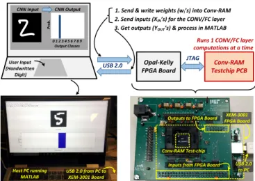
To demonstrate the functionality for a real CNN architec-ture, the MNIST hand-written digit recognition dataset is used with the LeNet-5 CNN [18]. As shown in Fig. 18, LeNet-5 consists of 2 CONV layers (C1, C3) and 2 FC layers (F5, F6). In addition, there are 2 sub-sampling or max-pooling layers (S2 and S4, following layers C1 and C3 respectively) and a non-linear ReLU layer (R5 after layer F5). Only the CONV/FC layers, which involve majority of the computations, are implemented on-chip by the CSRAM array. The non-linear layers are implemented in software. Fig. 19 shows the test setup used to automatically run the 4 CONV/FC layers, one
TABLE II
PARAMETER MAPPING FOR THECONV/FCLAYERS OFLENET-5 CNNTO
THECSRAMARRAY
Parameters (↓) C1 C3 F5 F6
3-D Filter size 5×5×1 5×5×6 5×5×16 1×1×120
# 3-D Filters 6 16 120 10
# Local ARYs used 6 16 15† 10
# IFMP channels/row 1 2 2 30*
Rows, Col.s/local ARY 1, 25 3, 50 8, 50 4*, 30*
# col.s for AVG (N ) 32 50 50 32
# operations/cycle 25×6×2 50×16×2 50×15×2 30*×10×2
†Repeated 8 times to cover all the 120 filters
*15 columns and 8 rows mapping used at V
DD = 0.8 V
after the other, on the test-chip. Data is transferred back and forth between MATLAB (running on a host PC) and the test-chip, via an FPGA board. Table. II shows the detailed mapping of the 4 CONV/FC layers to the CSRAM array to compute the convolutions. Let us first consider layer C3. It has a filter size of 5 × 5, with 6 input channels and 16 output channels (number of 3-D filters). Each of the 16 3-D filters are mapped to one of the 16 local arrays in the CSRAM. Since each row in the local array has 64 bit-cells, a maximum of 2 (= b5×564 c) input channels can fit per row. Therefore, 3 (= 62) rows are required in each local array to fit the entire 3-D filter. In every clock cycle, 50 (= 5 × 5 × 2) XIN’s are sent through
a buffer (shift-registers) to the CSRAM array to compute 16 partial convolution outputs. Thus, the CSRAM array processes 50 × 16 × 2 operations (1 MAV = 2 OPs: 1 multiply + 1 add/average) per clock cycle. For layer F5, the entire filter cannot fit at once in the CSRAM array (due to its limited 16 Kb size in the test-chip). Hence, the entire process, explained above, is repeated multiple times to finish all the computations. However, having multiple CSRAM arrays operating in parallel can easily alleviate this problem, by fitting all the filter weights together on-chip. 0 1 2 3 4 5 6 7 8 9 Output Classes Prob. CNN Input CNN Output Opal-Kelly FPGA Board Conv-RAM Testchip PCB User Input (Handwritten Digit)
1. Send & write weights (wi’s) into Conv-RAM 2. Send inputs (XIN’s) for the CONV/FC layer 3. Get outputs (YOUT’s) & process in MATLAB
Runs 1 CONV/FC layer computations at a time USB 2.0 JTAG USB 2.0 to PC XEM-3001 FPGA Board Outputs to FPGA Board
Inputs from FPGA Board USB 2.0 from PC to
XEM-3001 Board Host PC running
MATLAB
Conv-RAM Test-chip
Fig. 19. Test setup for automatically running the 4 CONV/FC layers of
LeNet-5 CNN on Conv-SRAM, for a given input image (28 × 28).
Fig. 20 shows the measured error rate for the 10,000 test images in the MNIST dataset, with the 4 CONV/FC layers being successively implemented on-chip. 3 different chips are
measured, each experiment is repeated multiple times, and the average value of the error rate is reported. We tested 2 different versions of LeNet-5: with and without Batch-Normalization (BN) layers preceeding the CONV/FC layers. Without BN layers (‘v1’) we achieve a classification error rate of 2.5% after all the 4 layers. The error rate is improved to 1.7% by using the BN layers (‘v2’). This is mostly because BN normalizes the convolution inputs for every layer, with a mean around 0 and also limits the maximum value of the inputs. Hence, after input quantization to 6-b, its features are better preserved compared to an un-normalized input distribution. The measured error rate, which is close to the expected value from an ideal digital implementation, shows the robustness of the CSRAM architecture to compute convolutions. The error rate for the MNIST dataset is improved by 8.3% compared to prior work on in/near-memory compute [13], [16], where a 10% error rate was achieved. Next, we tested functionality at a lower voltage setting of Vdd,DAC = 1 V and the rest of the
circuits operating at Vdd (rest) = 0.8 V, with a clock period
of 400 ns. The maximum DAC pre-charge voltage (Va,max),
corresponding to the maximum input code, is calibrated to 0.8 V. Hence, the magnitude of 1 LSB is ∼ 26 mV (instead of 32 mV for the previous case with Va,max = 1 V). Fig. 21
shows the measured error rate for this set of voltages. Due to reduced analog voltage precision, the error rates are slightly higher, with ‘v1’ achieving 3.4% and ‘v2’ achieving 1.9% for the MNIST test dataset.
0.00 1.00 2.00 3.00 4.00 5.00 C1 C3 F5 F6 Err o r Rate (%) Layer successively implemented by CSRAM v1: w/o BN v2: w/ BN Ideal (v1) ~1.56% Ideal (v2) ~1.19%
Fig. 20. Measured error rate for the 10K images in the MNIST test dataset
using LeNet-5 CNN, with and without BN, at Vdd= Va,max= 1V.
0.00 1.00 2.00 3.00 4.00 5.00 C1 C3 F5 F6 Err o r Rate (%) Layer successively implemented by CSRAM v1: w/o BN v2: w/ BN Ideal (v1) ~1.56% Ideal (v2) ~1.19%
Fig. 21. Measured error rate for the 10K images in the MNIST test dataset
using LeNet-5 CNN, with and without BN, at Vdd= Va,max= 0.8V.
The distributions of the partial convolution outputs from the ADC (YOU T’s) are shown in Fig. 22, for all the 4 CONV/FC
layers. For each of these layers, YOU T has a mean around ≈
1 LSB, which justifies the use of the serial ADC topology to compute it. Fig. 23 shows the distributions of the convolution inputs (XIN’s) for the 4 layers. XIN’s have been properly
CONV Layer C1 -10 -5 0 5 10 Y OUT 0 2 4 6 No. of occurences 106 CONV Layer C3 -10 -5 0 5 10 Y OUT 0 0.5 1 1.5 2 No. of occurences 106 FC Layer F5 -10 -5 0 5 10 YOUT 0 2 4 6 No. of occurences 105 FC Layer F6 -5 0 5 YOUT 0 0.5 1 1.5 2 No. of occurences 104 Abs. Mean ~0.3 LSB Abs. Mean ~1.3 LSB Abs. Mean ~0.8 LSB Abs. Mean ~1.0 LSB
Fig. 22. Measured distribution of the partial convolution outputs (YOU T’s)
for the 4 different CONV/FC layers of the LeNet-5 CNN.
scaled and quantized to 6-b (including sign bit) before being sent to the CSRAM array to compute the convolutions. As seen from the figure, all the layers have a high proportion of 0’s for the XIN’s. This helps in reducing the GBL DAC energy to
convert and send them to the columns of the CSRAM array.
CONV Layer C1 -10 0 10 20 30 XIN 0 1 2 3 4 No. of occurences 105 CONV Layer C3 -20 0 20 XIN 0 2 4 6 8 No. of occurences 105 FC Layer F5 -20 0 20 XIN 0 2 4 6 No. of occurences 104 FC Layer F6 0 10 20 30 XIN 0 2 4 6 8 10 No. of occurences 104 Abs. Mean ~ 4.7 # 0's = 45.2% # '0'-bits = 76% Abs. Mean ~ 6.7 # 0's = 57.8% # '0'-bits = 79% Abs. Mean ~ 3.1 # 0's: 80.3% # '0'-bits = 91% Abs. Mean ~ 8.0 # 0's: 14.7% # '0'-bits = 68%
Fig. 23. Measured distribution of the 6-b convolution inputs (XIN’s) for
the 4 different CONV/FC layers of the LeNet-5 CNN.
Fig. 24 shows the overall energy consumption of the CSRAM array for running the different layers of LeNet-5, with Vdd,DAC = 1.2 V, Vdd,ARY = 0.8 V, Vdd (rest) = 1 V
and fclk = 5 MHz. Of the 4 CONV/FC layers in LeNet-5,
the energy consumptions while running layers C1 and F6 are lower than that of layers C3 and F5. This is because layers C1 and F6 do not fully utilize the entire CSRAM array, due to their small filter sizes. However, that also translates to a lower energy-efficiency for these layers (Table III), since the energy is amortized over fewer MAV operations. A higher array utilization in layer C3 (all 16 local arrays) helps in achieving an energy-efficiency of 38.8 TOPS/W (‘v1’), by consuming 41.3 pJ of energy for 50×16×2 = 1600 operations.
Whereas, for ‘v2’ (with BN), layer F5 achieves the best energy-efficiency of 40.3 TOPS/W, utilizing 15 of the 16 local arrays. Fig. 24 also shows the energy breakdown for the 3 major components: GBL DAC, ARY+MAVaand CSH ADC.
The energy for the GBL DACs is limited by the bit-precision requirement for representing the IFMP values. Whereas, the energy for the ARY, MAVa and CSH ADC circuits can be
scaled down by scaling their supply voltages while sacrificing speed. Fig. 25 shows the measured energy consumption of the CSRAM array, with Vdd,DAC= 1 V, Vdd(rest) = 0.8 V and fclk
= 2.5 MHz. The reduced supply voltages help in decreasing the energy consumption, leading to better energy-efficiency numbers (Table IV).
0 10 20 30 40 50 60 v1 v2 v1 v2 v1 v2 v1 v2 C1 C3 F5 F6 Ener gy (pJ) LeNet‐5 CNN Layer
GBL_DAC ARY & MAVa CSH_ADC
v1: w/o BN, v2: w/ BN
Fig. 24. Measured energy consumption of the CSRAM array when running
the 4 different CONV/FC layers of the LeNet-5 CNN, with Vdd,DAC = 1.2
V, Vdd,ARY = 0.8 V, Vdd(rest) = 1 V and fclk,main= 5 MHz.
TABLE III
MEASURED ENERGY-EFFICIENCY* (TOPS/W)FOR THECONV/FC LAYERS OFLENET-5 CNN,ATVdd= 1V
Type (↓) C1 C3 F5 F6
v1: without BN 14.8 38.8 38.8 24.3
v2: with BN 14.7 33.5 40.3 23.2
*1 MAV = 1 multiply + 1 average = 2 OPs, with 6-b inputs and 1-b weights
0 5 10 15 20 25 30 35 v1 v2 v1 v2 v1 v2 v1 v2 C1 C3 F5 F6 Ener gy (pJ) LeNet‐5 CNN Layer
GBL_DAC ARY & MAVa CSH_ADC
v1: w/o BN, v2: w/ BN
Fig. 25. Measured energy consumption of the CSRAM array when running
the 4 different CONV/FC layers of the LeNet-5 CNN, with Vdd,DAC= 1 V,
Vdd(rest) = 0.8 V and fclk,main= 2.5 MHz.
Recent hardware implementations [5], [9], [16], [19]–[21] for NNs have focused on reduced bit-precisions to achieve higher energy-efficiency. Table V presents comparison with
TABLE V
COMPARISON WITH PRIOR WORK ON LOW BIT-WIDTH HARDWARE IMPLEMENTATIONS OFMLALGORITHMS
Metric This work ISSCC’17[9] JSSC’17[5] JSSC’17[13] JSSC’18[14] JSSC’18[16] CICC’18[19] ISSCC’18[20]
Tech. (nm) 65 28 40 130 65 65 28 65
Voltage (V) 1 0.715 0.8 - 1 0.55 0.66 0.65
Computation Mode
In-Memory,
mixed-signal Digital Digital
In-Memory, mixed-signal In-Memory, mixed-signal Near-Memory, digital Digital Digital ML Algo. CNN (4-layer) FC-DNN (4-layer) CNN (5-layer) SVM 1 k-NN2 FC-DNN (12-layer) CNN (5-layer) CNN
ML Dataset MNIST MNIST MNIST MNIST MNIST MNIST MNIST FER2013
# MAC(V)’s per classification 406.8K 334.3K 406.8K 3.65K 1 16.4K 768.1K 15M -Classification Accuracy 98.3% (1V) 98% (0.8V) 98.36% 98% 90% 92%2 90.1% 97.4% -# bits for IFMP/OFMP 6 8 6 5/1 8 2 1 16 # bits for Weights 1 8 4 1 8 1 1 1 SRAM Size (KB) 2 1024 144 2 16 102.1 328 256 Peak Throughput (GOPS)3 8 (1V) 4 (0.8V) 10.7 102 57.61 10.2 380.2 90 368.6 Peak Energy Efficiency (TOPS/W) 40.34(1V), 51.34(0.8V) (0.345)1.86 5 (0.663)1.75 5 11.51 1 (46.0)5 1.94 6.0 (24.12)130 5 50.6
1SVM: Support Vector Machine with 45 binary classifiers, each with 81 inputs, i.e. 81 × 45 MACs per 10-way classification 2k-NN: k-Nearest Neighbor, only 4-output classes (out of 10) were demonstrated with 100 test images
3We assume 2 operations (OPs) for 1 MAV (1 mult. + 1 avg.), similar to a MAC (1 mult. + 1 acc.)
4Does not include energy to access IFMP/OFMP memories
5Assuming a 65-nm implementation and Energy ∝ (Tech.)2
TABLE IV
MEASURED ENERGY-EFFICIENCY* (TOPS/W)FOR THECONV/FC LAYERS OFLENET-5 CNN,ATVdd= 0.8V
Type (↓) C1 C3 F5 F6
v1: without BN 19.7 49.6 48.9 17.0
v2: with BN 19.6 51.3 49.6 16.5
*1 MAV = 1 multiply + 1 average = 2 OPs, with 6-b inputs and 1-b weights
prior work, both conventional digital [5], [9], [19], [20] and in-memory approaches [14], [16]. It should be noted that, while [5], [9], [16], [19], [20] are full systems, the main focus of this work was to demonstrate in-memory computation capability for CNNs. Hence, ours does not include the energy for IFMP/OFMP memories. However, for the MNIST dataset with LeNet-5 CNN, we estimate [22] those to have only small contributions to the overall energy-efficiency per MAV opera-tion, due to the high parallelism supported by our in-memory approach. Furthermore, as seen from Fig.s 23 and 22, both the inputs (XIN’s) and the partial outputs (YOU T’s) have a
high proportion of ‘0’s. Hence, in future work, data-dependent memory architectures e.g. 8T SRAMs, [23], [24] can be used to store and access the inputs/outputs. [23], [24] take advantage of data properties to significantly reduce memory-access energy, which would be highly useful here. Compared to [5], [9], we achieve > 27× improvement in
energy-efficiency, due to the massively parallel in-memory analog computations. Our work achieves similar energy-efficiency numbers as [19] (considering a simplified technology scaling model), while using 6-b for IFMP/OFMP, compared to 1-b in [19]. Whereas, we achieve similar classification accuracy as [19] on MNIST, using ∼ 37× less MAC/MAV operations per classification. Our numbers are also comparable to the energy-efficiency of [20] (not quoted for MNIST), which uses 1-b for weights. Next, we compare our results to an in-memory mixed-signal computing approach [13], which implements a support vector machine (SVM) algorithm with 45 binary-classifiers, for a 10-way MNIST digit classification. We achieve similar energy-efficiency as [13], while improving the classification accuracy from 90% to > 98%. This is because, we mitigate the problem of degraded computation accuracy, caused by SRAM bit-cell variation. Although [13] can run at a higher speed, it only supports 1-b output resolution, compared to 6-b in our case. When compared to a near-memory approach [16], which uses only 1-b for IFMP/OFMP, we still achieve 8.5× improvement in energy-efficiency. This is because, our ap-proach exploits high parallelism of accessing multiple memory addresses simultaneously, without the need to sequentially and explicitly read out the data (filter weights) from the memory. We also achieve a higher classification accuracy compared to [16], because of using 6-b for inputs/outputs. Finally, our
work also achieves better classification accuracy than prior in-memory approach [14], although it supports 8-b weights. This is because we reduce the effect of bit-cell variation when evaluating the weights. In addition, our approach benefits from more parallelism, by supporting 16 different dot-product computations per array per cycle, compared to 1 for [14].
VII. CONCLUSIONS
This paper presents an SRAM-embedded convolution (dot-product) computation architecture for running binary-weight neural networks. We demonstrated functionality with the LeNet-5 CNN on the MNIST hand-written digit recogni-tion dataset, achieving classificarecogni-tion accuracy close to digi-tal implementations and much better than prior in-memory approaches. This is made possible by our variation-tolerant architecture and also the support of multi-bit resolutions of input/output values. Compared to conventional digital accel-erator approaches using small bit-widths, we achieve similar or better energy-efficiency, by overcoming some of the major limitations of memories in traditional computing paradigms. This is because our architecture can significantly reduce data transfer by running massively parallel analog computations inside the memory. The results indicate that the proposed energy-efficient, SRAM-embedded dot-product computation architecture could enable low power ML applications (e.g. “always-ON” sensing) for “smart” devices in the Internet-of-Everything.
ACKNOWLEDGMENT
This project was funded by Intel Corporation. The authors thank Vivienne Sze and Hae-Seung Lee for helpful technical discussions.
REFERENCES
[1] G. Hinton, L. Deng, D. Yu, G. E. Dahl, A. r. Mohamed, N. Jaitly, A. Senior, V. Vanhoucke, P. Nguyen, T. N. Sainath, and B. Kingsbury, “Deep Neural Networks for Acoustic Modeling in Speech Recognition: The Shared Views of Four Research Groups,” IEEE Signal Processing Magazine, vol. 29, no. 6, pp. 82–97, Nov 2012.
[2] Y. Taigman, M. Yang, M. Ranzato, and L. Wolf, “DeepFace: Closing the Gap to Human-Level Performance in Face Verification,” in 2014 IEEE Conference on Computer Vision and Pattern Recognition, June 2014, pp. 1701–1708.
[3] A. Krizhevsky, I. Sutskever, and G. E. Hinton, “ImageNet Classification with Deep Convolutional Neural Networks,” in Advances in Neural Information Processing Systems 25, 2012, pp. 1097–1105.
[4] Y. H. Chen, T. Krishna, J. S. Emer, and V. Sze, “Eyeriss: An Energy-Efficient Reconfigurable Accelerator for Deep Convolutional Neural Networks,” IEEE Journal of Solid-State Circuits, vol. 52, no. 1, pp. 127–138, Jan 2017.
[5] B. Moons and M. Verhelst, “An Energy-Efficient Precision-Scalable ConvNet Processor in 40-nm CMOS,” IEEE Journal of Solid-State Circuits, vol. 52, no. 4, pp. 903–914, April 2017.
[6] M. Rastegari, V. Ordonez, J. Redmon, and A. Farhadi, “XNOR-Net: ImageNet Classification Using Binary Convolutional Neural Networks,” ArXiv e-prints, Mar. 2016.
[7] M. Courbariaux, Y. Bengio, and J.-P. David, “BinaryConnect: Training Deep Neural Networks with binary weights during propagations,” in Advances in Neural Information Processing Systems 28, 2015, pp. 3123– 3131.
[8] I. Hubara, M. Courbariaux, D. Soudry, R. El-Yaniv, and Y. Bengio, “Binarized Neural Networks,” in Advances in Neural Information Pro-cessing Systems 29, 2016, pp. 4107–4115.
[9] P. N. Whatmough, S. K. Lee, H. Lee, S. Rama, D. Brooks, and G. Y. Wei, “A 28nm SoC with a 1.2GHz 568nJ/prediction sparse deep-neural-network engine with >0.1 timing error rate tolerance for IoT appli-cations,” in 2017 IEEE International Solid-State Circuits Conference (ISSCC), Feb 2017, pp. 242–243.
[10] V. Sze, Y. H. Chen, T. J. Yang, and J. S. Emer, “Efficient Processing of Deep Neural Networks: A Tutorial and Survey,” Proceedings of the IEEE, vol. 105, no. 12, pp. 2295–2329, Dec 2017.
[11] M. Horowitz, “Computing’s energy problem (and what we can do about it),” in 2014 IEEE International Solid-State Circuits Conference Digest of Technical Papers (ISSCC), Feb 2014, pp. 10–14.
[12] A. Biswas and A. P. Chandrakasan, “Conv-RAM: An energy-efficient SRAM with embedded convolution computation for low-power CNN-based machine learning applications,” in 2018 IEEE International Solid - State Circuits Conference - (ISSCC), Feb 2018, pp. 488–490. [13] J. Zhang, Z. Wang, and N. Verma, “In-Memory Computation of a
Machine-Learning Classifier in a Standard 6T SRAM Array,” IEEE Journal of Solid-State Circuits, vol. 52, no. 4, pp. 915–924, April 2017. [14] M. Kang, S. K. Gonugondla, A. Patil, and N. R. Shanbhag, “A Multi-Functional In-Memory Inference Processor Using a Standard 6T SRAM Array,” IEEE Journal of Solid-State Circuits, vol. 53, no. 2, pp. 642–655, Feb 2018.
[15] S. K. Gonugondla, M. Kang, and N. Shanbhag, “A 42pJ/decision 3.12TOPS/W robust in-memory machine learning classifier with on-chip training,” in 2018 IEEE International Solid - State Circuits Conference - (ISSCC), Feb 2018, pp. 490–492.
[16] K. Ando, K. Ueyoshi, K. Orimo, H. Yonekawa, S. Sato, H. Nakahara, S. Takamaeda-Yamazaki, M. Ikebe, T. Asai, T. Kuroda, and M. Moto-mura, “BRein Memory: A Single-Chip Binary/Ternary Reconfigurable in-Memory Deep Neural Network Accelerator Achieving 1.4 TOPS at 0.6 W,” IEEE Journal of Solid-State Circuits, vol. 53, no. 4, pp. 983– 994, April 2018.
[17] W. Khwa, J. Chen, J. Li, X. Si, E. Yang, X. Sun, R. Liu, P. Chen, Q. Li, S. Yu, and M. Chang, “A 65nm 4Kb algorithm-dependent computing-in-memory SRAM unit-macro with 2.3ns and 55.8TOPS/W fully parallel product-sum operation for binary DNN edge processors,” in 2018 IEEE International Solid - State Circuits Conference - (ISSCC), Feb 2018, pp. 496–498.
[18] Y. Lecun, L. Bottou, Y. Bengio, and P. Haffner, “Gradient-based learning applied to document recognition,” Proceedings of the IEEE, vol. 86, no. 11, pp. 2278–2324, Nov 1998.
[19] B. Moons, D. Bankman, L. Yang, and B. M. . M. Verhelst, “BinarEye: An always-on energy-accuracy-scalable binary CNN processor with all memory on chip in 28nm CMOS,” in 2018 IEEE Custom Integrated Circuits Conference - (CICC), April 2018.
[20] J. Lee, C. Kim, S. Kang, D. Shin, S. Kim, and H. J. Yoo, “UNPU: A 50.6TOPS/W unified deep neural network accelerator with 1b-to-16b fullyvariable weight bitprecision,” in 2018 IEEE International Solid -State Circuits Conference - (ISSCC), Feb 2018, pp. 218–220. [21] B. Moons, R. Uytterhoeven, W. Dehaene, and M. Verhelst,
“Envi-sion: A 0.26-to-10TOPS/W subword-parallel dynamic-voltage-accuracy-frequency-scalable Convolutional Neural Network processor in 28nm FDSOI,” in 2017 IEEE International Solid-State Circuits Conference (ISSCC), Feb 2017, pp. 246–247.
[22] A. Biswas, “Energy-Efficient Smart Embedded Memory Design for IoT and AI,” Ph.D. dissertation, Massachusetts Institute of Technology, June 2018.
[23] A. Biswas and A. P. Chandrakasan, “A 0.36V 128Kb 6T SRAM with energy-efficient dynamic body-biasing and output data prediction in 28nm FDSOI,” in ESSCIRC Conference 2016: 42nd European Solid-State Circuits Conference, Sept 2016, pp. 433–436.
[24] C. Duan, A. J. Gotterba, M. E. Sinangil, and A. P. Chan-drakasan, “Energy-Efficient Reconfigurable SRAM: Reducing Read Power Through Data Statistics,” IEEE Journal of Solid-State Circuits, vol. 52, no. 10, pp. 2703–2711, Oct 2017.
![Fig. 1. Basics of a typical convolutional neural network (CNN) for a classification problem, showing the structure for the CONV and FC layers [4], [5].](https://thumb-eu.123doks.com/thumbv2/123doknet/14484913.524852/2.918.473.838.498.678/basics-typical-convolutional-network-classification-problem-showing-structure.webp)