HAL Id: cea-03086369
https://hal-cea.archives-ouvertes.fr/cea-03086369
Submitted on 22 Dec 2020HAL is a multi-disciplinary open access
archive for the deposit and dissemination of sci-entific research documents, whether they are pub-lished or not. The documents may come from teaching and research institutions in France or abroad, or from public or private research centers.
L’archive ouverte pluridisciplinaire HAL, est destinée au dépôt et à la diffusion de documents scientifiques de niveau recherche, publiés ou non, émanant des établissements d’enseignement et de recherche français ou étrangers, des laboratoires publics ou privés.
Heavy Ions Radiation Effects on 4kb Phase-Change
Memory
Anna Lisa Serra, Tobias Vogel, Gauthier Lefevre, Stefan Petzold, Nico Kaiser,
Guillaume Bourgeois, Marie-Claire Cyrille, Lambert Alff, Christina
Trautmann, Christophe Vallée, et al.
To cite this version:
Anna Lisa Serra, Tobias Vogel, Gauthier Lefevre, Stefan Petzold, Nico Kaiser, et al.. Heavy Ions Radiation Effects on 4kb Phase-Change Memory. NSREC 2020 - Nuclear and Space Radiation Effects Conference, Dec 2020, Virtual Event, United States. �cea-03086369�
The crystallization temperature (T
c
)
can be tuned by engineering
the material composition
(Ge or N enrichment)
Based on Phase-Change Materials:
Ex: Ge
2
Sb
2
Te
5
(GST), GeTe, etc.
• Amorphous phase (logic state 0, RESET)
• Crystalline phase (logic state 1, SET)
Memory programming relies on temperature profile
control and not on charge storage
Fig.1 Resistivity as a function of temperature of a Phase-Change Material [1]
Phase-Change Memory
[1] W. K. Njoroge, 2002 [2] H. Y. Cheng, 2012
T
c
Fig.2 Crystallization temperatures Tc as a function of compositions in the
Ge-Sb-Te ternary phase diagram [2]
PCM & radiation hardness
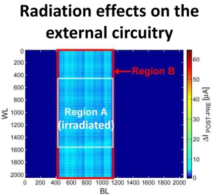
Radiation effects on the
external circuitry
(irradiated)
Devices belonging to the same WL or
BL are affected by radiation, even if
they do not lie in the irradiated region
Radiation effects on scaled PCM
Partial amorphisation due to the
temperature increase generated by
the heavy-ions impinging on the
active layer of 45 nm PCM
Radiation effect could impact the PCM depending on its device structure
Fig. 3 Color map of the value of the cells of a MOS-chip array irradiated with a
30 Mrad SiO2 proton beam. Region A is the irradiated zone and Region B is the area were the cells show a change in current of more than 1 A with respect to the pre-irradiation condition [3].
Fig. 4 Schematic of a phase change memory device hit by a heavy ion along
the word line [4].
Radiation effect on
chalcogenide materials
GST and Ge-rich GeSbTe (GGST)
1. As deposited (amorphous)
2. Annealed at 450°C (polycrystalline)
• 8.3 MeV/u Au
26+
-ions (E=1.635 GeV)
• Flux: 5E8 ions/cm
2
sec
Radiation effect on
4kb matrices
SET and RESET distribution
1. GST vs Ge-rich GeSbTe (w=100nm)
2. GST vs Interfacial Layer-PCM
(w=300nm)
• Fluences:
10E9, 5E10, 10E12, 5E12, 7E12,
1E13 ions/cm
2
• Fluences :
10E9, 5E10, 10E12 ions/cm
2
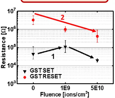
GST vs GGST
1. The SET state in GST faces a
structural relaxation at a fluence
of
10E9
ions/cm
2
plus
amorphisation at 5e10 ions/cm
2
2. The
GST
RESET
resistance
decreases with increasing fluence
1.
2.
2
Fig. 6 XRD patterns of GST crystalline layers before (REF) and after
irradiations at increasing fluence.
Fig. 7 TEM (left) and nano-diffraction patterns (right) analyses of as-deposited
amorphous GST after irradiation at a fluence of 1013ions/cm2.
Fig. 8 XRD patterns of GST amorphous layers before (REF) and after
irradiations at increasing fluence.
Fig. 5 Median and ±σ for SET and RESET distributions in GST 4kb arrays before
GST vs GGST
Fig 10 XRD patterns of GGST crystalline layers before (REF) and after irradiations at
increasing fluence.
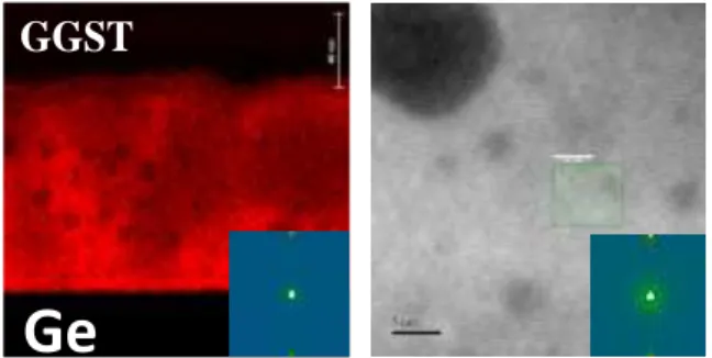
Fig 12 TEM/EDX and nano-diffraction patterns analyses of crystalline GGST after
irradiation at a fluence of 7 1012ions/cm2. The Ge cartography (left) shows that the
Ge segregation induced by the annealing process remains unchanged after irradiation. However, the irradiation reduces the size of the crystallites as evidenced by few and low intensity nano-diffraction patterns identified (right).
Fig. 9 Median and ±σ for SET and RESET distributions in GGST 4kb arrays before
and after irradiations at increasing fluences.
10
310
410
510
610
70
1E9
5E10
10
310
410
510
610
7Re
sis
tance
[
]
GGST SET
Re
sis
tance
[
]
Fluence [ions/cm
2]
GGST RESET
Fig 11 XRD patterns of GGST amorphous layers before (REF) and after irradiations at
increasing fluence.
GGST
Ge
SET and RESET states in GGST show
structural relaxation at both fluences
Both the resistance window and the
amorphous phase in the RESET state
are preserved making GGST more
stable than GST based devices thanks
to its higher T
c
0
1E9
5E10
10
110
210
310
410
510
610
70
1E9
5E10
10
110
210
310
410
510
610
70
1E9
5E10
10
110
210
310
410
510
610
70
1E9
5E10
10
110
210
310
410
510
610
7Fluence [ions/cm
2]
Re
sis
tance
[
]
GST RESET
Re
sis
tance
[
]
IL-PCM RESET
Re
sis
tance
[
]
IL-PCM SET
Re
sis
tance
[
]
GST SET
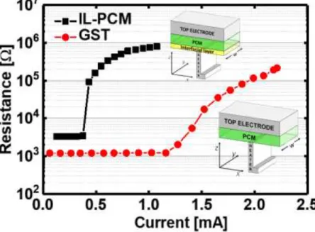
IL-PCM shows a higher radiation
tolerance due to the « smaller »
contact area between heater and
PCM
• Strong reduction in RESET current
for IL-PCM wrt GST
• The higher SET resistance in IL-PCM
is an evidence of the smaller
contact area created during the
programmig of the cell
GST vs IL-PCM
Fig. 13 Resistance-vs-Current characteristics comparing a standard GST device with
an IL-PCM. IL-PCM shows a high current reduction wrt GST in devices featuring same critical dimension (electrode area ~ 3 10-3µm2).
Fig. 14 Median and ±σ for SET and RESET distributions in GST and IL-PCM 4kb arrays
before and after irradiations at increasing fluences.
Fig. 15 Schematic of the zx-plane of an IL-PCM showing in red the