Publisher’s version / Version de l'éditeur:
Crystal Growth and Design, 8, 2, pp. 744-749, 2008-01-01
READ THESE TERMS AND CONDITIONS CAREFULLY BEFORE USING THIS WEBSITE. https://nrc-publications.canada.ca/eng/copyright
Vous avez des questions? Nous pouvons vous aider. Pour communiquer directement avec un auteur, consultez la première page de la revue dans laquelle son article a été publié afin de trouver ses coordonnées. Si vous n’arrivez pas à les repérer, communiquez avec nous à PublicationsArchive-ArchivesPublications@nrc-cnrc.gc.ca.
Questions? Contact the NRC Publications Archive team at
PublicationsArchive-ArchivesPublications@nrc-cnrc.gc.ca. If you wish to email the authors directly, please see the first page of the publication for their contact information.
NRC Publications Archive
Archives des publications du CNRC
This publication could be one of several versions: author’s original, accepted manuscript or the publisher’s version. / La version de cette publication peut être l’une des suivantes : la version prépublication de l’auteur, la version acceptée du manuscrit ou la version de l’éditeur.
For the publisher’s version, please access the DOI link below./ Pour consulter la version de l’éditeur, utilisez le lien DOI ci-dessous.
https://doi.org/10.1021/cg700816n
Access and use of this website and the material on it are subject to the Terms and Conditions set forth at
Growth of cookie-like Au/NiO nanoparticles in SiO2 sol-gel films and
their optical gas sensing properties
Buso, Dario; Guglielmi, Massimo; Martucci, Alessandro; Mattei, Giovanni;
Mazzoldi, Paolo; Sada, Cinzia; Post, Michael L.
https://publications-cnrc.canada.ca/fra/droits
L’accès à ce site Web et l’utilisation de son contenu sont assujettis aux conditions présentées dans le site LISEZ CES CONDITIONS ATTENTIVEMENT AVANT D’UTILISER CE SITE WEB.
NRC Publications Record / Notice d'Archives des publications de CNRC:
https://nrc-publications.canada.ca/eng/view/object/?id=91616577-e29b-4b9f-87dc-dbfacd986bb0 https://publications-cnrc.canada.ca/fra/voir/objet/?id=91616577-e29b-4b9f-87dc-dbfacd986bb0Growth of Cookie-like Au/NiO Nanoparticles in SiO
2Sol–Gel Films
and Their Optical Gas Sensing Properties
Dario Buso,†Massimo Guglielmi,†Alessandro Martucci,*,†Giovanni Mattei,‡ Paolo Mazzoldi,‡Cinzia Sada,‡and Michael L. Post§
Dipartimento di Ingegneria Meccanica - Settore Materiali, UniVersità di PadoVa,
Via Marzolo, 9, I-35131 PadoVa, Italy, Dipartimento di Fisica, UniVersità di PadoVa, Via Marzolo 8, I-35131 PadoVa, Italy, and Institute for Chemical Process and EnVironmental Technology, National Research Council of Canada, 1200 Montreal Road, Ottawa, Ontario K1A 0R6, Canada
ReceiVed August 28, 2007; ReVised Manuscript ReceiVed October 10, 2007
ABSTRACT: The favorable lattice matching between Au and NiO crystals made possible the growth of unique cookie-like nanoparticles (25 nm mean diameter) inside a porous SiO2 film by simply tailoring the film synthesis parameters. The unusual aggregates result from the coupling of well distinguishable Au and NiO hemispheres, which respectively face each other through the (100) and (200) lattice planes. High resolution transmission electron microscopy analysis revealed that the 2-fold nanostructures show a sharp flat interface with epitaxial coherence between the Au and NiO phases. The surface plasmon resonance (SPR) bands observed in optical absorption spectra provides evidence for the effect of the atypical dielectric nature of the media surrounding the Au aggregates. The films show noticeable and reversible change in the optical transmittance when exposed to CO and H2, with different features according to the detected species. The presence of CO does not modify the maximum SPR band wavelength, while H2induces a clear shift of the overall plasmonic resonance frequencies.
Introduction
The application of nanostructured materials in the design of new gas sensing devices is presently one of the most dynamic research issues, due to the possibility of increasing sensing performance by exploiting the high activity, large specific surface, and small size of sensor active materials.1Optical gas sensors can offer significant advantages in comparison to electric-conductometric devices in some circumstances. For instance, they display high immunity to electromagnetic noise, fire resistance, inactivity in flammable environments, and provide a capability of remote control and information transfer through optical fiber networks.2,3 Moreover, new potential applications in multigas detection can be achieved by exploiting differences in the intensity, wavelength, phase, and polarization of the output optical signal.4
Kobayashi et al.5first observed that thin films of NiO, Co3O4, and MnO3at temperatures around 250–350°C show reversible decreases in the visible-NIR absorption induced by CO. The absorbance change was associated with a decrease in positive hole density on the oxide surface during catalytic CO oxidation. Later, it was established that the introduction of small Au particles in the films enhanced the sensitivity toward the same gases6,7 or in some cases induced a sensitivity not observed otherwise.8
In previous work, we demonstrated that in comparison to undoped NiO, the optical gas sensing effect can be enhanced by the introduction of Au particles into a porous sol–gel silica matrix together with NiO nanocrystals.9It was also shown that the formation of a unique NiO/Au 2-fold nanoparticle structure existed in the matrix and that this intimately affects the optical gas sensing properties of the nanocomposite film.10The
objec-tives of this work are to show how the 2-fold NiO/Au cookie-like nanoparticles nucleate and evolve inside the silica matrix, and the resulting consequence of this type of structural morphol-ogy to the improvement of their optical gas sensing properties.
Experimental Section
The nanocomposite films were prepared by mixing a matrix silica solution containing the precursors for silica and gold, and a doping solution containing the precursor for NiO. The precursor solution for the silica matrix was made by mixing tetra-ethoxy silane (TEOS), methyl-triethoxy silane (MTES), H2O, HCl in EtOH according to molar
ratios TEOS/MTES/H2O/HCl/EtOH ) 1:1:4:0,02:4. HAuCl4·3H2O was
used as the metallic gold precursor, and this was added directly in the matrix solution according to a Ni/Au ) 5:1 molar ratio. The NiO precursor solution was made mixing NiCl2·6H2O in EtOH in the
presence of N-[3-(trimethoxysilyl)propyl]-ethylenediammine (DAEPT-MS) keeping the molar ratio of Ni/DAEPTMS ) 1. The double amminic groups of DAEPTMS coordinate the Ni2+ cations in the
solution, while the silanic group ensures the homogeneous dispersion of cations distributed inside the final SiO2network. A nominal SiO2/
NiO molar ratio of 3:2 has been used. The two precursor sols were then mixed together to obtain the final batch used for film growth.
Films were deposited on silicon or quartz glass substrates via the dip-coating technique using a withdrawing speed of 100 cm/min at 23
°C and controlled relative humidity (RH% ) 25%). Thermal annealing of the films was performed in air at 500, 600, and 700°C for 60 min. Infrared spectroscopy (FTIR) was performed in the 400–4000 cm-1
range using a Perkin-Elmer 2000 System instrument.
Structural and compositional characterization was performed at CNR-IMM (Bologna, Italy) on cross-sectional samples of the composite films. Measurements were taken with a field-emission FEI TECNAI F20 SuperTwin FEG-(S)TEM microscope operating at 200 kV and equipped with an EDAX energy-dispersive X-ray spectrometer (EDS) for compositional analysis and a Gatan 794 Multiple Scan Camera, allowing digital image recording on a 1024 × 1024 pixel CCD array. Scanning TEM (STEM) analysis coupled with EDS allowed compositional analysis on single clusters by means of line scans with an electron probe resolution of 1 nm fwhm.
All the films were characterized by X-ray diffraction (XRD) by using a Philips diffractometer equipped with glancing-incidence X-Ray optics. The analysis was performed at 0.5°incidence angle using CuKR
Ni-filtered radiation at 40 kV and 40 mA.
* To whom correspondence should be addressed. Tel.: 0039 0498275506. Fax: 0039 0498275505. E-mail: alex.martucci@unipd.it. Web: http://www. dim.unipd.it/martucci.
†Dipartimento di Ingegneria Meccanica - Settore Materiali, Università di
Padova.
‡Dipartimento di Fisica, Università di Padova. §National Research Council of Canada.
CRYSTAL
GROWTH
& DESIGN
2008
VOL. 8, NO. 2
744–749
10.1021/cg700816n CCC: $40.75 2008 American Chemical Society Published on Web 01/01/2008
SIMS measurements were carried out by means of an IMS 4f mass spectrometer (Cameca, Padova, Italy) using a 10 kV Cs+
primary beam and by negative secondary ion detection (the sample potential was fixed at -4.5 kV) with a final impact energy is 14.5 KeV. The SIMS spectra were obtained in ultra high vacuum conditions at a different primary beam intensity (15 nA) rastering over a nominally 125 × 125 µm2
area. The beam blanking mode was used to improve the depth resolution, by interrupting the sputtering process during magnet stabilization periods. The dependence of the erosion speed on the matrix composition was taken into account by measuring the erosion speed at various depths for each sample. The erosion speed was then evaluated by measuring the depth of the erosion crater at the end of each analysis by means of a Tencor Alpha Step profilometer with a maximum uncertainty of a few nanometers. The measurements were performed in high mass resolution configuration to avoid mass interference artifacts, and the charge build up while profiling the insulating samples was compensated by an electron gun without any need to cover the surface with a metal film.
Optical sensor functionality was studied by performing optical absorbance/transmittance measurements over the wavelength range 350 <λ < 850 nm with sample films mounted on a heater in a custom built gas flow cell. Transmission data were recorded with a Varian Cary1E spectrophotometer with films heated between 300–350°C and exposed to different concentrations of H2or CO in dry air at a flow
rate of about 0.4 L per min. The substrate size for these measurements was approximately 1 × 2 cm, and the incident spectrophotometer beam was normal to the film surface and covered a 6 × 1.5 mm2section
area.
Results and Discussion
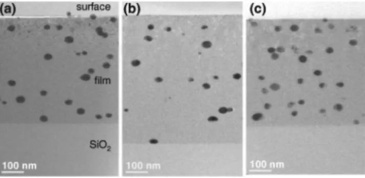
Bright-field (BFTEM), scanning (STEM), and high resolution transmission electron microscopy (HRTEM) were used to study the evolution of the structure of the nanocomposite films. Figure 1 presents the cross sectional bright-field transmission electron microscopy images of films annealed at different temperatures (500, 600, and 700°C) for constant time interval (60 min). The films exhibit a thickness in the 520–590 nm range with nanoclusters uniformly distributed.
The morphology of the sol–gel films heated at 500°C (Figure 1a) shows a composite with a thickness of 510 ( 10 nm containing Au nanoclusters of irregular and elongated shape. Two main populations of Au clusters are present: a minor one represented by spherical clusters with a size of about 5 nm, which is more densely distributed near the sample surface, and a second family of clusters with a size in the range of 25 nm and with a more elongated shape. Statistically, the major axis of the elongated particles lies parallel to the film surface. The nanocluster size (averaged over the two main axes) for this second population is <D> ) 25.7 ( 6.6 nm (average diameter (standard deviation of the experimental size distribution). The same morphology is found upon annealing at 600°C (Figure 1b) and 700°C (Figure 1c): the main difference with the sample annealed at 500°C is the presence of more complex morphology of the nanoclusters: some of them exhibit a 2-fold structure in which a part with a brighter contrast is attached to the Au nanoparticles. In particular, in the films heated at 600°C the population of the small Au clusters close to the surface of the film starts to disappear, while in the film bulk, larger Au clusters are present together with some having a partially formed 2-fold structure (Figure 1b). This dissolution is complete in the sample annealed at 700°C. Figure 1c shows that from the morphologi-cal point of view this sample shows further development of the 2-fold cluster structure, with a size that is increased with respect to those in the film annealed at lower temperatures: the nanocluster size (averaged over the two main axes) is <D> ) 31.2 ( 9.6 nm. A further feature that starts to develop under 600–700°C annealing is a residual porosity at the sample surface probably induced by the dissolution of the smallest Au nanoclusters.
To better investigate the nature of the contrast variation in the nanoclusters, an STEM analysis of the systems was performed. The STEM signal collected with a high-angle annular dark field detector (HAADF) from a representative part of the film annealed at 500°C is shown in Figure 2a. The brighter contrast in the image indicates that the particles were constituted from the heavier element (Au in this case). From the image, it is evident that most of the smallest clusters produce a bright contrast, therefore indicating that they are composed of Au. Selected area electron diffraction (SAED) on the film showed (Figure 2b) that along with the Au fcc reflections (aAu)0.4079 nm) the diffraction peaks corresponding to the crystalline NiO cubic phase (aNiO) 0.4177 nm) are also present. The small differences between the reflections in the two cubic structures are shown in Figure 2c. This result has been confirmed by a detailed HRTEM analysis. Figure 3a indicates that at 500°C near the Au clusters, showing the lattice fringes corresponding to the (111) lattice planes, some NiO particles are grown, with Figure 1. Cross sectional BFTEM image of the film annealed at
500°C (a), 600°C (b), and 700°C (c).
Figure 2.TEM results on the film annealed at 500°C: (a) STEM-HAADF cross sectional image; (b) SAED electron diffraction; (c) theoretical diffraction intensities of the bulk cubic Au and NiO crystalline phases.
the (200) planes clearly visible, and with a size of about 5 nm. This demonstrates that at 500°C nucleation and growth of a NiO separated crystalline phase has taken place. This is also confirmed by compositional EDS-STEM analysis on both clusters in Figure 3a: no Au EDS signal is obtained when focusing the beam onto the cluster giving NiO (200) lattice fringes, whereas it is dominant when focusing on the other cluster.
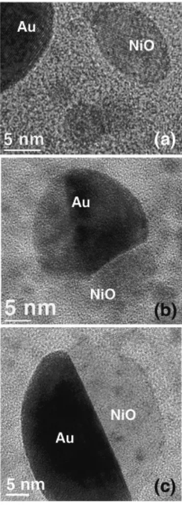
A comparison of the Au-NiO nanostructure in the films annealed at the three temperatures is shown in Figure 3: with respect to the film annealed at 500°C in which separated Au and NiO clusters are present, the samples annealed at 600°C (Figure 3b) and at 700°C (Figure 3c) exhibit the 2-fold structure, which from the HRTEM and STEM+EDS analyses can be described as being constituted of both Au and NiO arranged in a cookie-like structure,10with the (111) planes of Au parallel to the (200) ones of the NiO phase.
Figure 3.HRTEM results on the films annealed at (a) 500°C, showing separated Au and NiO nanoclusters; (b) at 600°C with one growing cookie-like NiO/Au cluster; and (c) 700°C with a fully grown cookie-like NiO/Au cluster.
Figure 4.XRD spectra of nanocomposite films annealed at 500, 600, and 700°C. The main diffraction intensities lines of cubic NiO (PDF #471049) and Au (PDF #40784) are reported on the bottom.
Figure 5.SIMS data of film annealed at 700°C showing depth profile of O, Si, Ni, and Au species.
The STEM-EDS compositional analysis of the matrix around the clusters indicates a mixture of amorphous SiO2and NiO for all the samples with the Si/Ni atomic ratio increasing with the annealing temperature.
XRD measurements (see Figure 4) confirmed the presence of both NiO (bunsenite, PDF #471049) and Au (PDF #40784) crystalline phases in all the nanocomposite films. As shown in the figure, the NiO diffraction peaks become better resolved following an increase in the annealing temperature, confirming the evolution of NiO crystal growth observed by HRTEM.
The evolution of the nanostructure could be interpreted in terms of growth of the Au clusters either in a diffusion-limited regime, sustained by possible Au atoms dispersed in the matrix, or in the Ostwald ripening regime due to the Gibbs–Thomson effect.11,12Indeed, it has been already demonstrated12that Au atoms diffuse readily in SiO2at temperatures equal to, or higher than, 600 °C in an oxygen containing atmosphere. The Au nanocluster growth is coupled with the parallel nucleation of the NiO crystalline phase, which probably tends to use the Au (111) planes as a structural template for nucleating the growth, therefore forming the double structured cookie-like Au/NiO clusters found in the 600°C and more distinctly in the 700°C annealed sample. The phase separation between SiO2and NiO in the matrix with the progressive formation of the cookie-like structure is also demonstrated by the increasing of the Si/Ni atomic ratio in the matrix surrounding the nanoclusters as measured by EDS. XRD measurements further confirm that the NiO crystallization increases by increasing the annealing temperature.
The SIMS data reported in Figure 5 for the film heated at 700°C demonstrate that all the species (Si, O, Ni, and Au) are uniformly distributed through the whole film thickness, the film-to-substrate interface being sharp. Similar results are obtained for the two other temperatures, indicating that, within the experimental error, the content of Au does not vary with the heat treatment, and that no migration of gold toward the surface is found.
FTIR analysis was used to qualitatively describe the main features of the SiO2matrix. Figure 6 reports FTIR spectra of the films annealed at different temperatures. The main peak centered in the 1060–1080 cm-1
range is associated with antisymmetric stretching vibrations (TO3modes) of Si-O bonds in Si-O-Si groups inside the SiO2network,13while the wide shoulder centered around 1200 cm-1 is attributed to LO
3 stretching modes of Si-O-Si bonds, activated by scattered IR radiation within the pore walls.13 Peaks at 816 cm-1 are attributed to symmetric stretching (or bending14) motion (TO
2) of oxygen atoms in Si-O-Si bonds.13Signals at 960 and 1648 cm-1
can be attributed to stretching of nonbridging oxygen
atoms (for example, unreacted Si-OH groups)14 and weak bending vibration of H-O-H in H2O,15respectively. Densi-fication of the SiO2network induced by thermal annealing can be monitored by recording the position of the main Si-O-Si vibration signal,16and by this means obtain a relative scale of film porosity. A peak maximum frequency shift from 1072 to 1078 cm-1is observed for films annealed at 500 and 700°C, respectively, which can be explained by an increase of matrix densification induced by the heat treatment.
Figure 7 shows the optical absorption spectra of the films heated at different annealing temperatures. The films appear transparent and with a color ranging from red (film annealed at 500°C) to blue (film annealed at 700°C). In fact the absorbance in the visible range of the samples is dominated by a strong Figure 7. Absorption spectra of films annealed at 500, 600, and
700°C.
Figure 8.Absorption spectra of film annealed at 500, 600, and 700°C when exposed to air (black solid line), to 1% H2(light gray solid line),
and to 1% CO (dotted line) at an operating temperature of 300°C.
band that red-shifts and changes form with heat treatment (see Figure 7). The film annealed at 500°C shows a band at 560 nm that is associated with the surface plasmon resonance (SPR) of conduction electrons on the surface of gold clusters, as observed to be present in the TEM data (Figure 1a). However, the absorption spectrum of the film annealed at 700°C exhibits two main bands; the most intense band is centered at 615 nm, and the other is present as a shoulder at about 530 nm. These bands are due to the 2-fold structure of the Au/NiO nanoparticles shown in Figure 3c. In support of this explanation, it has already been demonstrated10that the most intense absorption band is controlled by dielectric coupling at the Au-NiO interface, which red-shifts the position of the gold SPR band, while the SPR band at 530 nm is controlled by dielectric coupling at the Au-SiO2interface of the cookie-like nanoclusters. The film annealed at 600°C displays a broad absorption band centered at 575 nm reflecting the intermediate morphology depicted in the TEM image (Figure 3b).
The gas sensing functionalities of the nanocomposite films were tested by measuring the variation of the optical absorption in the presence of CO and H2.
The nanocomposite films exhibited clear and reversible absorbance changes in the visible-NIR wavelength region when exposed to CO or H2. Plots reported in Figure 8 summarize the absorbance variation registered for the films annealed at 500, 600, and 700°C, which show a strong discontinuity in the SPR band frequencies (500-650 nm), with opposite characteristics depending on the gas species. Upon exposure to CO, there is a decrease in absorbance over the whole wavelength range with the exception of wavelengths near the plasmon absorption band, while for H2 there is a change in shape and position of the plasmon band. These features can be better appreciated con-sidering the data showing the optical absorbance change ratio (ACR) defined as (Absair-Abs1%CO)/Absair(see Figure 9). This definition, with a normalizing factor of Absair, was chosen to accommodate any differences in the transmitted optical signal that could arise from inhomogeneities in film thickness, unequal reflectance ratios of the measuring beam, and calibration discrepancies that otherwise could lead to misleading compari-son of data.
The changes in absorbance clearly display a dependence in magnitude and sign of ACR with respect to wavelength for both gases. Thus, in the region of the SPR band, CO induces a clear depression in ACR, which is maximized for the film heated at 700°C, for which there is a larger reversal of sign of the ACR in comparison with the sample heated at 500°C. H2induces a blue shift of the plasmon band and positive variation of the ACR, which is maximized for the film heated at 500°C.
In NiO films that have no noble metal component, the decrease in absorbance is close to constant in the 350–850 nm wavelength range and is ascribed to a decrease in positive hole density of NiO during the catalytic oxidation of CO or H2.4 Thus, for the present case with NiO and Au nanoparticles, at wavelengths outside the plasmon band the decrease in absor-bance observed for CO can be ascribed to the same mechanism. The mechanism for the absorbance increase in the plasmon band is, however, not determined yet,17but it is clearly associated with the interaction of CO with the Au/NiO interfaces. On the other hand, the variation in absorbance due to H2 is rather different and cannot be explained with the same mechanism. To explain the influence of gold nanoparticles on the reducing gases detection mechanism of transition metal oxides, two types of effects have been proposed.18Type 1 is related to an increased catalytic activity promoted by gold, closely associated with the catalytic activity of the Au-transition metal oxide composite.19 In Type 2, the enhancement arises from the plasmon absorption change of Au particles, and it is not directly related to the catalytic oxidation. SPR frequencies are strongly influenced by Figure 9.Optical absorbance change ratio (Absair-Absgas)/Absairof film annealed at 500, 600, and 700°C at an operating temperature of 300°C
for 1% CO (a) and for 1% H2(b).
Figure 10.(a) Temporal response of film annealed at 700°C to different concentration of CO (a ) 10, b ) 100, c ) 1000, d ) 10000 ppm). Measurements made at l ) 690 nm and at an operating temperature of 330°C. (b) log of relative response (TrCO/TrAir) versus log of gas concentration.
the physical properties of the surrounding material, such as dielectric constants. A gas induced variation of these properties would affect both wavelength and shape of the SPR band of gold particles, as already observed in Au-CuO4,18 films when exposed to CO. In the present case, the type 2 effect can be excluded for CO, because the SPR band of the nanocomposite film is not appreciably modified by 1% v/v CO for either wavelength or band shape (Figures 8 and 9a). On the contrary for H2the type 2 effect is the most probable, because both the shape and the position of SPR change (Figures 8 and 9b), in contrast with observations summarized by Ando et al. for NiO-Au systems.18
The H2detection mechanism is perhaps specific to the system Au-NiO described here, as studies determining the H2effects upon optical properties of other Au-metal oxides systems, such as Au-Co3O4,4,17Au-WO3,20and Au-InxOyNz,21report that H2 exposure causes an increase of optical absorption in SPR frequencies together with no substantial change in SPR band maximum wavelength, with the exception of a slight shift described in ref 21.
Further studies are in progress to better understand the different behavior shown by the NiO-Au nanocomposite films when exposed to CO and H2, but the differences measured for the two gases could allow multiple gas detection by wavelength selection.
To evaluate the sensor sensitivity, the films have been exposed to different concentrations of CO and H2. The films gave detectable responses in dynamic tests with a minimum concen-tration of 10 ppm (0.001% v/v) of both H2 and CO. As an example, Figure 10a shows the relative response (defined as the ratio of transmittance in CO, TrCO, to that in air, Trair) obtained at λ ) 690 for a film heat treated at 700 °C at an operating temperature of 330°C for four CO concentrations in air (10, 100, 1000, and 10000 ppm). Clearly a CO concentration dependence is evident, and transmittance changes are easily observable even at concentrations of 10 ppm CO. The form of the transmittance steps shows a good signal reversibility (i.e., recovery of the signal baseline after a change of CO concentra-tion) in the case of high CO concentrations, while at lower gas concentrations the exponential baseline recovery takes a longer time. Response time and recovery time are in any case on the order of 2–3 min. By plotting the relative response and gas concentration logarithmically, the relationship is linear as shown in Figure 10b. It is therefore clear that the films possess a higher linear sensitivity of the transmittance response at the lower CO concentrations. The present data demonstrate that CO levels of 10 ppm are easily detected, and the potential for detecting concentrations at even lower levels exists.
Conclusions
SiO2films doped with NiO and Au nanoparticles have been synthesized by the sol–gel technique. Tailoring the annealing
conditions of the dip-coated films leads to a controlled evolution of nanoparticle morphology in the porous SiO2matrix. HRTEM and STEM+EDS analyses showed that at 500°C the NiO and Au nanoparticles are separated while at 700°C the nanoparticles have a 2-fold structure formed by two hemispheres of NiO and Au arranged in a cookie-like structure, with the Au(111) planes parallel to NiO(200). The nanocomposite films showed new optical gas sensing behavior for the detection of CO and H2. Optical transmittance modulation was wavelength dependent with different features for the two gases. In the wavelength regions close to the Au-SPR band, a suppressed or reversed transmittance response was found during CO exposure, while H2showed an increase of optical transmittance with a transmit-tance variation up to 5 times larger than CO.
Acknowledgment. This work was supported by MURST within a “Progetto di Ateneo n. CPDA042175” Project of the Padova University.
References
(1) Shi, J.; Zhu, Y.; Zhang, X.; Baeyens, W. R. G.; García-Campaña, A. M. TrAC, Trends Anal. Chem. 2004, 23, 1.
(2) Educhi, K. In Gas Sensors; Sberveglieri, G. Ed.; Kluwer Academics Publishers: Dordrecht, 1992; p 307.
(3) Seiz, W. R. Anal. Chem. 1984, 56, 16A.
(4) Ando, M.; Kobayashi, T.; Haruta, M. Catal. Today 1997, 36, 135. (5) Kobayashi T.; Haruta M.; Sano H.; Delmon B. Proceedings of the
Third International Meeting on Chemical Sensors, Cleveland, Ohio, September 23-26, 1990; p 318.
(6) Kobayashi, T.; Haruta, M.; Ando, M. Sens. Actuators, B 1993, 13–
14, 545.
(7) Ando, M. Kobayashi T., Haruta M. J. Chem. Soc. Faraday Trans.
1994, 90, 1011.
(8) Ando M.; Kobayashi T.; Haruta M. Sens. Actuators, B 1995, 24–25, 851.
(9) Buso, D.; Guglielmi, M.; Martucci, A.; Mattei, G.; Mazzoldi, P.; Sada, C.; Post, M. L. Nanotechnology 2006, 17, 2429.
(10) Mattei, G.; Mazzoldi, P.; Post, M. L.; Buso, D.; Guglielmi, M.; Martucci, A. AdV. Mater. 2007, 19, 561.
(11) De Marchi, G.; Mattei, G.; Mazzoldi, P.; Sada, C.; Miotello, A. J. Appl.
Phys. 2002, 92, 4249.
(12) Miotello, A.; De Marchi, G.; Mattei, G.; Mazzoldi, P.; Sada, C. Phys.
ReV. B 2001, 63, 075409-(1-6).
(13) Almeida, R. M.; Pantano, C. G. J. Appl. Phys. 1990, 68, 4225. (14) Primeau, N.; Vautey, C.; Langlet, M. Thin Solid Films 1997, 310, 47. (15) Vallée, C.; Goullet, A.; Granire, A.; van der Lee, A.; Durand, J.;
Marlière, C. J. Non-Cryst. Solids 2000, 272, 163. (16) Galeener, F. G. Phys. ReV. B 1979, 19, 4292.
(17) Ando, M.; Kobayashi, T.; Iijima, S.; Haruta, M. J. Mater. Chem. 1997,
7, 1779.
(18) Ando, M.; Kobayashi, T.; Iijima, S.; Haruta, M. Sens. Actuators, B
2003, 96, 589.
(19) Haruta, M.; Yamada, N.; Kobayashi, T.; Iijima, S. J. Catal. 1989,
115, 301.
(20) Ando, M.; Chabicovsky, R.; Haruta, M. Sens. Actuators, B 2001, 76, 13.
(21) Ando, M.; Steffes, H.; Chabicovsky, R.; Haruta, M.; Stangl, G. IEEE
Sens. J. 2004, 40-2, 232. CG700816N