HAL Id: hal-01887362
https://hal-univ-paris.archives-ouvertes.fr/hal-01887362
Submitted on 10 Oct 2018
HAL is a multi-disciplinary open access
archive for the deposit and dissemination of
sci-entific research documents, whether they are
pub-lished or not. The documents may come from
teaching and research institutions in France or
abroad, or from public or private research centers.
L’archive ouverte pluridisciplinaire HAL, est
destinée au dépôt et à la diffusion de documents
scientifiques de niveau recherche, publiés ou non,
émanant des établissements d’enseignement et de
recherche français ou étrangers, des laboratoires
publics ou privés.
organic junctions based on aryl thin films covalently
attached to a multilayer graphene electrode
Clement Barraud, Matthieu Lemaitre, Roméo Bonnet, Jacko Rastikian, Chloé
Salhani, Stéphanie Lau, Quyen van Nguyen, Philippe Decorse,
Jean-Christophe Lacroix, Maria Luisa Della Rocca, et al.
To cite this version:
Clement Barraud, Matthieu Lemaitre, Roméo Bonnet, Jacko Rastikian, Chloé Salhani, et al.. Charge
injection and transport properties of large area organic junctions based on aryl thin films
cova-lently attached to a multilayer graphene electrode. Nanoscale Advances, RSC, 2018, 00, pp.2 - 8.
�10.1039/C8NA00106E�. �hal-01887362�
Nanoscale
ARTICLE
a.MPQ UMR 7162, Université Paris Diderot, Sorbonne Paris Cité, CNRS, F-75013
Paris, France.
b.
ITODYS UMR 7086, Université Paris Diderot, Sorbonne Paris Cité, CNRS, F-75013 Paris, France.
c. Department of Advanced Materials Science and Nanotechnology, University of
Science and Technology of Hanoi, Vietnam Academy of Science and Technology, 18 Hoang Quoc Viet, Cau Giay, Hanoi, Vietnam.
See DOI: 10.1039/x0xx00000x Received 00th January 20xx, Accepted 00th January 20xx DOI: 10.1039/x0xx00000x
www.rsc.org/
Charge injection and transport properties of large area organic
junctions based on aryl thin films covalently attached to a
multilayer graphene electrode
Clément Barraud*a, Matthieu Lemaitrea, Roméo Bonneta, Jacko Rastikiana, Chloé Salhania,
Stéphanie Laub, Quyen Van Nguyenb,c, Philippe Decorseb, Jean-Christophe Lacroixb, Maria Luisa
Della Roccaa, Philippe Lafargea and Pascal Martin*b
The quantum interaction between molecules and electrode’s material at molecules/electrode interfaces is a major ingredient in the electronic transport properties of organic junctions. Driven by the coupling strength between the two materials, it results mainly in a broadening and an energy shift of the interacting molecular orbitals. Using new electrodes materials, such as the recent semi-conducting two-dimensional nanomaterials, has become a recent challenge in the field of molecular/organic electronics that opens new possibilities for controlling the interfacial electronic properties and thus the charge injection properties. In this article, we report the use of atomically thin two-dimensional multilayer graphene films as base electrode in organic junctions with a vertical architecture. The interfacial electronic structure dominated by the covalent bonding between bis-thienyl benzene diazonium-based molecules and the multilayer graphene electrode has been probed by ultraviolet photoelectron spectroscopy and the results compared with those obtained on junctions with standard Au electrodes. Room temperature injection properties of such interfaces have been also explored by electronic transport measurements. We find that, despite strong variations of the density of states, the Fermi energy and the injection barriers, both organic junctions with Au base electrodes and multilayer graphene base electrodes show similar electronic responses. We explain this observation by the strong orbital coupling occurring at the bottom electrode/ bis-thienyl benzene molecules interface and by the pinning of the hybridized molecular orbitals.
1. Introduction
The architecture of the two- and three-terminals building
blocks of organic electronic devices, such as
electroluminescent diodes and organic transistors, is largely inspired by their inorganic counterparts. Practically, the control and understanding of the electrode/molecules interface’s properties is crucial for reaching high performances
and designing functionalities1, such as electrical rectification.
Symmetric current density as a function of bias voltage (J-V) characteristics were widely observed in two-terminal devices
and discussed in the case of single molecule junctions2,
monolayers3 or oligomers based-organic junctions, as in the
case of a large variety of aromatic nanostructures between
conducting carbon electrodes4,5. It has been shown that to
introduce asymmetry (rectification) in the electronic response
of molecular and organic junctions, it is necessary to introduce
an asymmetry along the transport direction6,7. This can be
achieve either by using different contact electrodes (i.e. with different injection properties), and/or by using asymmetric anchoring moieties or molecular structures as originally
proposed by Aviram and Ratner8. Using such artificial systems
to create nano-rectifiers has been widely reported and
recently reviewed9. The electrode/molecules coupling plays
also a crucial role in defining the amplitude of the rectification
ratio (RR)9. Molecules can be either attached to electrodes via
strong (chemisorption) or weak interactions (physisorption). Depending on the nature of the interactions on both sides of the junctions, the RR has been demonstrated to vary from few
tenth to few thousands9. Recently record RR up to 105 were
reported in alkyl-ferrocene-based self-assembled monolayers contacted by chemisorption to a bottom electrode and
physisorption to a top electrode10. The rectification effect was
also shown to be strongly dependent upon the position of the Fc unit (i.e. the molecular structure) between the two
electrodes11. We have shown before that based on diazonium
approach oligo-BTB form high quality organic layer and lead to
highly stable organic junctions.5,12 We have reported molecular
diodes based on diazonium grafting in junctions of the form of Au-BTB//Ti/Au where “-” and “//” denote the bottom interface
ARTICLE Journal Name
and the top interface respectively.13 Those organic diodes
presented large rectification ratio RR of 1000 and we clearly demonstrated that the rectification behaviour in this configuration is an evidence of molecular signature even if the two metallic electrodes have different Fermi energies. Several molecules have been tested into junctions and the RR varied
from 10-2 to 103 with a very good reproducibility and same
conditions.
In this article, we focus on the electrode’s properties. New atomically thin electrodes made of two-dimensional materials, such as graphene, have been recently proposed and developed
to replace more traditional metallic electrodes14 more
sensitive to oxidation and/or electro-migration. Graphene, multilayer graphene (MG) and graphite were recently used as a soft, transparent and tunable electrode for contacting
rubrene single crystals15, self-assembled monolayers16–18 and
even single molecules19–24. The strength of the chemical
bonding between a graphene/graphite electrode and molecules was demonstrated to be a key ingredient over the
global electronic response of single-molecule junctions23.
Here we demonstrate electrical rectification effects in the case of MG-(oligo(1-(2-bisthienyl) benzene, named BTB) diazonium-based thin film//Ti/Au junctions. We show that rectification is directly linked to the strong orbitals coupling at the MG-BTB
interface like in the well-studied case of Au-BTB interfaces12
and to pinning of the hybridized molecular orbitals at top and bottom electrode/molecules interfaces. Our observation is strongly supported by a comparative analysis of those two device’s interfaces by electronic transport measurements and ultraviolet photoelectron spectroscopy.
2. Experimental section
Multilayer graphene transferMG was purchased on Ni films. The Ni/MG bilayer was first covered with a thin layer of PMMA 950K deposited by spin-coating (4000 rpm) and baked at 110°C for 10 minutes. The Ni/MG/PMMA trilayer was then gently deposited at the
surface of a FeCl3 bath in order to dissolve the Ni substrate.
After dissolution, the floating MG/PMMA bilayer was
transferred in a deionized H2O bath for 5 minutes. MG was
cleaned in successive baths following the recipe described in
reference 25 (i.e. RCA clean). It was then transferred in a
deionized H2O bath and then gently “fished” by the substrate.
After transfer, the sample was slowly baked from room temperature to 110°C in order to evaporate the remaining water. The PMMA film was finally removed by immersing the sample in a warm (50°C) acetone bath for 5 minutes and in an isopropanol bath for 2 minutes.
Electro-grafting
The 1-(2-bisthienyl)-4-aminobenzene (BTB) was synthesized
following a published procedure26. For electrochemical
experiments, a conventional one-compartment, three-electrode cell was employed. A CHi 760C potentiostat (CH Instruments, Austin, TX) was used. The auxiliary electrode was
a platinum grid. A SCE (3 M KCl) in an ACN/LiClO4 bridge was
used as a reference electrode. Experimental setup
DC electrical measurements were performed by applying a DC voltage signal to the junction top electrode by a low-noise voltage source (Yokogawa GS200). The output current was measured by a low-noise current-voltage amplifier connected to the bottom electrode. The amplified output was measured by a digital voltmeter (Agilent 34405A).
Spectroscopy characterizations
XPS and UPS analyses were performed in ultrahigh vacuum system (VG Scientific ESCALAB 250) with a base pressure of
2.10-10 mbar. XPS was performed using an Al KR X-ray source
(1486.6 eV) and a microfocused monochromatic and magnetic lens. The spectra were acquired in the constant analyzer energy mode with pass energies of 150 and 40 eV for the survey and the narrow regions, respectively. UPS was carried out using monochromatic He I (21.21 eV) emission together with a toroidal mirror monochromator.
Yield and reproducibility
A high percentage (80 %) of working and reproducible devices is found in the case of Au-BTB//Ti/Au junctions in agreement
with previous reports13. The yield of working devices is
reduced when MG is inserted (around 20 %). It may be explained by the relatively high peak-to-peak roughness (< 10 nm) due to folds of the MG electrode compared to a more standard evaporated Au electrode (< 1 nm) as revealed by the AFM image presented in the figure 1(c). All the J-V characteristics presented are stable over periods of several hours.
3. Results and discussion
MG-BTB//Ti/Au junctions were fabricated by first transferring a MG layer (purchased from Graphene Supermarket®) over an
insulating 280 nm SiO2 substrate. The transfer technique is
adapted from Ref. 25 and is described in the experimental
section. Two Raman spectra acquired on MG after transfer (laser wavelength: 633 nm) in two different locations are shown in figure 1(a), together with an optical microscope
image (inset of figure 1(a)) of a 500 nm SiO2 substrate covered
by the transferred MG. The observed changes in the shape and relative heights and widths of the G and 2D peaks reveal that the number of graphene layers is not uniform over the entire
MG film27. This is expected as the MG thickness is specified
from Graphene Supermarket® to be equal to 4 monolayers in average with local variations between 1 and 7 monolayers. The absence (black line) or the weak (red line) D peak arising
around 1350 cm-1 confirms the excellent structural quality of
the MG after transfer. The MG is then patterned by optical
lithography and O2 plasma (70 W during 120 s) in long stripes
Figure 1: (a) Two Raman spectra acquired at different locations on MG after transfer on a 280 nm SiO2 substrate (laser wavelength: 633 nm). Inset: optical image of a MG film
deposited over a 500 nm SiO2 substrate. (b) Cyclic voltammograms of
(1-(2-bisthienyl)-4-aminobenzene) (BTAB) electro-reduction in acetonitrile (10 cycles at 0.1 V.s-1) over
the MG electrode. Inset: molecular structure of the BTB molecule. (c) Atomic force microscopy topography image of a MG grafted with BTB molecules acquired in ambient conditions in tapping mode (10 x 10 µm2) (d) Raman spectrum acquired on MG/BTB
surfaces highlighting the region between 1000 cm-1 and 1550 cm-1 where the resonances associated to the oligo(BTB) molecules are observed. Inset: Raman spectrum acquired on a high-purity 1-(2-bisthienyl) benzene amine powder revealing similar resonances.
After fabrication of the patterned MG electrodes,
electrochemical grafting of BTB was carried out in solution by cyclic voltammetry. Figure 1(b) shows a cyclic voltammetry characteristic of the reduction of the 1-(2-bisthienyl) benzene diazonium cation at the surface of a MG electrode. It shows an irreversible wave during the first scan [+0.4 V; -0.4 V], which
corresponds to the formation of aryl radicals28 at the proximity
of the MG electrode. In the following scans, the current strongly drops to zero as the conducting surface of the electrode becomes passivated by the growth of an oligo-BTB
thin layer26. BTB thin films are electro-active and can be easily
p-doped at a potential close to 0.5 V/SCE (saturated calomel
electrode)26. As a consequence, the conductance of a BTB thin
film can be switched and diode-like behavior with a high rectification ratio is observed in the electrochemical response
of outer-sphere redox probes29. At the end of the process, the
MG surface is fully covered by the organic film as previously
detailed for graphene and graphite surfaces30. No trace of
diazonium salt was detected by X-ray photoelectron spectrometry analysis within the resolution of the detector (not shown). The final thickness and roughness of the BTB film were determined by atomic force microscopy as shown in figure 1(c) and was found to be around 10 ± 1 nm. After electro-grafting, the MG electrode was again characterized by Raman spectroscopy. Figure 1(d) shows the Raman spectrum (laser wavelength: 633 nm) acquired on the MG/BTB surface. While the main features from the graphitic structure, the D, G and 2D resonances, can still be identified, additional resonances (individually marked with colored *) are observed
in the frequency range 1000 cm-1 and 1550 cm-1. They are
attributed to vibrational modes (stretching vibration for C=C
aromatics (1520 cm-1 and 1450 cm-1) and C-H aromatics (1060
cm-1, 1140 cm-1 and 1180 cm-1)) within the oligo-BTB film31,32.
This is further probed by measuring the Raman spectrum of high-purity 1-(2-bisthienyl) benzene amine powder (inset of figure 1(d)), where clearly resonances at identical frequencies
are observed. In the Raman spectra of figure 1(d), the sp2
graphitic structure are still evident as only the topmost layer of
MG is chemically functionalized30 leaving the remaining layer
of the MG structure intact. The topmost layer is sp3 hybridized
giving rise to the increase of the visibility of the D peak around
1350 cm-1. This result is confirmed by measuring the resistance
(not shown) of a 2.5 mm long - 40 µm wide functionalized MG stripe. A value of ~25 kΩ is extracted in good agreements with
standard electrical characterizations of MG layers33. The top
electrode is finally patterned in cross-bar geometry by optical lithography. A thin film of Ti (1 nm)/Au (50 nm) is then
evaporated at pressure < 10-7 mBar and with low rate < 0.1
nm/s leading to the MG-BTB//Ti/Au organic/inorganic heterostructures without titanium oxide formation. As we
shown previously4,12,13,34–36, such organic layer was sufficiently
robust to allow the direct evaporation of metallic atoms. The titanium layer acts as an adhesion layer for gold evaporation but also as a blocking layer to avoid gold atom diffusion through the organic layer.
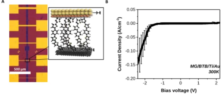
Figure 2: (a) Optical image of MG-BTB//Ti/Au junctions with various dimensions of junctions. A schematic view of a polarized junction is presented in the black box. (b) Average J-V characteristic measured at room temperature as a function of bias voltage characteristics for MG-BTB//Ti/Au junctions with standard deviation (over five characterized devices). Dimensions of the measured junctions were ranging from 5 x 40 µm2 to 20 x 40 µm2.
An optical image of the devices accompanied by a schematic of a polarized junction is depicted in figure 2(a). All the junctions
were electrically characterized using standard DC
measurement techniques. Details about the experimental setup can be found in the experimental section. Room temperature J-V characteristics for five different
MG-BTB//Ti/Au junctions with area ranging from 5 x 40 µm2 to 20 x
40 µm2 are plotted in figure 2(b). A rectifying effect is revealed
with a rectification ratio RR = |J(-2 V)/J(+2 V)| up to 100. The current density in the conducting states at negative voltages (i.e. current flowing from the bottom electrode to the top
electrode) reaches values up to 0.15 A cm2.
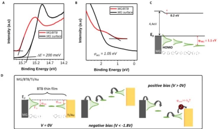
To gain insights on the electronic properties of the different
hybrid interfaces, we have performed ultraviolet
photoelectron spectroscopy (UPS) of a bare MG surface and of a MG-BTB interface. As mentioned already, BTB molecules are known to be p-type molecules and transport occurs
preferentially through the occupied molecular orbitals4,12. For
1500 2500 D 2D Int ens ity (a. u.) Raman shift (cm-1) G MG on SiO2 -0.4 -0.2 0.0 0.2 0.4 -1.0 -0.8 -0.6 -0.4 -0.2 0.0 Current (µA) Applied potential (V) BTB on MG C A 1000 1500 2500 BTB powder BTB on MG Si D G Intens ity (a. u.) Raman shift (cm-1 ) 2D BTB molecules 1000 1500 C-H in aromatics ** * * * * * * * Inte ns ity (a . u.) Raman shift (cm-1 ) * C=C in aromatics D B 50 µm 2 µm 0 nm 40 nm A B 500 µm -2 -1 0 1 2 -0.20 -0.15 -0.10 -0.05 0.00 0.05 Current Densit y (A/cm -2) Bias voltage (V) MG/BTB/Ti/Au 300K
ARTICLE Journal Name
UPS spectroscopy the MG-BTB bilayer was fabricated following the same procedure with a thinner BTB thickness (3-4 nm) in order to get relevant information for the injection barrier. The secondary electron cut-off and valence band spectra for MG (black line) and for MG-BTB (red line) are represented in figures 3(a) and 3(b) respectively. The very small density of states at the Fermi energy of MG gives the observed rather weak increase of the signal towards higher binding energies
compared to standard metals37. From these measurements,
we can extract the vacuum level shift (E = 0.2 eV), generally
interpreted as the presence of dipoles at the
electrode/molecules interfaces38 and the injection barrier 3-4
nm away from the interface (MG = 1.1 eV). Both values of
vacuum level shift and injection barrier are comparable with reported values of BTB and other diazonium compounds
grafted on pyrolized photoresist film by Sayed et al.4 The
extracted work function WF of MG surface was 4.4 eV
consistent with the literature39–41 and was found to be very
close to the WF of a Ti surface (4.3 eV)42, the top electrode of
our devices. These values are reported on the energy diagram of the MG-BTB interface presented in figure 3(c). First the value of WF indicates that the two electrodes are at the same energy level at 0 V. In such case, without taking into account the coupling at the interfaces, we should expect symmetric J-V characteristics and no rectification appears. However the rectification observed indicates that the coupling at both interfaces is different and we attempt to explain this behaviour in the following. The first molecular monolayer is expected to be strongly coupled to MG and molecular orbitals
can be broadened by several eV43 and on resonance with the
Fermi energy of the MG electrode44. In the specific case of
diazonium molecules, a strong C-C chemical bond is expected
between the molecule and the carbon-based surface4. In case
of chemisorption of molecules on metals, orbital’s broadening
up to few eV have been calculated for instance, for Co/Alq3
surfaces44. It then tends to decay within the molecular layer as
also shown for a Co/Alq3 interface and experimentally
measured for
N,N'-bis-(1-naphthyl)-N,N'-diphenyl1-1,1-biphenyl1-4,4'-diamine (-NPD) deposited on Au45.
Figure 3: (a) and (b) UPS spectra acquired on a bare MG surface (black line) and on a MG/BTB surface (red line). The spectra were taken with sample biased at -5 V to clear the detector work function. (c) Schematic of the interfacial electronic structure with the reported values of dipoles and barrier. The HOMO of BTB is strongly broadened and shifted in contact with the MG electrode. The orbital broadening decays with respect to
the distance from the electrode. (d) Proposed energy level diagrams for a MG-BTB//Ti/Au junction based on our results. The black arrows indicate the charge transport direction. (left) Electronic structure of the junction at zero bias voltage. (middle) At negative bias voltages in the passing state. (right) At positive bias voltages. In this last case, the extraction energy barrier (extr) is higher than the thermal energy
preventing the current to flow.
The top BTB//Ti/Au interface has been recently characterized
by XPS highlighting the presence of carbide moieties13 and a
HOMO broadening is thus expected. Based on electronic transport measurements and UPS analysis, we propose in figure 3(d) a transport mechanism for MG-based organic junctions at zero, negative, and positive bias voltage that explains the rectification observed in MG-based organic junctions. Pinning of the HOMO at both interfaces is considered with a strong broadening at the MG interface due to the strong C-C coupling, it results in a current flow at negative bias voltage below -1.8 V. On the opposite, at the BTB/Ti/Au top interface, the extraction energy barrier is higher than the thermal energy preventing the current to flow at
positive bias voltage13. Hopping transport via polaronic states
is considered in between the represented interfacial molecular
orbitals12. Note that the LUMO level is not represented due to
the large HOMO-LUMO gap (3.1 eV) of the BTB molecule13.
To highlight the effect of the orbital coupling, we compare now the J-V characteristics presented in figure 2(c) to J-V characteristics measured in the same conditions on Au-BTB//Ti/Au, with BTB film of identical thicknesses. We show in figure 4(a) and 4(b) a schematic of an Au-BTB//Ti/Au junction and four different room temperature J-V characteristics. They clearly show rectification effect similar to that of MG based
electrode junctions in figure 2(c), with RR up to 170‡ at ± 2 V
and current densities up to 0.3 A cm². The similar electronic responses of the two systems suggests that the coupling intensity at the MG-BTB interface is similar to the one observed at Au-BTB interfaces, opening for diazonium-based organic films over MG electrodes as a possible platform for molecular junctions. We have thus performed UPS analysis of Au surfaces and Au-BTB interfaces to compare with the data extracted from MG-based surfaces. The secondary electron cut-off and valence band spectra are given in figures 4(c) and (d). The Au surface spectra (black line) is in agreement with
literature37,46. UPS spectra show very sharp steps at the Fermi
energy due to the strong density of states present in the metal in opposition to MG (figure 3(b) – black line). This sharp step disappears as soon as the BTB film is inserted due to the much lower density of states of the organic layer. The measured injection barrier of Au-BTB interface is ~1.2 eV, approximately 150 meV higher than the one measured for the MG/BTB case. The values of interfacial dipoles is ~1.6 eV so largely different compared to the MG-BTB case but comparable with
pentacene, Alq3 or -NPD45 or thiols on Au electrodes47. These
values are reported on the schematics in figure 4(e).
2 1 0 MG/BTB MG surface Inte nsit y ( a.u)
Binding Energy (eV) MG = 1.05 eV 15.7 15.2 14.7 14.2 MG/BTB MG surface Inte nsit y ( a.u)
Binding Energy (eV) = 200 meV A B C HOMO MG EF MG= 1.1 eV 0.2 eV Ti/Au MG/BTB/Ti/Au negative bias (V < -1.8V) positive bias (V > 0V) V = 0V BTB thin film MG EF GG MG extr extr>> kBT D 4,4eV
Figure 4: (a) Schematic of an Au-BTB//Ti/Au organic junction. (b) Average J-V characteristic measured at room temperature as a function of bias voltage characteristics for Au-BTB//Ti/Au junctions with standard deviation (over ten characterized devices). Dimensions of the junctions are 20 x 20 µm2. (c) and (d) UPS
spectra acquired on a bare Au surface (black line) and on an Au-BTB surface (red line). The spectra were taken with sample biased at -5 V to clear the detector work function. (e) Schematic of the interfacial electronic structure with the reported values of dipoles and barrier.
This comparative study between the MG-BTB//Ti/Au and the Au-BTB//Ti/Au devices reveals surprisingly that the electronic responses (J-V) are weakly dependent of the bottom electrode nature, of its density of states at the Fermi energy, of its interfacial dipole with the molecules and of the injection barriers. We can note that the current density for both devices is in the same order (weakly smaller value for graphene junction) and the rectification ratio is up to 100 for both. It thus partially rules out the recent mechanism proposed to explain rectification reported in a slightly different system: graphite/amino-benzene-based molecule/Au tip junction
under a scanning tunneling microscope23. This mechanism
relies on the rapidly varying and highly dispersive nature of the density of states of graphite around the Fermi energy. Focusing on the electrode/molecule interface, our results agree more with the recent work of Sayed et al. in similar
systems.4 They have shown that the injection barrier of
PPF/diazonium-based molecules interfaces was independent
of the molecular nature of the grafted layer4. The effect was
attributed to a dubbed “compression” of the molecular orbitals. Our results go a step further in this interpretation by demonstrating that the strong electronic coupling given by the BTB-diazonium moieties dominates the injection properties of the base electrode/BTB interface.
4. Conclusions
We demonstrated the use of atomically thin multilayer graphene as a soft, transparent and transferrable electrode for molecular junctions. A clear rectification effect is reported in MG-BTB//Ti/Au junctions at room temperature comparable to what observed in Au-BTB//Ti/Au junctions whereas the WF of the MG electrodes is closer to the WF of the top electrode.
This is explained by the strong orbital coupling present at the MG-BTB interface and by the pinning of hybridized molecular orbitals at the MG-BTB and BTB//Ti/Au interfaces. A more detailed BTB-thickness dependent UPS study should be needed in order to get the evolution of the position and broadening of the different unoccupied molecular orbitals. This work is a further step towards all carbon molecular junctions which are already proved to more stable than those
using classical Au electrodes4.
5. Author contribution
All authors contributed equally to this.6. Conflicts of interest
There are no conflicts to declare.7. Acknowledgements
We acknowledge C. Manquest, P. Filloux and S. Suffit for technical supports within the clean-room of the Laboratoire Matériaux et Phénomènes Quantiques (UMR 7162) at the Université Paris Diderot and Dr M. Marsi at the université Paris Sud for helpful discussions about UPS data. This work is supported by the 2DSPIN project from the “Ville de Paris” Emergence program. ANR (Agence Nationale de la Recherche) and CGI (Commissariat à l’Investissement d’Avenir) are gratefully acknowledged for their financial support of this work through Labex SEAM (Science and Engineering for Advanced Materials and devices) ANR 11 LABX 086, ANR 11 IDEX 05 02. This work has been also supported by the Region Ile-de-France in the framework of DIM Nano-K (SMS project).
8. Notes and references
‡ Note that the rectification ratio can go up to 1000 at 2.7 V as we shown recently in ref 13
1 D. Cahen, A. Kahn and E. Umbach, Mater. Today, 2005, 8,
32–41.
2 M. Taniguchi, M. Tsutsui, R. Mogi, T. Sugawara, Y. Tsuji, K.
Yoshizawa and T. Kawai, J. Am. Chem. Soc., 2011, 133, 11426–11429.
3 X. Shi, Z. Dai and Z. Zeng, Phys. Rev. B, 2007, 76, 235412.
4 S. Y. Sayed, J. A. Fereiro, H. Yan, R. L. McCreery, A. Johan,
A. J. Bergren and A. Johan, Proc. Natl. Acad. Sci., 2012, 109, 11498–11503.
5 H. Yan, A. J. Bergren, R. McCreery, M. L. Della Rocca, P.
Martin, P. Lafarge and J. C. Lacroix, Proc. Natl. Acad. Sci. U.
S. A., 2013, 110, 5326–5330.
6 V. Mujica, M. A. Ratner and A. Nitzan, Chem. Phys., 2002,
281, 147–150.
7 C. Van Dyck and M. A. Ratner, Nano Lett., 2015, 15, 1577–
1584. A B 2 1 0 1 Au surface Au/BTB Inte nsit y ( a.u.)
Binding Energy (eV) Au = 1.2 eV 16 15 14 13 12 Au/BTB Au surface Inte nsit y ( a.u.)
Binding Energy (eV) E = 1.6 eV C D HOMO Au EF Au= 1,2 eV E 1,6 eV 5,1 eV 2 1 0 -1 -2 0.0 -0.1 -0.2 -0.3 C u rr en t d en si ty (A /cm 2) Bias voltage (V) Au/BTB/Ti/Au 300 K
ARTICLE Journal Name
8 A. Aviram and M. A. Ratner, Chem. Phys. Lett., 1974, 29,
277–283.
9 R. M. Metzger, Chem. Rev., 2015, 115, 5056–5115.
10 X. Chen, M. Roemer, L. Yuan, W. Du, D. Thompson, E. del
Barco and C. A. Nijhuis, Nat. Nanotechnol., 2017, 12, 797– 803.
11 L. Yuan, N. Nerngchamnong, L. Cao, H. Hamoudi, E. del
Barco, M. Roemer, R. K. Sriramula, D. Thompson and C. a. Nijhuis, Nat. Commun., 2015, 6, 6324.
12 P. Martin, M. L. Della Rocca, A. Anthore, P. Lafarge and J.-C.
Lacroix, J. Am. Chem. Soc., 2012, 134, 154–157.
13 Q. van Nguyen, P. Martin, D. Frath, M. L. Della Rocca, F.
Lafolet, C. Barraud, P. Lafarge, V. Mukundan, D. James, R. L. McCreery and J. C. Lacroix, J. Am. Chem. Soc., 2017, 139, 11913–11922.
14 J. S. Bunch, S. S. Verbridge, J. S. Alden, A. M. van der Zande,
J. M. Parpia, H. G. Craighead and P. L. McEuen, Nano Lett., 2008, 8, 2458–62.
15 C.-H. Lee, T. Schiros, E. J. G. Santos, B. Kim, K. G. Yager, S. J.
Kang, S. Lee, J. Yu, K. Watanabe, T. Taniguchi, J. Hone, E. Kaxiras, C. Nuckolls and P. Kim, Adv. Mater., 2014, 26, 2812–2817.
16 S. Leitherer, P. B. Coto, K. Ullmann, H. B. Weber and M.
Thoss, Nanoscale, 2017, 9, 7217–7226.
17 Y. Jang, H. Jeong, D. Kim, W.-T. Hwang, J.-W. Kim, I. Jeong,
H. Song, J. Yoon, G.-C. Yi, H. Jeong and T. Lee,
Nanotechnology, 2016, 27, 145301.
18 Y. Jang, S. J. Kwon, J. Shin, H. Jeong, W. T. Hwang, J. Kim, J.
Koo, T. Y. Ko, S. Ryu, G. Wang, T. W. Lee and T. Lee, ACS
Appl. Mater. Interfaces, 2017, 9, 42043–42049.
19 J. O. Island, A. Holovchenko, M. Koole, P. F. A. Alkemade,
M. Menelaou, N. Aliaga-Alcalde, E. Burzurí and H. S. J. van der Zant, J. Phys. Condens. Matter, 2014, 26, 474205.
20 F. Prins, A. Barreiro, J. W. Ruitenberg, J. S. Seldenthuis, N.
Aliaga-Alcalde, L. M. K. Vandersypen and H. S. J. van der Zant, Nano Lett., 2011, 11, 4607–4611.
21 E. Burzurí, J. O. Island, R. Díaz-Torres, A. Fursina, A.
González-Campo, O. Roubeau, S. J. Teat, N. Aliaga-Alcalde, E. Ruiz and H. S. J. Van Der Zant, ACS Nano, 2016, 10, 2521–2527.
22 Q. Zhang, L. Liu, S. Tao, C. Wang, C. Zhao, C. González, Y. J.
Dappe, R. J. Nichols and L. Yang, Nano Lett., 2016, 16, 6534–6540.
23 A. V. Rudnev, V. Kaliginedi, A. Droghetti, H. Ozawa, A.
Kuzume, M. Haga, P. Broekmann and I. Rungger, Sci. Adv., 2017, 3, e1602297.
24 T. Kim, Z.-F. Liu, C. Lee, J. B. Neaton and L. Venkataraman,
Proc. Natl. Acad. Sci., 2014, 111, 10928–10932.
25 X. Liang, B. A. Sperling, I. Calizo, G. Cheng, C. A. Hacker, Q.
Zhang, Y. Obeng, K. Yan, H. Peng, Q. Li, X. Zhu, H. Yuan, A. R. Hight Walker, Z. Liu, L. M. Peng and C. A. Richter, ACS
Nano, 2011, 5, 9144–9153.
26 C. Fave, Y. Leroux, G. Trippé, H. Randriamahazaka, V. Noel,
C. Lacroix, G. Trippé, H. Randriamahazaka, V. Noel and J.-C. Lacroix, J. Am. Chem. Soc., 2007, 129, 1890–1891.
27 A. C. Ferrari, J. C. Meyer, V. Scardaci, C. Casiraghi, M.
Lazzeri, F. Mauri, S. Piscanec, D. Jiang, K. S. Novoselov, S.
Roth and A. K. Geim, Phys. Rev. Lett., 2006, 97, 187401.
28 A. Mesnage, X. Lefèvre, P. Jégou, G. Deniau and S. Palacin,
Langmuir, 2012, 28, 11767–78.
29 C. Fave, V. Noel, J. Ghilane, G. Trippé-Allard, H.
Randriamahazaka and J. C. Lacroix, J. Phys. Chem. C, 2008, 112, 18638–18643.
30 J. Greenwood, T. H. Phan, Y. Fujita, Z. Li, O. Ivasenko, W.
Vanderlinden, H. Van Gorp, W. Frederickx, G. Lu, K. Tahara, Y. Tobe, H. Uji-i, S. F. L. Mertens and S. De Feyter, ACS
Nano, 2015, 9, 5520–5535.
31 S. Huang, X. Ling, L. Liang, Y. Song, W. Fang, J. Zhang, J.
Kong, V. Meunier and M. S. Dresselhaus, Nano Lett., 2015, 15, 2892–2901.
32 T. Kupka, R. Wrzalik, G. Pasterna and K. Pasterny, J. Mol.
Struct., 2002, 616, 17–32.
33 A. Venugopal, L. Colombo and E. M. Vogel, Appl. Phys.
Lett., 2010, 96, 013512.
34 T. Fluteau, C. Bessis, C. Barraud, M. L. Della Rocca, P.
Martin, J.-C. Lacroix and P. Lafarge, J. Appl. Phys., 2014, 116, 114509–114514.
35 V. Rabache, J. Chaste, P. Petit, M. L. Della Rocca, P. Martin,
J.-C. Lacroix, R. L. McCreery and P. Lafarge, J. Am. Chem.
Soc., 2013, 135, 10218–10221.
36 C. Bessis, M. L. Della Rocca, C. Barraud, P. Martin, J. C.
Lacroix, T. Markussen and P. Lafarge, Sci. Rep., 2016, 6, 20899–20906.
37 H. Ishii, K. Sugiyama, E. Ito and K. Seki, Adv. Mater., 1999,
11, 605–625.
38 M. Baldo and S. Forrest, Phys. Rev. B, 2001, 64, 085201.
39 H. K. Seo, T. S. Kim, C. Park, W. Xu, K. Baek, S. H. Bae, J. H.
Ahn, K. Kim, H. C. Choi and T. W. Lee, Sci. Rep., 2015, 5, 1– 10.
40 S. Seo, E. Hwang, Y. Cho, J. Lee and H. Lee, Angew. Chemie
Int. Ed., 2017, 56, 12122–12126.
41 P. Song, S. Guerin, S. J. R. Tan, H. V. Annadata, X. Yu, M.
Scully, Y. M. Han, M. Roemer, K. P. Loh, D. Thompson and C. A. Nijhuis, Adv. Mater., 2018, 30, 1706322.
42 D. E. Eastman, Phys. Rev. B, 1970, 2, 1–2.
43 H. Vasquez, R. Oszwaldowski, P. Pou, J. Ortega, F. Flores
and A. Kahn, Europhys. Lett., 2004, 65, 802.
44 A. Droghetti, P. Thielen, I. Rungger, N. Haag, N. Großmann,
J. Stöckl, B. Stadtmüller, M. Aeschlimann, S. Sanvito and M. Cinchetti, Nat. Commun., 2016, 7, 1–9.
45 A. Kahn, N. Koch and W. Gao, J. Polym. Sci. Part B Polym.
Phys., 2003, 41, 2529–2548.
46 S. Braun, W. R. Salaneck and M. Fahlman, Adv. Mater.,
2009, 21, 1450–1472.
47 D. Alloway, M. Hofmann, D. L. Smith, N. E. Gruhn, A.
Graham, R. Colorado, V. H. Wysocki, T. R. Lee, P. Lee and N. R. Armstrong, J. Phys. Chem. B, 2003, 107, 11690–11699.