1
Design and Fabrication of A Digitally
Reconfigurable Surface
by
Benjamin J. Peters
Submitted to the Department of Mechanical Engineering in Partial Fulfillment of the Requirements for the Degree of
Bachelor of Science in Mechanical Engineering at the
Massachusetts Institute of Technology June 2011
© 2011 Benjamin Peters All rights reserved
The author hereby grants to MIT permission to reproduce and to
distribute publicly paper and electronic copies of this thesis document in whole or in part in any medium now known or hereafter created.
Signature of Author……… Department of Mechanical Engineering May 20, 2010
Certified by……… David E. Hardt Ralph E. and Eloise F. Cross Professor of Mechanical Engineering Thesis Supervisor
Accepted by………... John H. Lienhard V Samuel C. Collins Professor of Mechanical Engineering Undergraduate Officer
3
Design and Fabrication of A Digitally
Reconfigurable Surface
by
Benjamin J. Peters
Submitted to the Department of Mechanical Engineering on May 20, 2011 in Partial Fulfillment of the Requirements for the
Degree of Bachelor of Science in Mechanical Engineering ABSTRACT
The digitally reconfigurable surface is a pin based mechanism for creating physical three-dimensional contoured surfaces from a computer aided design (CAD) input. When the digital design is properly downloaded into the device, a pin array is collectively actuated to the desired geometry. A rubber interpolation layer is held onto the tops of the pins by vacuum pressure to prevent undesired dimpling of the surface caused by the discrete nature of the pin array. Prior art in this field of reconfigurable pin tooling (RPT) surfaces have mostly involved using large diameter pins with conventional linear actuators behind each pin. Such devices have rarely been commercially viable as the surface area and resolution of the surface scales poorly with the number of actuators and cost. The digitally reconfigurable surface developed theoretically only requires a single mechanically actuated plate, regardless of scale or resolution (number of pins or diameter of pins). The device works by pulling all of the closely packed steel pins
simultaneously in one direction via a magnetic moving plate, and as they move, pins are individually clutched and held in position by a novel fusible alloy clutch array, integrated with input circuitry. When the magnetic plate reaches the end of its stroke, all pins are in the proper configuration. The simplicity of this actuation method allows for improved scalability
(resolution and area) and low manufacturing cost for the device. In addition, the phase changing clutch array, when coupled with notched or threaded pins, has an excellent holding strength allowing for many possible high pressure molding applications on surfaces generated. It is my hope that this research will one day pave the way for a practical, commercially available, reconfigurable pin-based forming tool.
Thesis Supervisor: David E. Hardt
5
A
CKNOWLEDGEMENTS
I would like to thank Professor David Hardt for agreeing to sponsor this research and serve as my thesis advisor. Insights about pin tooling given by Professor Hardt early in the project’s conception have saved me months, if not years of research and testing—it is doubtful that the project would have come as far as it has without his continued support. I would also like to thank my partner on this project, Eric “Boyd” Marion and my colleague James Penn for their help in brainstorming concepts for the device and for their extensive knowledge of electronics, software and physics principles. Finally, I’d like to thank my family and my girlfriend, Caitlin Reyda, for their interest and support in all of my research projects.
6
T
ABLE OF
C
ONTENTS
Chapter 1: Introduction ... 9 1.1 Motivation ... 9 1.2 Prior Art... 10 1.2.1 Introduction ... 101.2.2 Individual pin setting with lead screws ... 10
1.2.3 Interlocking threaded rods ... 14
1.2.4 Pin adjustment via sweeping stylus ... 15
1.2.5 Reconfigurable mold stock ... 16
1.2.6 Interpolation and surface smoothing ... 16
1.3 Proposed design... 17
1.4 Requirements ... 18
1.4.1 Goals ... 18
Chapter 2: Micro-Clutch Design ... 19
2.1 Requirements ... 19
2.2 Actuation Types ... 19
2.2.1 Thermal ... 19
2.2.2 Piezoelectric ... 20
2.2.3 Shape memory alloy ... 20
2.2.4 Phase changing clutch (fusible alloy) ... 20
2.3 Thermally actuating flexure ... 20
2.4 Fusible alloy clutch ... 22
2.5 Conclusions ... 25
Chapter 3: System Fabrication and Integration ... 26
3.1 System architecture ... 26
3.2 Clutch array ... 27
3.2.1 PCB manufacture ... 27
7
3.3 Pins ... 29
3.3.1 Structure ... 29
3.3.2 Surface wetting ... 30
3.4 Magnetic plate ... 30
3.5 Vacuum seal and interpolation ... 31
Chapter 4: Future Work / Conclusion ... 32
4.1 Introduction ... 32 4.2 Improved scalability ... 32 4.3 Conclusion ... 33 References ... 34 Appendix A ... 35
L
IST OF
F
IGURES
Figure 1: Completed 52 pin, 0.3” pin spacing prototype; array size is 2” by 2”. ... 9Figure 2: Hardt’s reconfigurable sheet metal forming die ... 11
Figure 3: A modular array of eight motors, encoders and lead screws used in the device pictured in Figure 2 ... 12
Figure 4: Individual actuation with flexible shafts; allows motor to be larger than pin. ... 13
Figure 5: Interlocking pin array actuation ... 14
Figure 6: Closely packed thin wires, set in place by sweeping, vibrating stylus ... 15
Figure 7: Wang’s reconfigurable mold, before and after milling [9] ... 16
Figure 8: Pivoting pin heads used for surface smoothing [5]. ... 17
Figure 9: Distributed micro-clutch pin setting ... 17
Figure 10: Schematic of a chevron-type thermal actuator [10]; above equation was used to approximate the deflection needed; design was further refined in FEA ... 21
Figure 11: Left: CAD design of flexure array, right: micro-machined array ... 22
Figure 12: Single pin, fusible alloy prototype ... 23
8
Figure 14: CAD model of high resolution reconfigurable pin array ... 26
Figure 15: Hand-made, low resolution (0.3” pin spacing, 52 pins) PCB ... 27
Figure 16: Manufactured, high resolution (0.15” pin spacing, 208 pins) PCB ... 28
Figure 17: Resistor wires attached to black thread. ... 29
Figure 18: A low resolution pin, 0.3” diameter (top) and a higher resolution pin 0.15” diameter (bottom)... 29
Figure 19: Solder wetting of (top) oily threaded rod, (middle) clean rod, and (bottom) copper plated rod. ... 30
9
1
I
NTRODUCTION
1.1
Motivation
The intent of this research is to develop a method and apparatus for generating high resolution topographical surfaces, primarily for use in forming operations. Figure 1 below is a low resolution prototype of such an apparatus, utilizing a novel method of individual, close-packed pin position setting that is scalable to very small pin sizes (1 mm or less) in arrays of nearly unlimited size. The utility of such a device is vast, including but not limited to vacuum forming, injection molding other casting methods.
10 The stimulus to design such a device was found by experiencing a need that isn’t filled by current rapid prototyping techniques. In various classes taken in my undergraduate degree at MIT, in research opportunities and at internships (most notably, model making at Hasbro, Inc.) the typical method utilized for making plastic parts is by either sculpting by hand, high speed machining a mold or 3-d printing, if possible. I was surprised to find that no technology existed for direct conversion of a computer model of a part into a fully contoured mold, aside from the layered method utilized by 3-d printing. The prior art of reconfigurable pin tooling (RPT) is quite extensive, but few designs have ever been reduced to practice, due to the technical challenges involved in controlling the individual positions of thousands of pins. It is my hope that the work done on this project will allow a high-resolution digitally reconfigurable surface to be manufactured and distributed as a new, inexpensive method of rapid prototyping, filling a need that many did not know existed.
1.2
Prior Art
1.2.1
Introduction
Much work has been done in the field of reconfigurable pin tooling toward the goal of creating the ideal digitally controlled surface for use in various forming operations. Many innovative techniques have been tried over the years to manage the task of controlling the position and movement of vast arrays of pins. A close study of the prior art was helpful in ruling out previously attempted methods and in generating new ideas.
1.2.2
Individual pin setting with lead screws
One of the most successful reductions into practice of a reconfigurable pin die concept was accomplished by MIT’s David Hardt and his research group starting in the 1980’s and continuing through the late 1990’s. Funded by the Advanced Research Projects Agency—MIT, Northrop Grumman Corp. and Cyril Bath Co. collaborated in an effort to create a reconfigurable die for aluminum stretch-forming of aircraft parts [1]. The final device was composed of 2,688 movable pins, each 1.125 inches square and 21 inches long—resulting in a working volume of 42 x 72 x 12 inches; fully functional production tested die is seen in Figure 2 [2].
This setup was based around a modular pin setting mechanism of one motor with position encoder and one lead screw per pin (a classic example of linear actuation), clustered in groups of
11 eight, each group controlled by a microcontroller. The tool holds 336 modules that each can be replaced or swapped out. A modular design is wise for a tool such as this as a vast number of moving components all need to work in unison for proper function. The eight motor modular arrays, seen in Figure 3, allows for quick replacements of damaged sections and limits the down time of the valuable forming tool.
Figure 2: Hardt’s reconfigurable sheet metal forming die; composed of over 2,500, 1.125 inch square pins. Used modular DC motor and leadscrew pin actuation [2].
Other concepts for the device included driving the entire array through a series of shafts and worm gears. Shafts running along the bottom of the device would connect to an
electromagnetically engaging clutch on the base of each pin. When the clutch for each pin was turned on the lead screws would raise or lower the pin accordingly. The mechanical losses of this method, the imprecision of the actuation time of the electromagnetic clutch and the poor modularity of this idea led to it being discarded [3]. Another method for pin actuation was the utilization of an array of 16 high speed servo motors mounted on a moving x-y positioning system below the device. The servo motors would position 16 pins at a time, at which point the x-y positioner would move the motors to another location, reconfiguring the array 16 pins at a time. This idea was discarded because the tool needed to be removed from the x-y setting table
12 and into the aluminum stretch press—substantially lengthening the tool setup time [2]. The following sections (1.2.3, 1,24 and 1.25) are variations on this final idea—the use of a few actuators to set many pins. A similar configuration of the pin setting technique in use in the final device (as pictured in Figure 3) was considered for further exploration in this thesis but with the use of flexible threaded rods or shafts to transmit torque from large diameter motors to a grid of small diameter pins (see Figure 4). The idea was eventually discarded as too costly and complex to fabricate.
Figure 3: A modular array of eight motors, encoders and lead screws used in the device pictured in Figure 2 [2].
13
Figure 4: Individual actuation with flexible shafts; allows motor to be larger than pin.
Hardt’s device utilized the arrangement seen in Figure 3 to set the pins, but a large hydraulic clamp was used to clamp the pins from the side to prevent them from slipping under the large forces involved in stretch forming [2]. It was noted that small variations in the pin diameters propagating through the array may cause uneven clamping force and subsequently loose pins— this problem was solved by Hardt’s group by aligning the grid of pins in columns, adding a thin metal divider between each row and clamping the whole array perpendicular to those columns [4]. The metal dividers serve to spread out the shear force of the clamp and allow the array to be clamped with more even pressure.
In an attempt to reduce the number of actuators involved in pin setting, two of Hardt’s students, Robinson [5] and Ousterhout [6] developed methods to set the positions of an array of horizontal pins, column by column. Both methods involved the use of a single column of actuated pins to incrementally push into position each column of a horizontal array of pins. When all pins were configured, the array was clamped from the side, securing the pins for forming. While the methods differed on the kind of actuation the column setting pins would receive—Robinson used a sliding/clutching setup [5] while Ousterhout used lead screw actuation [6]—both methods are great examples of how to set the positions of many pins with only a few actuators.
14
1.2.3
Interlocking threaded rods
An interesting technique to both support and position pins is described in a patent by Jacques Berteau [7]. In this method, a large bundle of threaded rods are clustered together such that the threads of each pin are engaged with the threads of the pins around it. By rotating a single threaded rod at a time, one can set each rod’s vertical position. A three-axis robot—seen in Figure 5, below the array of screws—can be used to individually locate and rotate each pin to the correct height. This method has intriguing potential for high resolution arrays (as lead screws can be made very small), however the complexity of the multi-axis positioning system and the long reconfiguration cycle (each pin needs to be located by the positioner and rotated
individually) are undesirable.
Figure 5: Interlocking pin array actuation; accomplished by a three axis robot able to turn screws to desired heights [7].
15
1.2.4
Pin adjustment via sweeping stylus
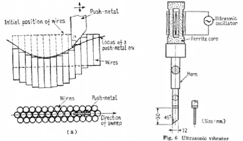
Some of the first academic research in the reconfigurable pin tooling field was conducted by the Nakajima group at the University of Tokyo [2]. Nakajima’s mold involved a matrix of tightly packed, smooth pins that were set to their intended height by an ultrasonically vibrating stylus, seen in Figure 6, sweeping across the grid’s surface with the correct profile. This method, like the tightly packed lead screws previously mentioned, has potential for a high resolution surface, as only a single pin setting actuator is needed and very small pins can be used. Potential problems with this method include the previously mentioned complexity of the multi-axis positioner and long reconfiguration time. In Nakajima’s 1969 article [8], he mentions that in his invention, as in all pin tooling machines, there is a practical limitation to the size of the pins used in any array. When the diameter of the pin decreases, so does the rigidity of the pins and subsequently the stiffness of the array. This is an important limitation to understand as reconfigurable pin tooling devices achieve greater resolution; array stiffness must be augmented by a method such as backfilling the spaces between pins with a fusible material [9] or perhaps incorporating a low grain size “jammable” material that can increase in stiffness by applying vacuum pressure [11].
Figure 6: Closely packed thin wires, set in place by sweeping, vibrating stylus; stylus vibrates ultrasonically to prevent adjacent pins from moving as well.
16
1.2.5
Reconfigurable mold stock
Multi-axis pin setting mechanisms (described in the previous two sections) have nearly the same level of complexity as conventional high speed machining of molds and dies, with the benefit of saving much wasted stock material generated in making single purpose molds or dies. A method of subtractive pin tooling developed by Zhijian Wang [9] incorporates both large interlocking threaded pins and conventional machining of those pins to quickly create molds for vacuum forming (Figure 7). First, large plastic pins are set to a coarse approximation of the desired mold with a method similar to the one described in Section 1.2.3. Next, a multi-axis milling machine creates the desired, smooth mold shape from the coarse approximation. Finally, this mold is then used for direct vacuum forming of plastics. This method is unique because instead of trying to directly create a mold from a grid of pins, the intent of the pin array is to conserve mold stock material and total machining time. If small changes are made to the design, the pins can be moved upwards slightly and the mold re-machined. This flexible rapid
prototyping technique saves both time and material cost, but still relies on expensive and complex machinery for both pin setting and machining.
Figure 7: Wang’s reconfigurable mold, before and after milling [9].
1.2.6
Interpolation and surface smoothing
Due to the discrete nature of all reconfigurable pin devices, an inter-pin interpolation method is commonly incorporated, usually sacrificing some resolution to provide a smooth,
non-dimpling forming surface [2]. Interpolation is typically accomplished by placing a flexible rubber layer on the hemispherical tops of pins and either drawing the rubber down by vacuum or relying on the force of molding to push it in place. Other methods of surface smoothing involve
17 the use of pivoting pin tips, shown in Figure 8, which rotate to the correct tangent position of the sheet of material being formed on them.
Figure 8: Pivoting pin heads used for surface smoothing [9].
1.3
Proposed design
Upon review of prior art and after performing a few simple tests of feasibility, a pin actuation scheme was generated, incorporating a moving magnetic plate and simple, digitally controlled, pin gripping clutches, shown below in Figure 9. To generate a contoured surface, the device would first release all micro-clutches and then move the magnetic plate to the top of its stroke, near the clutch array. Next, the magnetic plate, with all steel pins attached to it, would move downwards slowly. As the plate moves downwards, clutches are individually activated as their corresponding pins reach the correct height. When the magnetic plate reaches the bottom of its stroke, all the pins in the array will have been configured to form the desired topography. This design is advantageous as only one large actuation plate is required (versus the 3 axis pin setting required of other designs) and depending on the speed of the micro-clutches, the mold
reconfiguration cycle will be short.
18
1.4
Requirements
The pin actuation design proposed in the previous section can be constructed with simple steel rods with press-fitted or dip-coated plastic sheaths and a single-axis moving stage controlled by stepper motor. The challenge presented is the design and fabrication of an
electrically controlled micro-clutch that will fit in the area between the pins. Ideally, this design will be scalable to very small pin sizes and be able to withstand forming pressures—which become less and less per pin as the array becomes higher resolution.
1.4.1
Goals
Below are a few functional goals—elements of an ideal reconfigurable surface—that will aid design decisions as the project moves along.
Resolution: Pin array should be scalable to sub-millimeter pin size.
Size: Device should have no limit to possible surface area.
Resetting time: Array should take no longer than 20 minutes to completely reconfigure.
Forming pressure: Device should withstand forming pressures of 300 psi or greater. Although meeting all these goals is not necessary to create a useful forming device, keeping them in mind is important as the design progresses.
19
2
M
ICRO
-C
LUTCH
D
ESIGN
2.1
Requirements
As discussed in Chapter 1, the design of a digitally controlled micro-clutch is of vital
importance to the proposed actuation scheme (pictured in Figure 9). The functional requirements of this micro-clutch are as follows:
Limited space: Clutch can only take up an area equivalent to the area inside the outer diameter of the pin sheath and outside the diameter of the steel rod center (limited in x and y). However, there is little limitation to length of the clutch along the throw of the pin (unlimited in z-direction).
Electronic control: Due to the large number of clutching elements, electronic control is necessary to ensure accurate and repeatable clutching.
Clutching force: Each clutch should have the holding force necessary to allow the array to resist forming pressures of 300 psi or greater.
Actuation speed: Clutches must actuate fast enough to allow the array to reconfigure in less than 20 minutes.
2.2
Actuation Types
2.2.1
Thermal
Thermal actuation (via a chevron or asymmetric beam actuator) is an attractive method for pin clutching, as the forces involved in thermal expansion are more than enough to provide sufficient clutching force to meet the functional requirements. Negative aspects of thermal expansion include difficultly in control (possibly feedback is needed), and thermal gradients developing in the device (hot near the center, cold near the edges).
20
2.2.2
Piezoelectric
Piezoelectric crystals, using a similar method as the thermal actuator described above, would provide useful actuation without many of the thermally dependent negative effects outlined above—as the strain of piezo-actuators and thermal expansion are on the same order. However, manufacturing tiny piezo-actuators in a dense array is beyond the scope of the project with regards to funding and technical ability.
2.2.3
Shape memory alloy
Shape memory alloy was examined with great interest early in this project’s history, but the benefits of the high strain and small size were outweighed by the difficulty of manufacturing and low cycle-lifetime from sensitivity to over-straining.
2.2.4
Phase changing clutch (fusible alloy)
The use of a phase changing alloy retains some of the disadvantages seen in thermal actuators (thermal gradients and hot spots), but with promising capabilities for strong gripping force—potentially equal to the shear force of the alloy used.
2.3
Thermally actuating flexure
The first attempt to create a clutch that fit the needed requirements was based on a thermally buckling chevron beam clutching pins made of steel threaded rod —see schematic in Figure 10. The concept was that the crescent-moon shaped part of the beam would be threaded, and upon heating the beam to about 200 degrees C, the flexure would buckle enough to engage the threads of the pin, locking it in place. A rough approximation of the dimensions of the chevron beam were made from the equation shown in Figure 10, and finite element analysis was done on the beam to further optimize its length and width, keeping in mind the limitations of the fabrication process (in this case, micro-milling). Full dimensions of the array and the flexure are available in Appendix A. Flexure arrays were made from 6061 aluminum stock.
This design looked promising on paper, but proved very difficult to manufacture in practice. The final array design (pictured in Figure 11) was first partially cut out with an abrasive water-jet, and then the threads in the center of each flexure were tapped. Finally, the device was re-fixtured to a mill and the thin flexures were milled out. Placing electrical traces and resistive
21 heaters on the flexures—as was a suggested method of heating [7]—proved to be difficult. First, the aluminum flexure was anodized, to make it electrically insulated. Next, conductive paint was sprayed on over a laser-cut stencil to make a base for further electroplating. Copper was then electroplated on the conductive paint and high-resistance carbon paint was applied to the flexure to allow for direct heating of the flexures by resistive heating. Some success was seen in this method, but due the incredible complexity of creating only a few clutches, the concept was discarded as infeasible to make with conventional machinery, in the time constraints of this thesis project.
[
( )(
) ( )
]
( )
L = Unheated single beam length L’ = Heated single beam length a = Unheated bend angle
d = Displacement
Figure 10: Schematic of a chevron-type thermal actuator [10]; above equation was used to approximate the deflection needed; design was further refined in FEA.
22
Figure 11: Left: CAD design of flexure array, right: micro-machined array; this array is 4.25” square and features thermal fins along the perimeter to prevent the
device from uniformly heating and reducing the effects of thermal actuation.
2.4
Fusible alloy clutch
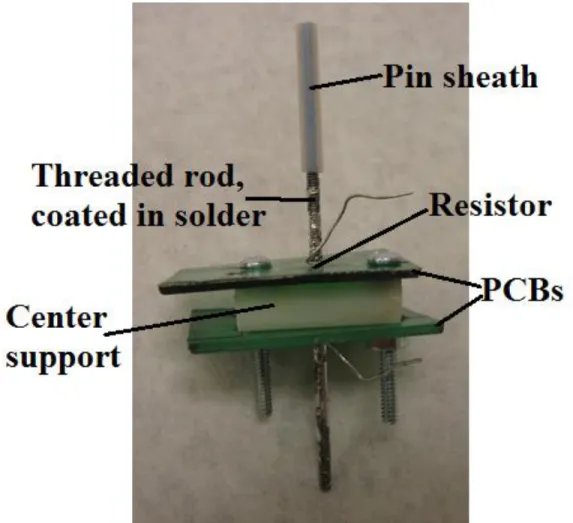
While working on the thermally actuating flexure concept described above, a lead screw from one of the pins I was working with became stuck in a drop of solder from another project. The idea struck me that one could use a solder type alloy coating on a threaded lead screw or notched rod to rigidly lock it in place when the alloy solidified. A bench test with a threaded rod, a hole laser-cut in Teflon and a soldering iron confirmed this idea. After experimenting with a few different resistive heating elements including nickel chromium wire and the steel rod itself, it was determined that using a conventional through-hole resistor as a heating element would be the easiest to obtain and attach to electronic components.
A single pin prototype was made, composed of two scrap PCB’s sandwiching a piece of laser-cut delrin, and a steel threaded rod dipped in Cerrolow 117, low melt solder, with a Teflon sheath (see Figure 12). A 900 Ohm resistor was inserted in parallel, near the threaded rod, electrically insulated from the low melt alloy by a neoprene spray coating. The prototype, although constructed in less than 30 minutes, worked admirably well, encouraging future work with this clutching concept. This clutching technique at this scale has a calculated holding force of around 20 pounds per pin (calculated from the estimated shear strength of the cylinder of solder surrounding the threaded rod, captured in the clutch array). This equates to over 1,000 psi per square inch of holding force in the 1/8” pin array. In reality, the pin can hold more than that
23 (as a 25 pound weight was hung from the pin successfully), but further tests need to be done to test exactly how much force is required to shear the pin out of its locked position. As for how the pin is being held in place by the solder, there are a few possibilities illustrated in Figure 13. The first theory is that the solder is able to wet to the copper plating around and inside the hole in the PCB, essentially soldering itself in place. The second and third theories are variations of a non-wetting scenario in which the PCB doesn’t adhere to the solder on the rod. Instead, the solder beads up enough around where the rod slides in the hole though the PCB, that when the solder hardens, a solid ledge of solder is formed, locking the pin in place. Further tests should be done with different types of holes (close fitting, loose, plated, non-plated) to determine the optimal condition for locking the threaded rod in place.
24 Fi gu re 13 : D iff er e nt p oss ibi li ti e s fo r so lde r a dh es ion of the thr ea ded rod to the PCB . O pti on 1 a ssu m es th a t the so lde r is a bl e to w et to th e pl a ti ng in t he P CB a nd pr ov id e a sol id conn ectio n. O pt ion s 2 a nd 3 a re v a ri a tio ns of a n on -w etti n g si tu a tio n w h er e the sol d er doe sn ’t a d he re to th e P CB , but be a d s u p e nou gh to lock t he rod i n p la ce w h en it th e sol d er coo ls.
25
2.5
Conclusions
Based on the available concepts and a few simple bench tests, it is clear that a proper
utilization of a fusible alloy clutch is the superior method for this thesis, as it has the potential to fulfill all the requirements listed at the beginning of this chapter and above all else, is very simple to manufacture. PCB’s can be professionally made for low cost, threaded steel rod is inexpensive to buy or make and a single axis linear actuator can be made for low cost as well. Potential problems with this concept include the low melt solder rubbing off the threaded rod and possible concerns about the use of heavy metals (the low melt solder used contains both lead and cadmium).
26
3
S
YSTEM
F
ABRICATION AND
I
NTEGRATION
3.1
System architecture
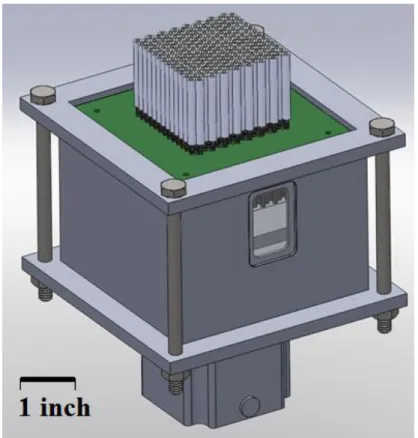
Keeping in mind the goals for the device, noted in Chapter 1 and the requirements of the clutch array to fulfill those goals, noted in Chapter 2, a complete device was designed, as seen below in Figure 14. Care was taken to make the device as simple as possible, while allowing easy swapping of the PCB and clutch array to experiment with different configurations and resolutions in the same device. Figure 14 is an image of the CAD model used to build the device and provide dimensions to design the PCBs.
27
3.2
Clutch array
3.2.1
PCB manufacture
To test how well the fusible alloy clutch system worked in an array, a low resolution PCB of 52 pins with 0.3” center to center spacing (hexagonally packed) was made by etching a single layer board by hand. Seen in Figure 15, this PCB featured through holes for the threaded pins, plated holes with traces for the resistors and other smaller holes spread evenly on the surface to allow for vacuum to be drawn around the pins. This vacuum pressure will be used to hold down the rubber interpolation layer and smooth the pins. Another use of these holes could be for forced air cooling of the array, helping to get rid of heat buildup over time.
While testing the low resolution array, a professionally made, high resolution PCB—Figure 16—was designed and ordered. This array has not one but six layers. Because of the layering, the number of pins could be quadrupled, and all the necessary electronics to control the array could be integrated directly onto the board, saving assembly time. A problem with this method is that it isn’t scalable in the x- and y- directions, as the number of layers in the PCB must
increase as the board gets larger. The number of layers must increase because the traces required to provide power to the resistors throughout the board have to be of a minimum width to provide sufficient current carrying capacity. Layering is needed to fit in all of these traces, adding to manufacturing cost and violating a goal of this project.
28
Figure 16: Manufactured, high resolution (0.15” pin spacing, 208 pins) PCB, design courtesy of Eric Marion [13].
3.2.2
Assembly challenges
An unforeseen challenge in assembling the low resolution PCB was simultaneously threading 52 resistor leads through 52 holes by hand. The feat was accomplished by tying thread onto each resistor wire after the array had been electrically insulated with a neoprene spray. These threads were then guided through their corresponding holes in the other PCB, shown in Figure 17, and the wires were coaxed through in this way. An easy solution to this problem would be to attach both resistor wires to the same PCB (leaving the resistor perpendicular to the board), instead of tackling the challenge of threading thousands of resistor wires simultaneously.
29
Figure 17: Resistor wires attached to black thread; thread was used to guide wires through their corresponding holes.
3.3
Pins
3.3.1
Structure
Pins were made from 2-56 threaded steel rods, with plastic rod threaded onto the end for a sheath (see Figure 18 below). The threads are important for the adhesion of the solder, and steel is an advantageous material due to its superior stiffness. Pin sheaths were made from Teflon for both its low friction and high melting temperature—making it an ideal choice in a
thermoforming device.
Figure 18: A low resolution pin, 0.3” diameter (top) and a higher resolution pin 0.15” diameter (bottom).
30
3.3.2
Surface wetting
It was noted that the steel rods that were obtained for the pins of the device offered poor surface wetting of the low melt solder (seem in Figure 19 below). Even wetting is important for the function of the solder clutch, as solder may rub off the rod if wetting is poor. To improve the wetting of the rod, all oils were removed from the surface with acetone before dipping in the low melt solder. Observing how well copper wets on PCBs, a clean threaded rod was electroplated with a thin layer of copper and then dip coated with low melt solder. The copper coating offered the best wetting of all—the solder was pulled deep into the threads and was quite difficult to rub off, even when pushed through a tight fitting hole. For the final device, a variety of different surface coatings should be tried, but copper plating looks like a good, inexpensive option.
Further tests were done on smooth steel rods and copper plated rods to compare the surface wetting characteristics to the threaded rods, as smooth rods are cheaper and easier to obtain than very small threaded rod. The smooth rod exhibited very poor wetting when compared to the threaded rod—this difference resulting from solder “wicking” into the threads of the rod.
Figure 19: Solder wetting of (top) oily threaded rod, (middle) clean rod, and (bottom) copper plated rod.
3.4
Magnetic plate
The initial design calls for a magnetic plate to attract the steel pins and pull them down. The strength of the magnet should be sufficient to pull each rod along, but not so strong that the rod won’t be able to be pulled off the magnet when the clutch is activated. Initially, I chose a single large square magnet, but upon installing it in the device, I found that the magnet produced a
31 rotation moment on many of the steel rods. The further away from the center of the magnet, the magnetic field lines were more curved—this effect puts a rotation force on the rods and makes them difficult to pull straight down. To remedy this, the single, large magnet was replaced by an array of smaller magnets with one installed at the base of each pin. This method worked
exceedingly well, as the magnets provided a centering effect on the rods if they became misaligned.
3.5
Vacuum seal and interpolation
In order to draw a vacuum through the device to pull down the interpolation layer, the whole structure needs to be air tight. Initially, this didn’t seem to be much of a problem, as the
structure was simple in geometry. However, even after installing gaskets, the device still would not hold a proper vacuum. By blowing air into the device, holes are more readily found (as a greater pressure difference is possible with positive pressure versus negative vacuum pressure) and sealed with gasketing or silicone sealant.
The interpolation layer was provided by a low durometer (10A Shore hardness) silicone rubber. This silicone is resistant to heat up to 600 degrees F, more than sufficient for use with many injection molded and vacuum formed materials. An added benefit of the reconfigurable geometry and the compliance of the silicone interpolation layer is that molds with a 90 degree relief angle are possible (in conventional molding, a sharp relief angle would prevent mold release.
32
4
F
UTURE
W
ORK
/
C
ONCLUSION
4.1
Introduction
Much work has been done in this thesis project to make the digitally reconfigurable surface a feasible and useful manufacturing tool for many applications. As the concepts studied in this project continue to evolve, continued brainstorming and revisiting each part of the device’s architecture is useful and will help to improve the device over time. In the below sections, a few improvements are discussed that may be incorporated into a later version of the device.
4.2
Improved scalability
In Section 3.2.1 a limitation of the device is discussed where the PCBs require more layers as the array becomes larger in the x- and y- dimensions. A reconfiguration of the electronics, pictured in Figure 20 below, is possible to allow for unlimited transverse scalability. The
improvement lies on using the pins themselves as the electrical transmission lines through which their corresponding resistor heater receives power. Controlling electronics can be placed in the plentiful space below the z-movement stage and provide power through the pins via the pin’s contact with a gold-plated conductive magnet. With this arrangement, the PCBs in the clutch area need only to be a single layer, as the upper PCB can transfer power to the resistor from the connection made by the solder on the electrified steel rod to the metal plated hole around it. By making the entire lower PCB a ground common, this completes the circuit.
33
Figure 20: Rearrangement of controls electronics for improved scalability.
4.3
Conclusion
After working on this project for nearly a year, I am personally very enthusiastic about the progress made so far and predict a fully functional, scalable vacuum forming mold will be finished by the end of this year. I will be continuing this work in my Master’s thesis research in the Mediated Matter group at the MIT Media Lab and look forward to making further
improvements on the machine, improving its scalability and reducing the pin size to a point where injection molding could be done with this reconfigurable mold concept.
34
R
EFERENCES
[1] Papazian, J. M. (2002). Tools of Change: Reconfigurable Forming Dies Raise the Efficiency of Small-Lot Production. Mechanical Engineering, 52-55.
[2] Munro, C., & Walczyk, D. (June, 2007). Reconfigurable Pin-Type Tooling: A Survey of Prior Art and Reduction to Practice. Journal of Manufacturing Science and
Engineering, 551-565.
[3] Conversation with David Hardt, M.I.T, 5-18-11
[4] Walczyk, D. F., & Hardt, D. E. (1998). Design and Analysis of Reconfigurable Discrete Dies for Sheet Metal Forming. Journal of Manufacturing Systems, 436-454.
[5] R.E. Robinson, "Design of an Automated Variable Configuration Die and Press for Sheet Metal Forming," MS thesis (Cambridge, MA: Dept. of Mechanical Eng., Massachusetts Institute of Technology, 1987)
[6] K.B. Ousterhout, "Design and Control of a Flexible Process for Three-Dimensional Sheet Metal Forming, PhD thesis (Cambridge, MA: Dept. of Mechanical Eng. Massachusetts Institute of Technology, 1991).
[7] Berteau, J. (1994). Patent No. 5,330,343. CA.
[8] Nakajima, N. (1969). A Newly Developed Technique to Fabricate Complicated Dies and Electrodes with Wires. The Japan Society of Mechanical Engineers, 1546-1554. [9] Wang, Z. (2009, August). Rapid Manufacturing of Vacuum Forming Components
Utilising Reconfigurable Screw-Pin Tooling. PhD Thesis. University of Nottingham. [10] Sinclair, M. (2000). A High Force Low Area MEMS Thermal Actuator. 7th Intersociety
Conf. on Thermal and Thermomechanical Phenomena in Electronic Systems, (pp.
127-132). Las Vegas, NV.
[11] Conversation with Steven Keating, Mediated Matter M.S. candidate, 5-9-11 [12] Conversations with Robert Panas, PCSL, MIT. Spring, 2011
[13] Marion, E. “Digitally Reconfigurable Surface, A” 6.UAP Final Project (Cambridge, MA; Dept. of Electrical Eng. and Computer Science, 2011)
35
A
PPENDIX
A
36 Dimensions and spacing of a grid of chevron flexures (in inches)


![Figure 3: A modular array of eight motors, encoders and lead screws used in the device pictured in Figure 2 [2].](https://thumb-eu.123doks.com/thumbv2/123doknet/14679336.558833/12.918.347.602.315.994/figure-modular-motors-encoders-screws-device-pictured-figure.webp)
![Figure 5: Interlocking pin array actuation; accomplished by a three axis robot able to turn screws to desired heights [7]](https://thumb-eu.123doks.com/thumbv2/123doknet/14679336.558833/14.918.288.629.447.890/figure-interlocking-array-actuation-accomplished-screws-desired-heights.webp)
![Figure 7: Wang’s reconfigurable mold, before and after milling [9].](https://thumb-eu.123doks.com/thumbv2/123doknet/14679336.558833/16.918.171.753.585.792/figure-wang-s-reconfigurable-mold-milling.webp)