A Combined Microfluidic/Dielectrophoretic
Microorganism Concentrator
by
Nitzan Gadish
Bachelor of Science, Electrical Science and Engineering
Submitted to the Department of Electrical Engineering and Computer Science in Partial Fulfillment of the Requirements for the Degree of
Master of Engineering in Electrical Engineering and Computer Science
at the
Massachusetts Institute of Technology
August 15, 2005
C 2005 Massachusetts Institute of Technology. All rights reserved.
The author hereby grants to M.I.T. permission to reproduce and
distribute publicly paper and electronic copies of this thesis MASSACHUSETTS INSTnlfTE
and to grant others the right to do so. OF TECHNOLOGY
AUG
14
2006
LIBRARIES
Author: ____ _______________
D
bartment
of Electrical Engineering and Computer Science August 15, 2005 Certified by: Joel Voldman Thesis Supervisor Accepted by: _ Arthur C. Smith Chairman, Department Committee on Graduate Theses 1A Combined Microfluidic/Dielectrophoretic
Microorganism Concentrator
By
Nitzan Gadish
Submitted to the
Department of Electrical Engineering and Computer Science August 15, 2005
in Partial Fulfillment of the Requirements for the Degree of Master of Engineering in Electrical Engineering and Computer Science
ABSTRACT
This thesis presents the development of a high-throughput microfluidic microorganism concentrator for pathogen detection applications. Interdigitated electrodes lining the bottom of the channel use positive dielectrophoretic forces to trap particles. A passive mixer is used to circulate the liquid in the channel, transporting particles to within the trapping region of the electrodes. Samples are extracted and their concentrations measured using a spectrophotometer. Concentration enhancements up to 40x at 500 pl/min flowrate using polystyrene microspheres and up to lOx at 100 pl/min flowrate using B. subtilis spores are achieved.
Thesis Supervisor: Joel Voldman
ACKNOWLEDGEMENTS
I would like to acknowledge the many people without whom this project and I would not have evolved to the state we are in. I am grateful for the advice, guidance, and support I have been fortunate enough to receive.
First and foremost, I would like to thank my advisor, Joel Voldman, for his guidance and assistance in bringing this project from idea to working device. I would also like to thank Joel for putting together such a friendly, supportive, smart group of people that I had the privilege to work with!
I owe special thanks to Mike Vahey, for always having the time and knowledge and patience to help answer any question, technical or otherwise; and to Luke Theogarajan
for one idea in particular, and many others in general.
Additional huge thank yous to the members of the Voldman group (as I knew it) - Adam Rosenthal, Brian Taff, Lily Kim, Salil Desai, Katya Puchala - for help from modeling to machining to experiments and everything in between. I wish you endless success and happiness and above all, some time off! Thanks also to Rikky Muller for introducing me to this field in the first place.
I would like to thank the MTL staff, especially Dave Terry and Paul Tierney, for teaching me the ways of the clean room. For project funding, thanks to Charles Stark Draper Laboratory and Siebel Systems.
I also owe many thanks for support of a non-technical nature. I would of course like to thank my family for their everlasting confidence in me. A huge thanks also to Mariana Markova for always understanding. And last but certainly not least, the biggest thank you of all to Chris... for everything.
TABLE OF CONTENTS
CH A PTER 1: IN TR O DU CTION ... 8
L IBACKGROUND ... 8
1.2 DEVICE OVERVIEW ... 10
1.3 THESIS OVERVIEW ... 12
CHAPTER 2: DESIGN AND MODELING ... 13
2.1 DIELECTROPHORESIS ... 13 2.2 SPORES ... 16 2.3 ELECTRIC FIELDS ... 18 2.4 M IXER ... 23 CHAPTER 3: MICROFABRICATION ... 26 3.1 M ASKS ... 26 3. L .1 Electrode M ask ... 26 3.1.2 SU-8 M asks ... 28 3.2 M ICROFABRICATION PROCESS ... 30 3.2.1 Gold Processing ... 30 3.2.2 SU-8 Processing ... 32 3.3 PACKAGING ... 35 3.3.1 Components ... 35 3.3.2 Assem bly ... 36
CHAPTER 4: MATERIALS AND METHODS ... 39
4.1 M ATERIALS ... 39
4. L I Spores ... 39
4.1.2 Test Particles ... 41
4.1.3 Sylgard Prime Coat ... 43
4.2 M EASUREMENT TOOLS ... 46 4.2.1 M icroscope ... 46 4.2.2 Spectrophotometer ... 47 4.3 TEST SETUP ... 48 4.4 EXPERIMENT ... 48 CH APTER 5: R ESULTS ... 52 5.1 D EVICE CHARACTERIZATION ... 52 5. L I Trapping Characteristics ... 52 5.1.2 M ixer ... 54 5.2 CONCENTRATION ENHANCEMENT ... 56
CHAPTER 6: CHALLENGES AND FUTURE WORK ... 59
6.1 M ODELING ... 59
6. 1.1 pDEP ... 59
6.1.3 Experim ents ... 61
6.2 SPORES... 62
6.2.1 M odeling ... 62
6.2.2 Staining ... 63
6.3 A CHIEVING A CONCENTRATION ENHANCEMENT ... 64
6.3.1 W ith beads... 64
6.3.2 W ith spores... ... 65
6.3.3 Trapping Efficiency... 65
CH A PTER 7: CO N CLU SIO N ... 67
7.1 CONTRIBUTIONS... 68
APPENDIX: FABRICATION PROCESS FLOW ... 69
LIST OF FIGURES
Figure 1-1: D evice overview ... 11
Figure 2-1: D ielectrophoresis ... 14
Figure 2-2: Microscope image of B. subtilis spores ... 17
Figure 2-3: Electric field stream lines... 18
Figure 2-4: Electric-field reach simulation... 20
Figure 2-5: Picking an optimal electrode width... 21
Figure 2-6: Electric field strength simulation ... 22
Figure 2-7: M ixer dim ensions... 24
Figure 3-1: Electrode m ask... 27
Figure 3-2: SU -8 m ask ... 29
Figure 3-3: Electrode fabrication process... 31
Figure 3-4: Photograph of a microfabricated Pyrex die... 32
Figure 3-5: Channel fabrication process ... 34
Figure 3-6: Illustration of a packaged device ... 35
Figure 4-1: Comparison of three spore stains ... 40
Figure 4-2: Predicted Re[CM] for magnetite-coated polystyrene microspheres... 42
Figure 4-3: Improving the release... 44
Figure 4-4: Determining the effect of Alconox on spores ... 45
Figure 4-5: Calibration of NanoDrop measurements... 47
Figure 4-6: Experiment setup... 48
Figure 4-7: Effect of Alconox on NanoDrop measurement... 50
Figure 4-8: Output data from a typical experiment ... 51
Figure 5-1: Device characterization... 53
Figure 5-2: Characterization of mixer effect on device performance... 54
Figure 5-3: Microscope photograph of channel showing effect of mixer on trapping ... 55
Figure 5-4: Three plots showing concentration enhancement with beads... 56
Figure 5-5: Concentration enhancement using spores ... 57
Figure 6-1: Plot of z-directed dielectrophoretic force... 60
Figure 6-2: Visual indication of spore staining... 64
LIST OF TABLES
Table 1: Channel dimensions based on mixer publications... 25Chapter 1: Introduction
This thesis presents the development of a microfabricated electric-field device for microorganism concentration to aid in the detection of biological warfare agents. The intended objective of this concentrator is to preconcentrate a sample of bacterial endospores in deionized water for downstream detection.
1.1 Background
Pathogen sensing is essential in many applications, including medical systems, water purification, and biological warfare agent detection. Among the approaches that exist for pathogen detection, microfluidic devices are especially appropriate as they operate optimally with particles on the micron scale. One such microfluidic pathogen detector is the pFAIMS, introduced by R. A. Miller et al. [1]. A limitation of this and other microfluidic pathogen detectors is the dependence of their sensitivity and detection threshold on the concentration of the sample they process. A concentrated sample of a given particle makes that particle easier to detect.
Another limitation, which is generally common in microfluidics, is the mismatch between the volume of samples obtained by standard collection methods and the volume a microfluidic device can process in a reasonable amount of time. Collected sample volumes are often on the order of milliliters, whereas microfluidic devices process volumes on the order of microliters. This mismatch should be corrected not by discarding the majority of the sample but by discarding the majority of the liquid while keeping all
of the particles of interest.
A concentrator can be used to overcome both the sample preparation and the volume mismatch limitations by accumulating the particles of interest from a sample and resuspending them in a smaller volume of solution. The result is a highly concentrated sample of a volume that can easily be processed by a pathogen detector or other microfluidic device.
Concentration requires selectively applying a force to the particles of interest, but not to the liquid in which they are suspended. Common methods of concentration include membrane filtering and centrifugation.
Centrifugation accelerates particle settling in a liquid medium by applying a centrifugal force that acts on the difference between the particle and the medium densities. Centrifugation is fast, processing volumes on the order of 10 ml in a few minutes. It is often performed using a bench-top centrifuge, however, and requires human intervention steps (pipetting, aspirating, loading samples). In general, it does not readily lend itself to miniturization and is impractical for integration with microfluidics.
Membrane filtering utilizes a porous membrane to selectively trap particles larger than the pores while the medium flows by unaffected. Membrane filtering is efficient in trapping particles above a certain size. However, as particles accumulate on the membrane, they obstruct the flow path of the medium; membranes are therefore prone to clogging. Additionally, it is difficult to remove a sample from the membrane. Analysis must be performed at the membrane, so in this case the concentration method shapes the design of the rest of the system, as in [2]. Following analysis, a backflow has to be generated to remove particles from the membrane, requiring a more complicated flow setup. Finally, once a membrane filter has been installed in a fluidic system, it cannot easily be disabled or removed.
Both centrifugation and membrane filtering are generally macro-scale techniques. It is desirable, however, to achieve concentration on the micro-scale. A micro-scale concentrator could be integrated with a microfabricated detection element, creating a complete microfabricated system. Direct integration of the two components eliminates the need for human intervention in delivering the concentrated sample to the detector.
Several methods exist for concentrating particles at the microscale. Several acoustic microconcentrators have been developed [3-5] that concentrate particles by focusing them to the nodes or antinodes of standing acoustic waves. Membrane filtering has also been performed on the microscale [2].
An alternative approach to concentrating particles on the microscale is to use electric fields to either apply forces to a charged particle (termed electrophoresis), or to
induce a dipole in a particle and act on the dipole. The latter method is known as dielectrophoresis (DEP).
DEP refers to the force on polarizable particles in a spatially non-uniform electric field, and provides a suitable method for manipulating microparticles in liquid suspension. It applies forces on the rnicroscale and therefore works optimally with micro-scale particles and devices, integrating seamlessly with microfluidics. Two types of forces can be exerted: particles can be pulled toward points of maximum electric field (termed positive DEP, or pDEP) or pushed toward locations of minimum electric field (termed negative DEP, or nDEP). Dielectrophoretic forces can be produced using simple planar electrodes, making devices simple to fabricate. Moreover, electric fields can be quantitatively modeled, enabling optimization of device design. Finally, DEP is an active mechanism that can easily be turned on and off.
Several DEP concentrators have been presented in the literature. Particle accumulation has been demonstrated using both pDEP [6-8] and nDEP [9]. However, sample concentration is often evaluated optically on-chip. Furthermore, devices are often operated at low (-1 pl/min) flowrates and tested using large (-5-ptm-diameter) particles.
The concentrator presented here is designed to prepare a sample for pathogen detection; specifically, it is designed to interface between an air sampler, which suspends particles from air into a known liquid, and a pathogen detector. The concentrator is therefore targeted to concentrate B. subtilis endospores (-1 ptm diameter) suspended in deionized water at 500 /min throughput. It is implemented as a microfluidic device so that it is integrable into a microfluidic system. Concentrator performance is assessed quantitatively, by extracting a sample and directly measuring its concentration.
1.2 Device Overview
The initial device design consists mainly of a simple microfluidic channel, with electrodes lining the bottom and grooves lining the top (Figure 1-la). The concentrator utilizes pDEP, pulling particles to points of maximum electric field, to collect particles. A passive mixer circulates the liquid in the channel, bringing particles to within the trapping region of the electrodes, as illustrated in Figure 1-lb. As a sample of low particle
concentration flows through the channel, the electrodes selectively apply a downward force to the particles. The surrounding medium is not affected and is sent to waste. When enough particles have been accumulated on the electrodes, the force is deactivated and the particles are resuspended into a smaller volume, thereby producing a concentrated
sample (Figure 1-1c).
Interdigitated electrodes are used to apply a pDEP force to collect particles. This force is limited by the applied electric field and decreases exponentially with distance from the electrodes. Moreover, for a given voltage, the field exhibits a characteristic tradeoff between its strength at the bottom of the channel and its reach into the channel. The device must be designed such that the DEP force is strong enough to both trap and hold particles in high flowrates.
(A)CHAOTIC
MIXER INTERDIGITATED E LECTRODES
CHANNEL
mxrchaotic flow aIwe
__1+~lminar flow~'
+---- tric field 4W i
couection Relexse
Figure 1-1: Device overview
(A) Illustration of the main concentrator components, showing an enclosed microfluidic channel. Grooves in the top of the channel create a passive mixer that circulates the fluid and particles as illustrated in (B). Interdigitated electrodes lining the bottom of the channel trap and accumulate particles, as illustrated in (C). Accumulated particles are released into a concentrated suspension.
1.3 Thesis Overview
In this thesis, I present the development of the microorganism concentrator. I begin with an overview of dielectrophoresis and a description of the modeling and its outcomes in Chapter 2. I then outline the fabrication and packaging processes in Chapter 3. In Chapter 4 I describe the materials and methods I employed when performing experiments. In Chapter 5, I present the results I obtained, followed by challenges I encountered and possible improvements in Chapter 6. I conclude the thesis in Chapter 7.
Chapter 2: Design and modeling
Developing a system that produces a concentration enhancement at sufficiently high throughput requires a quantitative characterization of the system. Fortunately, the expertise of our research group lies in modeling systems that combine dielectrophoresis with simple microfluidics. We have developed modeling software [10] that calculates the trajectory of a particle subjected to electric fields and flow. Systems designed in our lab [9-13] show that the predictions made by this tool are close to experimental results.
This concentrator consists of two main components: the electrodes, which trap particles, and the mixer, which circulates the liquid to bring particles to within reach of the electrodes. To fully characterize the device, it is necessary to model both of these components, as well as the particle suspension to be concentrated. I modeled the system to predict its behavior and to determine optimal dimensions and operating parameters. In this chapter I describe the modeling process and how I used the results to design the concentrator.
2.1 Dielectrophoresis
The concentrator utilizes the properties of dielectrophoresis (DEP) to trap and concentrate B. subtilis spores. Dielectrophoresis refers to the force exerted on a polarizable particle by a spatially varying electric field. By acting on differences between the electrical properties of the particle and those of its surrounding medium, the electric field polarizes the particle and then acts on the induced polarization. If the particle is small compared to the length scale typical of the field nonuniformity, the induced polarization can be approximated as a dipole similar to that induced by a uniform electric field. The spatially varying field exerts a force of different magnitude on either side of this dipole, resulting in a nonzero net force and therefore in particle motion.
Based on differences in electrical properties between the particle and the medium, the particle will exhibit either negative dielectrophoresis (nDEP), in which it is pushed toward electric-field minima, or pDEP, in which it is pulled toward electric-field maxima.
If the particle is more polarizable than the surrounding medium, the path of least resistance for the electric field is through the particle. Negative charges will aggregate at the end facing the positive electrode directing the electric field into the particle; positive charges aggregate at the end of the particle facing the negative electrode, directing the electric field back out of the particle. The result is a dipole oriented opposite the electric field, as illustrated in Figure 2-la. Opposite charges attract and the particle is pulled toward the point of maximum electric field, thus undergoing pDEP.
\ Net Forc i/ -V I/ +V - Net +++ Net orc Fr Vv Figure 2-1: Dielectrophoresis
(A) Positive dielectrophoresis. A dipole is induced opposite the direction of the electric field, and is attracted toward the point of maximum electric field. (B) Negative dielectrophoresis. The dipole is oriented in the same direction as the electric field, electric field minima.
Shigh-particle lOW-particle + induced -dipole * electric field J electrodes and is repelled toward
The opposite is the case if the particle is less polarizable than the medium. In this case, positive charges aggregate at the end of the particle nearest to the positive electrode, diverting the electric field out of the particle and toward the more polarizable medium. The dipole is oriented in the direction of the electric field, as illustrated in Figure 2-lb, and gets repelled away from the point of maximum electric field, thus undergoing nDEP.
F +V
The polarizability of the particle is a lumped measure of its electrical conductivity and permittivity. For a uniform particle, the polarizability is defined as
mp = 8m,p + ' (2-1)
where e is permittivity, o- is electrical conductivity,
j
is -1, and co is the frequency of the applied electric field. Subscripts m and p indicate properties of the medium and particle, respectively. This equation shows that polarizability is dominated by conductivity at sufficiently low, and permittivity at sufficiently high operating frequencies.For systems in which higher orders of polarization (e.g. quadrupoles, octopoles) can be neglected, the dielectrophoretic force is derived by calculating the force exerted by a spatially varying electric field on a dipole induced by a uniform field [14]. For a homogeneous spherical particle of radius R, the dipole moment is induced by a uniform
electric field Eo(r) is
p = 41rEMR' E(_r)r !-p r (2-2)
Based on the assumption of negligible higher-order polarization, this moment is approximately equal to that induced by a spatially varying electric field E(r) that is
similar to Eo(r) near the particle. The force exerted on a dipole by an electric field t is
defined as f = p -yV. Applying this to the dipole moment above yields the DEP force:
- 2
E(r) is the complex applied electric field and co is the frequency of the field.
CM(co) is the complex Clausius-Mosotti (CM) factor, defined as:
CM 4 ! & (2-4)
The CM factor is a lumped measure of the polarizabilities of the particle and the medium relative to each other. For a homogeneous spherical particle, the real part of the CM factor can vary between -0.5 and 1. The sign of the CM factor dictates the polarity of the dielectrophoretic force. If the CM factor is negative, the particle will undergo nDEP and will be pushed toward electric-field minima; if the CM factor is positive, the particle will undergo pDEP and will be pulled toward electric-field maxima. Moreover, the magnitude of the DEP force is proportional to the magnitude of the CM factor. These observations imply that, for exactly similar field gradients, a stronger force can be produced by pDEP than nDEP, motivating the use of pDEP in the device.
In this device, both the medium conductivity and the operating frequency are design parameters. To achieve a pDEP force of high magnitude, I chose deionized water as the medium because of its low conductivity. I also chose to operate the device at low (~500 kHz - 1 MHz) frequencies so that conductivity dominates in the region of operation. Bacterial spores have higher conductivity than deionized water, so these choices enable the use of pDEP to accumulate, and thereby concentrate, the spores.
2.2
Spores
The target organism for concentration in this device are endospores of the bacteria
Bacillus subtilis (B. subtilis). An endospore is a resting stage in the life cycle of some
bacteria that enables a bacterial colony to survive harsh conditions [15]. Spores are therefore resistant to a variety of environmental stresses such as lack of nutrients, chemical disinfectants, and even radiation. B. subtilis spores are non-pathogenic and are often used as a safe substitute for B. anthracis, commonly known as Anthrax. Anthrax is
used as a biological warfare agent, and is distributed in spore form due to its resistant nature as such.
Figure 2-2: Microscope image of B. subtilis spores
Taken using a 63x objective on the microscope described in Section 0. Using image processing techniques, I have estimated the average spore radius to be approximately 500 nm.
Most of the information that exists about Bacillus endospores describes their composition and size [16, 17], as well as methods for killing them, e.g. [18-20]. To my knowledge, no published information exists about their dielectric properties. I have used microscope photographs of the spores, such as the one shown in Figure 2-2, to estimate their size at about 1 pm in diameter, which agrees well with published values. However, without information on their dielectric properties, it is impossible to calculate a CM
factor for the spores and thus predict their behavior when subjected to electric fields. To overcome this limitation, I have modeled the spore as a homogeneous spherical particle 1 pm in diameter and assumed a CM factor of 0.3 for all simulations. Section 2.1 showed that the CM factor for positive dielectrophoresis has a maximum value of 1. A CM factor of 0.3 is therefore a reasonably conservative estimate.
2.3 Electric Fields
The electric fields in this concentrator are produced by a set of interdigitated electrodes lining the bottom of a microfluidic channel. Interdigitated electrodes produce a wide region dense with electric field maxima at which particles can be trapped, resulting
in near-uniform trapping along the length of the channel. Due to their periodicity and symmetry, interdigitated electrodes are relatively simple to microfabricate and to analyze. A closed-form analytic solution exists for the electric field produced by interdigitated electrodes, published
by Chang et al. in [21]. Streamlines Electric Field Streamlines 200
of the electric field produced by this C
solution are shown in Figure 2-3. I 150 coupled this solution with our
modeling software to predict the W 100 dielectrophoretic force on a particle ..
50 of known CM factor or dielectric 8
properties. 0 50 100 150 200
Our modeling software, Position Along Channel Length, x (stm) ForceSim, is a suite of Matlab Figure 2-3: Electricfield streamlines
software that was developed by our Electric field streamlines (plotted in blue) research group [10]. This software produced by interdigitated electrodes (illustrated calculates the trajectory of a particle in red and black) of 20 pm width and spacing. suspended in a medium, as determined by the flow rate of the medium and by an electric field. The suite takes as its inputs the system parameters: an electric-field geometry, dielectric properties of the particle and its surrounding medium, and channel dimensions, among others. It uses these inputs to compute the drag, dielectrophoretic, gravitational, and lift forces exerted on the particle. For a particle to be trapped, the dielectrophoretic force on the particle has to be stronger than the drag force imposed by the flow. The program balances these forces, and uses the resulting net force to compute and draw the trajectory of a particle as it flows through the channel, and thus determine whether a set of operating conditions enables the electric field to trap the particle.
I used this tool to predict the trajectory of a spore in a channel, while varying parameters such as flow rate, electrode width and spacing, particle start height, and CM factor. Based on these simulations, I have come up with relationships that have enabled me to design the concentrator.
Interdigitated electrodes exhibit a tradeoff between the strength of the electric field and how far it reaches above the surface of the electrodes. For a given applied voltage, this tradeoff is controlled by the dimensions of the electrodes ([electrode width] = [spacing between electrodes] = d). Narrow electrodes spaced close to each other result in stronger, more localized electric fields. Wider electrodes spaced farther apart increase the reach of the field but decrease its strength.
In the context of this concentrator, the reach of the electric field controls how well the device can trap particles from within the channel. The strength controls the ability to hold particles against flow once they have been trapped. To determine the optimal electrode dimensions, I found it useful to decouple the reach and strength from each other and investigate each separately. I used simulations of the electric field reach to define the electrode dimensions, and simulations of the strength to set the operating conditions, as described in the next few paragraphs.
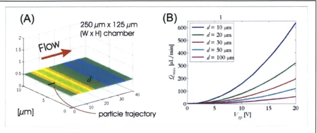
The reach of the electric field controls the height from which particles can be trapped, as well as the distance they travel in flow before they are trapped. Every set of operating conditions has a maximum flowrate associated with it beyond which the electric field is unable to hold particles against flow. Reach can be considered separately from strength if the flow is slower than the maximum flowrate associated with the simulation operating point. I investigated electric-field reach by starting a particle at varying heights h above the channel bottom and measuring the resulting capture distance. I have defined the capture distance to be the distance in the direction of flow that a particle travels before it is trapped (see Figure 2-4a). One instance of an electric-field reach simulation is shown in Figure 2-4a. The particle starts at 15 pm above the channel bottom and is gradually pulled toward the bottom by the electric field.
(A)
2(B)
35 0 25 ym x. 125 pim S(W x H) chamber _'_300-10 Particle 8 5 i 5,h t~lecory .3200 150 10 o 100 1000 0500 10 20 30 40Figure 2-4: Electric-field reach simulation.
(A) ForceSim simulation output showing a particle with starting height h = 15 pm being
trapped by 10-pm-wide electrodes, resulting in a capture distance of 100 gm. (B) Plot of capture distance vs. electrode width for 15 pm start height, with same conditions as in (A). For h = 15 pm, the electrode width that minimizes capture distance is approximately 15 gm.
In the results of the reach simulations, I observed that for every height at which the particle starts, there exists an electrode width d that minimizes the capture distance (Figure 2-4b). This result is independent of voltage, flowrate, and CM factor. Varying these parameters changes the value of the capture distance, but the electrode width that minimizes the capture distance remains the same. The relationship between electrode width and start height is a one-to-one linear relationship and is shown in Figure 2-5.
I used this relationship, in combination with an expected particle starting height, to determine the characteristic electrode dimension d. I chose the starting height based on the flow profile in the Staggered Herringbone Mixer, discussed further in Section 0. Published mixer results confirm mixing only in the central 50% of the channel cross-section [22]. This implies that the lower 15% of the 100-pm-deep channel is less well-mixed than the central region. Within these 15 pm, the mixer no longer circulates particles as efficiently, so this is where trapping needs to be optimized.
(A)
(B)
1000: 20 5 Q=25 d/min 1-h = 10 m5 = 12.5 p/min S100. -h = 15 pm X -~ *...* d=h 10& 10~ 10 2 10 50 0 5 10 15 20d (pm) dthat minimizes capture distance [pm]
Figure 2-5: Picking an optimal electrode width.
(a) Plot of capture distance vs. electrode width for particles starting at 5, 10, and 15 jim above the channel bottom. For every start height, there is a corresponding electrode width that minimizes capture distance. (b) There is a linear relationship between start height h and the corresponding electrode width that minimizes capture distance. This relationship is independent of flowrate, voltage, and CM factor, though varying these parameters does change the capture distance.
Ideally, to optimize trapping within 15 pm, the start height should be 7.5 pim. However, based on the relationship in Figure 2-5b, this would require about 6-jim-wide electrodes, which pushes the processing capabilities available to me. For a geometry that is relatively simple to fabricate, I chose 10 jim as the nominal electrode width and spacing. 10 jim is still relatively narrow, increasing the electrodes' vulnerability to shorting. I therefore fabricated two wider sizes as well. First, I chose a 50-pm width, which targets a start height that is half the channel depth and is therefore optimal for a channel without a mixer. Second, I chose a 25-pm width as it combines the ease of fabrication of wide electrodes with the electric field strength of narrow electrodes.
Once a particle is trapped, the strength of the electric field determines the ability to hold it against flow. I quantified strength using the maximum flow rate against which the electric field can hold a spore. To decouple the strength from the reach of the electric field, I simulated particles starting on the channel bottom (h = 0). This demonstrates how a particle behaves after it has been trapped, and eliminates the need to simulate the
trapping, which shortens the length (in the direction of flow) that needs to be simulated: due to the periodicity of the electric field, all electrodes exhibit equal strength and I needed to simulate only one electrode. Figure 2-6a shows an output of a simulation in which the particle is held by the electric fields. The trajectory of the center of the particle is plotted. The particle starts and remains at the bottom of the channel (center 0.5 pm, which is the particle radius, above channel bottom) and travels (in the direction of flow) only until it reaches the point of maximum electric field.
250 pm x 125 pm (W x H) chamber 0 5J 1 20 pm] I particle trajectory
(B)
600 -400 100i -d= to in -d= 20 jim d= 30irn d= 50iui - d tO ii "0 5 10v
* M Figure 2-6: Electric field strength simulation(a) Output of a ForceSim simulation showing the streamline of a particle held by an electric field. (b) Electric-field strength simulations yield this design curve and the relationships in Equation 4.
I used the strength simulations to establish relationships the dependence of the maximum flowrate on several system parameters (see Figure 2-6b):
Q.
0C
YQ.
oc V2Q.
occRe{CM}.(2-5)
Q
m is the maximum flowrate against which a particle can be held; d is theelectrode width, also equal to the spacing between electrodes; V, is the peak voltage
(A)
difference between the electrodes; and Re[CMi is the real part of the particle CM factor. Of these four parameters, only d is set in the device design. The remaining three, while coupled together, do not need to be set in the device design. These parameters can be adjusted during testing to tune the performance of the device to account for the unknown spore properties and meet the design specification.
For example, if the actual CM factor of the spores is 0.3, which is the value I used in simulation, then the modeling predicts that 18 Vpp are required to hold the spores against a flowrate of 500ptl/min. If the CM factor of spores is lower than 0.3, the applied voltage can be increased to compensate. If the CM factor is higher than the value used in the simulations, the voltage can be lowered, or a high voltage can still be used to achieve an increased throughput. Thus, the device is robust to a range of CM factors and the dielectric properties of the spores do not need to be extracted. Moreover, for a conservative estimate of the CM factor, simulations predict that the device meets the design specification.
2.4 Mixer
The passive mixer used in this concentrator is the Staggered Herringbone mixer, introduced by A. Stroock et al. in [22]. The mixer consists of grooves in the channel top or bottom that are oriented diagonally with respect to the direction of flow (Figure 2-7b). The grooves create helical flows in opposing directions (Figure 2-7a), and the mixer mixes by alternating the direction of the helix every half-cycle (Figure 2-7c).
The resulting fluid behavior is chaotic and is therefore difficult to model and integrate with the electric field models. However, while the flow profile throughout the channel is different in a simple rectangular channel than in a channel with the mixer, the average fluid velocity close to the channel walls is similar. Because spores are trapped by electrodes on the channel bottom, it is reasonable to use a rectangular channel to predict the strength of the electrodes and thus the maximum flow rate against which they can hold a particle.
112
h
yh 1
\2n/q \0 cycles: x Z % cycle: cycle: 100 pimFigure 2-7: Mixer dimensions.
(A) Illustration of a cross-section of the flow profile in consecutive half-cycles of the mixer. (B) Illustration of the Staggered Herringbone Mixer. Also Defines the dimensions used in Table 1. Note that h defines the average channel height (channel depth plus half the mixer grooves), and ah defines half the mixer groove depth. In this illustration (borrowed from [22]) the mixer is located on the bottom of the channel, whereas in the concentrator it is located on the top. (C) Confocal cross-section micrographs of a mixing channel, showing a cycle of fluid mixing. Fluidic input configuration is shown by the orange bands in (B).
Results published in [22, 23] define relative channel dimensions that produce optimal mixing. The channel and mixer are fabricated using a two-layer SU-8 process, where the first layer defines the channel and the second defines the mixer. To simplify the fabrication process, I chose a channel depth of 100 pm, as uniformity becomes difficult to control beyond this thickness. The remaining channel dimensions are defined by relationships in the publications ([22, 23]). The dimensions are illustrated in Figure 2-7b and summarized in Table 1.
(A)
rw
rwz
X4
la
2I
(B)Jrw
kT5c
1h
(C)
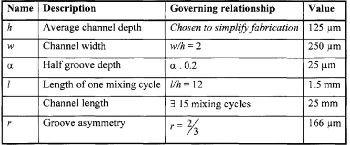
Table 1: Channel dimensions based on mixer publications.
Name Description Governing relationship Value
h Average channel depth Chosen to simpifyfabrication 125 ptm
w Channel width w/h = 2 250 im
a Half groove depth a .0.2 25 ptm
1 Length of one mixing cycle i/h = 12 1.5 mm
Channel length 3 15 mixing cycles 25 mm
Chapter 3: Microfabrication
The two main components of the concentrator - the base containing the electrodes, and the channel with patterned mixing grooves - are fabricated separately and then aligned to each other manually on the die level. Both are microfabricated in a cleanroom by a process that uses mainly photolithography and common MEMS fabrication techniques. The base of the channel is made of Pyrex and contains electrodes patterned in gold. This piece not only serves as the bottom of the channel but also produces the electric fields and provides fluidic access to the device. The channel and chaotic mixer are molded in poly(dimethylsiloxane) (PDMS) using an SU-8 structure. In this chapter, I describe the process I used to fabricate both parts of the device, as well as the packaging that facilitates interfacing between this micro-scale device and its macro-scale inputs and outputs.
3.1 Masks
The two parts - electrodes and channel - of the microconcentrator are fabricated separately and each requires its own set of masks for photolithography. I used one mask to pattern the electrodes and two to pattern the channel: one each for the channel and mixer. All three were 7" chrome masks (Fineline Imaging, Colorado Springs, CO). I chose dimensions for the masks based on the results of the modeling presented in Chapter 2. In this section, I describe some of the key features of these masks in detail.
3.1.1 Electrode Mask
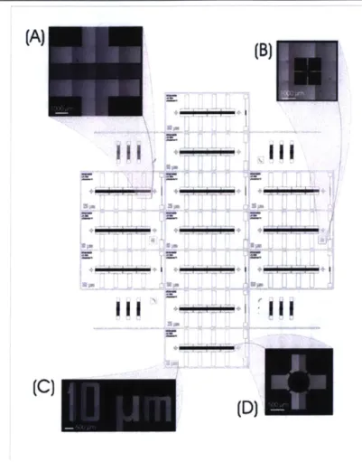
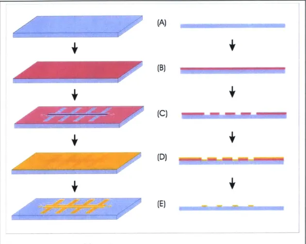
The first mask, used for patterning the electrodes, is shown in Figure 3-1. This is a bright-field mask so that it can be used in a liftoff process. The mask patterns 13 functional dice and contains features designed to simplify fabricating and using the device.
An important design feature of this mask is that the interdigitated electrodes on each die are patterned in four isolated sections, rather than one long section. One such section is shown in Figure 3-la, for 25-ptm electrodes. I used this approach to increase my device yield. Because the resources and facilities I used are intended for research and prototyping, they cannot reliably produce large sets of 10-pLm lines spaced 10 ptm from each other, as required for interdigitated electrodes. Thus, it is likely that at least one pair of adjacent electrodes will be shorted to each
(B)
other. I defined fourisolated sets of
-- electrodes so that if a
pair of electrodes in one section is shorted,
-. . . . the remaining three
still behave as desired. Each of the 13 dice on this wafer has electrodes of 10-, 25-, or 50-pm width and spacing. Building electrodes with a variety of dimensions enabled me to test the characteristic tradeoff
Figure 3-1: Electrode mask between strength and
Background shows an AutoCAD drawing of the mask used reach in the electric for patterning electrodes. Magnifications show: (A) one of field produced by these four sections of 25-pm interdigitated electrodes; (B)
alignment mark; (C) device label; and (D) marker for fluidic electrodes. Each die access hole. Images were acquired by splicing together also contains a resistor several micrographs, giving rise to the variations in shading
across the image. whose width is the
same as that of the
--electrodes on the same die and whose resistance is nominally 100 Q. The purpose of the resistor is to evaluate process parameters, namely the gold thickness or width. Resistances on the 50-pm devices were consistently within 5% of 100 t. Resistances on the 10-pm devices were observed to be less accurate and ranged from approximately 120 n to 250 2.
There are also visual markers on the die- and wafer-level that are not electrically functional. On the die-level, there are crosshairs (Figure 3-id) to indicate the desired location of the fluidic access holes, as well as labels that identify each device (Figure 3-ic). On the wafer-level, there are alignment marks (Figure 3-1b) to enable the addition of a second mask if necessary. I did not use a second mask, but one could be used, for example, to cover only certain areas of the die with a layer of passivation. Also on the wafer-level are dicing streets and resolution features to help assess the quality of the photolithography (shown on SU-8 mask, Figure 3-2e).
3.1.2 SU-8 Masks
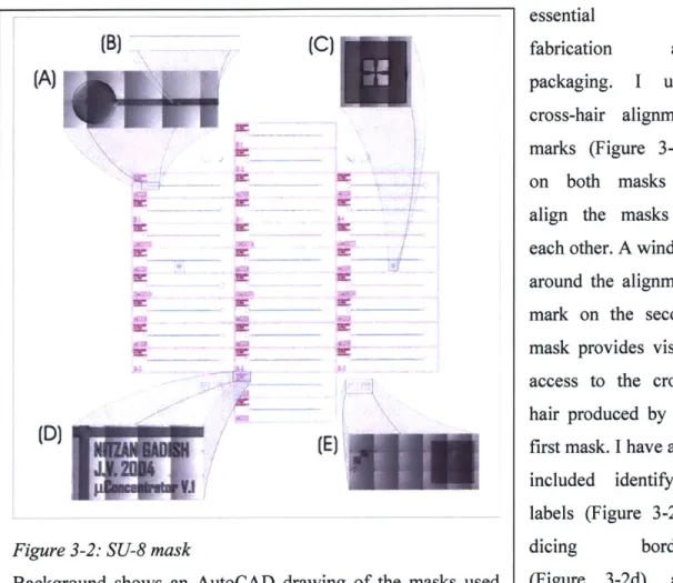
I built the microfluidic channels by means of a molding technique in which microfabricated, raised SU-8 structures are used as a mold to define grooves in PDMS. The SU-8 master mold required two layers of SU-8 patterning: one to define the channel, the other to pattern the mixing grooves. Each layer required one photolithography mask. The two SU-8 masks are shown in Figure 3-2. The first mask (shown in blue) patterns 28 channels all having the same dimensions. The second mask (shown in purple) adds the mixing grooves. Figure 3-2b shows a portion of the two masks in more detail. Both masks are dark-field masks because SU-8 is a negative photoresist.
I included mixing variability in the mask design to facilitate evaluating the effect of the mixer on the device. The mixer mask adds mixing grooves to only some of the channels, while others remain completely smooth (simple channel without mixer). Some of the mixing channels have grooves along the full length of the channel, while some have smooth and mixing sections. In theory, if chaotic flow is detrimental to the holding characteristics of the device, this alternating design should provide sections that circulate
particles and section that trap them. In every channel containing the mixer, the width of the mixing grooves is 5 pm less than that of the channels to provide alignment tolerance.
Similarly to the electrode mask, the SU-8 masks also
(B)
(C)
contain visual markings to essential fabrication and
(A)
4-am,
fi(E)
Figure 3-2: SU-8 mask
Background shows an AutoCAD drawing of the masks used for patterning channels (purple) and mixer grooves (blue). Magnifications show, patterned in SU-8: (A) fluid reservoir and one end of a mixing channel; (B) detail of mask drawing; (C) alignment mark; (D) die label and dicing streets; and (E) features for assessing photolithography. Images were acquired by splicing together several micrographs, giving rise to the variations in shading across the image.
packaging. I used cross-hair alignment marks (Figure 3-2c) on both masks to align the masks to each other. A window around the alignment mark on the second mask provides visual access to the cross-hair produced by the first mask. I have also included identifying labels (Figure 3-2d), dicing borders (Figure 3-2d), and resolution features (Figure 3-2e), all similar to those on the electrode mask.
3.2 Microfabrication Process
I fabricated the concentrator in MIT's Technology Research Laboratory class 100 cleanroom. The fabrication consists of standard MEMS processing and photolithography steps. I have provided a complete outline of the fabrication process in the Appendix, and describe it in detail in the following sections.
3.2.1 Gold Processing
I patterned the electrodes on 6" Pyrex wafers (Bullen Ultrasonics, Eaton, OH) using a gold liftoff process. I chose Pyrex as the substrate because it provides electrical isolation. Due to its low thermal conductivity, Pyrex is sometimes avoided in integrated microfluidic/electronic systems, especially those with biological applications, to prevent overheating bioparticles. At low medium conductivity, however, little power dissipates through the device, thus temperature rises are much less significant. This device is intended for operation with low-conductivity fluid (deionized water), and Pyrex is therefore an appropriate choice.
The liftoff process is a straightforward method of patterning metals that utilizes standard photopatterning and metal deposition techniques and eliminates the requirement of a specific metal (i.e., gold) etchant. In the liftoff process, a uniform layer of the metal is evaporated onto patterned photoresist, which is subsequently dissolved in acetone. The metal in direct contact with the substrate remains, while the metal that was deposited onto photoresist is lifted off when the resist is dissolved.
Figure 3-3 outlines the main steps of the gold liftoff process. I begin the process with blank Pyrex wafers (Figure 3-3a) that I clean for 10 minutes in a Piranha (1:3 H202:H 2SO4) solution to remove organic contaminants, then rinse with deionized water
and spin dry. I dehydrate the wafers (20 mins, 150'C) and then deposit vapor-phase Hexamethyldisilizane (HMDS) onto them at 150'C. HMDS promotes adhesion of photoresist to the substrate. Next, I spin (final speed 3000 rpm) (Figure 3-3b) and pattern (Figure 3-3c) a layer of AZ5214 photoresist using an image-reversal process, such that
the areas to be covered with gold are bare. AZ5214 is a positive resist whose polarity can be reversed via a flood expose. The thickness of the layer of resist is not critical as it serves solely as a mask for gold patterning, but in my case was about 1.7 gm. To pattern the photoresist, I first pre-bake it (30 mins, 90*C), expose (2.3 sec, 10 mW/cm2/sec,
365-405 nm) and post-bake (30 mins, 95*C). I then flood expose the entire wafer (60 sec, 10 mW/cm2/sec, 365-405 nm) to reverse the polarity of the photoresist and finally develop
the resist (70 seconds, AZ 422 developer).
(A)
(B)
-
(C)
-
(D)
(E)
Figure 3-3: Electrode fabrication process
Illustration of the gold liftoff process used to fabricate the electrodes. The process begins with a clean Pyrex wafer (A), onto which photoresist is spun (B). The photoresist is patterned (C) and a layer of gold is evaporated onto it (D). The photoresist is dissolved in acetone, lifting off the gold on top of it and leaving only the desired structures patterned in gold.
I have observed the photolithography process to be very sensitive to both the pre-and post-bake steps. More specifically, changes in temperature during these steps have often resulted in photoresist not developing uniformly across the wafer; that is, there are areas of the wafer in which the resist does not develop. There is a vent in the oven that blows hot air into the chamber to keep it at the desired temperature. I found that baking wafers so that the backsides face the vent prevents this problem.
Following photolithography, I evaporate 100 A of titanium onto the wafer, followed by 2000 A of gold (Figure 3-3d). Titanium promotes adhesion of the gold to the substrate. I soak the wafer in acetone for about 3 hours to remove the photoresist and lift off the unwanted gold. This results in the desired structures patterned in gold on a clean Pyrex substrate (Figure 3-3e).
The final step in this process is to dice the wafer. Prior to dicing, I spin (final speed 500 rpm) and bake
(45 mins, 90*C) a thick,
protective layer of photoresist onto the entire wafer so that die saw slurry does not contaminate the
patterned structures. A I photograph of a
fully-processed die is shown in Figure 3-4: Photograph of a microfabricated Pyrex die Figure 3-4.
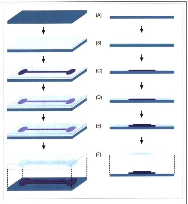
3.2.2 SU-8 Processing
I built the microfluidic channels by molding them in PDMS using a microfabricated SU-8 master mold. SU-8 is a photodefinable, epoxy-based negative resist. Fully patterned SU-8 structures are rigid and durable, and molding is therefore a widely-used technique for patterning microchannels.
I patterned the SU-8 master mold using a two-layer process, illustrated in Figure
3-5, defining the channels in the first layer and the mixer in the second. I carried out the
process on silicon test wafers (WaferNet, San Jose, CA) to minimize cost, as there are no electrical considerations for this process. Following a dehydration bake (30 mins, 200'C) to promote adhesion of the SU-8, I spin the first layer, a 100-ptm layer of SU-8 2050 (MicroChem, Newton, MA) using a final spin speed of 1680 rpm (Figure 3-5b). To pattern, I soft-bake the wafer (15 mins, 95'C), expose it (30 sec, 10 mW/cm2/sec,
365-405 nm) and post-bake (9 mins, 95'C) to harden the SU-8 (Figure 3-5c). Without
developing, I repeat the process for the second layer. This time I spin 50-pLm thick SU-8 2025 (final speed 2250 rpm) (Figure 3-5d), pre-bake (40 mins, 95'C), expose (23 sec, 10 mW/cm2/sec, 365-405 nm), and post-bake (10 mins, 95'C) (Figure 3-5e). I then develop both layers simultaneously (Figure 3-5f) in PM Acetate for approximately 10 minutes (visual stop).
I obtained estimated spin speeds, bake and exposure times for this process from datasheets published by MicroChem
{
#67; #68}. I used these parameters as a starting point for experimentation to achieve the desired results. I used spin speeds lower than those published to achieve 50- and 100-tm-thick layers. Additionally, I baked the second SU-8 layer for significantly longer than the suggested bake times. For example, I increased the prebake time from the suggested 6 minutes to 40 minutes. I did this to adjust for the presence of the first layer, as the MicroChem datasheets are intended for single layer processes.I cast the fabricated mold with PDMS to create the channels (Figure 3-5f). Prior to molding, I silanize the wafer to make it inert to PDMS. Silanization is a vapor-phase deposition of HMDS, performed by placing the wafer and a small volume of liquid-phase HMDS in a vacuum chamber. The HMDS satisfies dangling bonds on the wafer to which PDMS would otherwise bond. I pour a 3-mm layer of PDMS (10:1 base:curing agent by weight) onto the entire wafer and set it to cure at 65'C for about 3 hours. The cured PDMS cleanly peels off the wafer, the desired channel and mixer features having been molded into it by the SU-8. I use a razor blade to cut the PDMS into individual channels.
+
(A) (B)+OPd
0
(C) (D)No
+
+
+
+
(E)+
+
I (F) ISI SI SI SI SI SI 1Figure 3-5: Channel fabrication process
Illustration of key steps in the process used to fabricate the SU-8 master structures used for molding PDMS channels. The process begins with a Pyrex wafer onto which two layers of SU-8 are spun (B, D) and patterned (C, E). Both layers are developed simultaneously and the resulting structure is used for molding PDMS (F).
40por MOMMONNOW"
-Ago&
3.3 Packaging
Packaging provides a way to interface between the micro-scale concentrator and the macro-scale world, and is therefore an essential part of the device design. The concentrator packaging provides external electrical and fluidic access to the device, supplying power to the electrodes and a flow path into and out of the channel. It also holds together the Pyrex base and the PDMS channel. I designed the device with packaging in mind: features such as large bond pads and ample alignment tolerance result
in a simple packaging process that takes about two hours to complete.
3.3.1 Components
I employed a packaging scheme based on that developed in [25]. The package consists of a custom-designed printed circuit board (PCB) (ExpressPCB, Santa Barbara, CA) and an aluminum base, as illustrated in Figure 3-6. The PCB provides electrical access to the device, using a pin and jumper configuration that allows each of the four electrode sections to be turned on or off on the fly. The PCB also provides fluidic access via holes that align with holes in the Pyrex die. Standoffs between the aluminum base and the PCB provide clearance for tubes that route the fluidics into the bottom of the device, so that the tubing does not obstruct optical access to the channel. The aluminum base provides a stable platform for the device. Its magnetic underside, formed by an adhesive magnetic sheet, keeps the device in place on a steel microscope stage. This added steadiness is
electical connectbons PCB PE - tutung electrodes 0 tI-I & channel Aluminum base
valuable for microscope observation of the device during experiments.
I designed the PCB to enable on-the-fly reconfiguration of electrical connections to the device, so that if one section of electrodes is shorted, it can easily be disconnected. The electrical setup consists of three pins on the PCB corresponding to each bond pad on the device (refer to Figure 3-6). The middle pin is connected to the bond pad via a trace in the bottom of the PCB. Of the remaining two pins, one is connected to a voltage and the other to ground, both obtained from the function generator. The middle pin can be shorted to either the voltage or ground pin using a jumper. In this way, each section of electrodes can be turned on by connecting one of its bondpads to a voltage and the other to ground, or off by leaving the bondpads unconnected (or connected at the same voltage). There is also an option to connect the bondpads to two different, non-zero voltages.
3.3.2 Assembly
To assemble the device package, I first prepare the Pyrex die. I drill fluidic access holes according to the markers (Figure 3-1d) using a 0.75-mm-diameter diamond drill bit (C. R. Laurence Co., Inc., Los Angeles, CA). The Pyrex die has a protective coat of photoresist applied prior to dicing the wafer, which I leave as a protective coat for drilling. When the holes are drilled, I rinse the die in a sequence of acetone, methanol, and isopropanol to remove the photoresist.
To minimize nonspecific adhesion of particles to the electrodes during experiments, I coat the Pyrex die with a layer of Sylgard@ Prime Coat (Dow Corning, Midland, MI). The purpose of this surface modification is further explained in Section 4.1.3. I apply the prime coat by dipping the Pyrex die in a diluted solution (10:1 Heptane:Sylgard@ Prime Coat). I submerge the die in the solution for about 10 seconds and then remove it using tweezers, being careful not to let the die reenter the prime coat solution once it is removed. The prime coat dries almost instantaneously, so introducing the die back into the liquid solution would produce a second coating. Only a thin layer of the prime coat is required to minimize nonspecific adhesion, and any additional thickness has the unwanted effect of masking the electric field. After dipping the device in the
prime coat, I let it dry for about 5 minutes. I then pour a few drops of water onto it to verify that the surface is hydrophobic and therefore does not wet.
Next, I populate the PCB with header pins for electrical connections, and then prepare it for attaching the Pyrex die. I use NanoPort adhesive rings (Upchurch, Oak Harbor, WA) to simultaneously affix the die to the PCB and seal the fluidic access holes in the PCB to those in the die. I clean the surface of the PCB with isopropanol and apply the adhesive rings. I then darken the region of the PCB between the fluidic access holes using a black Sharpie marker. This decreases the background fluorescence emitted by the PCB during fluorescence microscopy so that beads, and especially dimmer spores, can be visualized more easily.
To affix the device, I place it on the PCB, aligning corresponding fluidic access holes, and clamp the two together using small binder clips. I use scrap pieces of PDMS to prevent direct contact between the binder clips and the device. I leave this configuration at 65'C for a few hours to let the adhesive set.
I make electrical connections by gluing wires to bond pads on the device using conductive Epoxy (ITW Chemtronics, Kennesaw, GA). I solder the other end of these wires to corresponding through-holes in the PCB. Finally, I pressure-fit PEEK tubing (Upchurch) into the fluidic access holes in the backside of the PCB, and use High Performance Epoxy (Loctite Inc., Rocky Hill, CT) to further seal this connection. I let the Epoxy set at 65'C for about 15 minutes.
Finally, I align a PDMS channel to the electrodes by matching the reservoirs at either end of the channel to the fluidic access holes in the Pyrex die. I set the PDMS on the Pyrex base with a glass slide on top and clamp using large binder clips. Binder clips provide enough pressure to prevent leaking at the desired flowrates and up to about 1000 pl/min. The glass slide aids in distributing the force exerted by the binder clips more evenly along the length of the device. If the force is still uneven and a leak is formed between the PDMS and the Pyrex die, I add another layer of PDMS and another glass
slide to further distribute the force.
I do not use a permanent bond to attach the PDMS to the Pyrex. Over the course of my experiments it has proven beneficial to have the ability to take the device apart, for purposes of thorough cleaning or replacing the channel. A more permanent bond would
necessitate a lengthy cleaning process to strip the PDMS off the Pyrex, and moreover, the PDMS would not be reusable. However, while a temporary seal is suitable for prototyping, a more permanent bond could be used in the final device design. The Pyrex die is coated with a layer of Sylgard@ Prime Coat to which PDMS bonds when both surfaces are treated with oxygen plasma. This would eliminate the need to clamp the device components together.
The packaged device can be unpackaged and all the parts reused. The PDMS is not permanently bonded to the die, thus is easily removed from the package. I soak the remaining components of the package (PCB, Pyrex die, tubes) in acetone for about an to softens the Epoxies and NanoPort adhesives. This allows me to remove the Pyrex die and PEEK tubes from the PCB. I use a razor blade to remove the High Performance Epoxy from the back of the PCB. Acetone removes the conductive epoxy from the wires that connect to the bond pads. These wires are soldered in to the PCB and can be reused. To remove the Sylgard Prime Coat from the Pyrex die, I soak the die in KOH (100 mg/mL DI water; VWR, Westchester, PA) for at least 4 hours. I remove the die from the KOH and immediately rinse it in heptane (anhydrous 99%; Sigma-Aldrich, St. Louis, MO). The prime coat can then be reapplied and the die repackaged using the same PCB.