www.advmatinterfaces.de
Full PaPer
Carbon-Assisted Stable Silver Nanostructures
S. Narjes Abdollahi, Efraín Ochoa Martínez, Cédric Kilchoer, Geoffroy Kremer, Thomas Jaouen,
Philipp Aebi, Tim Hellmann, Thomas Mayer, Yibei Gu, Ulrich B. Wiesner, Ullrich Steiner,
Bodo D. Wilts, and Ilja Gunkel*
DOI: 10.1002/admi.202001227
1. Introduction
Plasmonic nanostructures based on gold or silver are of great interest as functional materials with applications in the fields of health[1] and energy,[1,2] as catalysts[3] and metamaterials.[4] While nanostruc-tured gold is most commonly used in plasmonic applications, its replacement with silver is highly desirable because this reduces optical losses in the visible spectral range.[5] The use of nanostruc-tured silver is however limited by its low stability under ambient conditions, where it rapidly degrades,[6,7] particularly in high humidity[8] and under light illumination.[9]
The degradation of silver nanostruc-tures can in principle be reduced by contacting silver with a sacrificial metal[10] or by applying a protective inorganic[11–13] or organic[14,15] layer around the silver nanostructure. Such a layer alters however the optical response of the uncoated nanostructure by changing its dielectric envi-ronment.[16,17] Alternatively, silver can be passivated without applying protective layers by using hydrogen plasma pro-cessing,[18] or under an argon atmosphere.[8,19] These passiva-tion methods are, however, limited to only a few nanostructures or require the control of the environment the nanostructures are exposed to. The stabilization of complex silver nanostruc-tures has not yet been achieved and overcoming optical losses remains a challenge in the field of nanoplasmonics.[20]
The polymer template-assisted fabrication of 3D metallic nanostructures is useful to generate metals with complex and well-ordered morphologies.[21] This bottom-up manufacturing route typically employs block copolymers, chemically dis-tinct, covalently linked polymer blocks that can self-assemble into intricate 3D nanostructured morphologies such as the gyroid.[22] Metal replica of these morphologies can be produced by electrochemical and electroless plating of metals into a voided polymer template, generated by selective etching.[21,23,24] To create a free-standing metal replica, the remaining polymer template is typically removed by harsh etching or polymer deg-radation procedures, which are not suitable for degdeg-radation- degradation-sensitive materials such as nanostructured silver.
Here, we demonstrate the long-term stabilization of silver nanostructures, grown inside a voided polymer template, by using argon plasma etching at ambient temperatures. Following a polymer template-assisted fabrication route that was previ-ously developed for the manufacture of gold,[25] nickel,[26] and platinum gyroid nanostructures,[27] we demonstrate how similar
Nanostructured silver stands out among other plasmonic materials because its optical losses are the lowest of all metals. However, nano-structured silver rapidly degrades under ambient conditions, preventing its direct use in most plasmonic applications. Here, a facile and robust method for the preparation of highly stable nanostructured silver mor-phologies is introduced. 3D nanostructured gyroid networks are fabricated through electrodeposition into voided, self-assembled triblock terpolymer scaffolds. Exposure to an argon plasma degraded the polymer and stabi-lized the silver nanostructure for many weeks, even in high humidity and under high-dose UV irradiation. This stabilization protocol enables the robust manufacture of low-loss silver nanostructures for a wide range of plasmonic applications.
S. N. Abdollahi, Dr. E. Ochoa Martínez, Dr. C. Kilchoer, Prof. U. Steiner, Dr. B. D. Wilts, Dr. I. Gunkel
Adolphe Merkle Institute University of Fribourg
Chemin des Verdiers 4, Fribourg CH-1700, Switzerland E-mail: [email protected]
Dr. G. Kremer, Dr. T. Jaouen,[+] Prof. P. Aebi
Département de Physique and Fribourg Center for Nanomaterials Université de Fribourg
Fribourg CH-1700, Switzerland T. Hellmann, Dr. T. Mayer
Department of Materials and Earth Sciences Surface Science Laboratory
Technical University of Darmstadt
Otto-Berndt-Strasse 3, 64287 Darmstadt, Germany Prof. Y. Gu,[++] Prof. U. B. Wiesner
Department of Materials Science and Engineering Cornell University
330 Bard Hall, Ithaca, NY 14853-1501, USA
The ORCID identification number(s) for the author(s) of this article can be found under https://doi.org/10.1002/admi.202001227. © 2020 The Authors. Advanced Materials Interfaces published by Wiley-VCH GmbH. This is an open access article under the terms of the Creative Commons Attribution License, which permits use, distribution and reproduction in any medium, provided the original work is properly cited.
The copyright line for this article was changed on 10 November 2020 after original online publication.
[+]Present address: Univ Rennes, CNRS, Institut de Physique de
Rennes - UMR 6251, Rennes F-35000, France
[+]Present address: TeraPore Technologies, Inc., 407 Cabot Road, South
www.advancedsciencenews.com
www.advmatinterfaces.de
nanostructured silver morphologies can be rendered stable against degradation, without the need for thick coating layers.
2. Results and Discussion
2.1. Fabrication and Structural Characterization
Here, we generalize the fabrication of 3D metal nanostruc-tures via the templated deposition of metals into voided block copolymer films, from stable nanostructured Au to degradation-sensitive Ag nanostructures, schematically shown in Figure 1. In brief,[25] 3D nanostructured polymer templates were prepared by spin coating gyroid-forming
polyisoprene-b-polystyrene-b-polyethylene oxide (ISO) triblock terpolymer
films onto fluorinated tin oxide (FTO)-coated glass substrates, followed by selectively removing polyisoprene by a combination of UV exposure and immersion in ethanol. The voided polymer films were then backfilled with Ag (or Au) by electrodeposition, thereby replicating the polymeric nanostructure into the metal. Free-standing metal replica were manufactured by removing the sacrificial polymer template through plasma etching, a commonly used technique to remove organic residues from surfaces at ambient temperature.[28] We show that plasma etching using inert Ar gas allows the stabilization of nanostruc-tured silver networks despite their strong tendency to degrade.
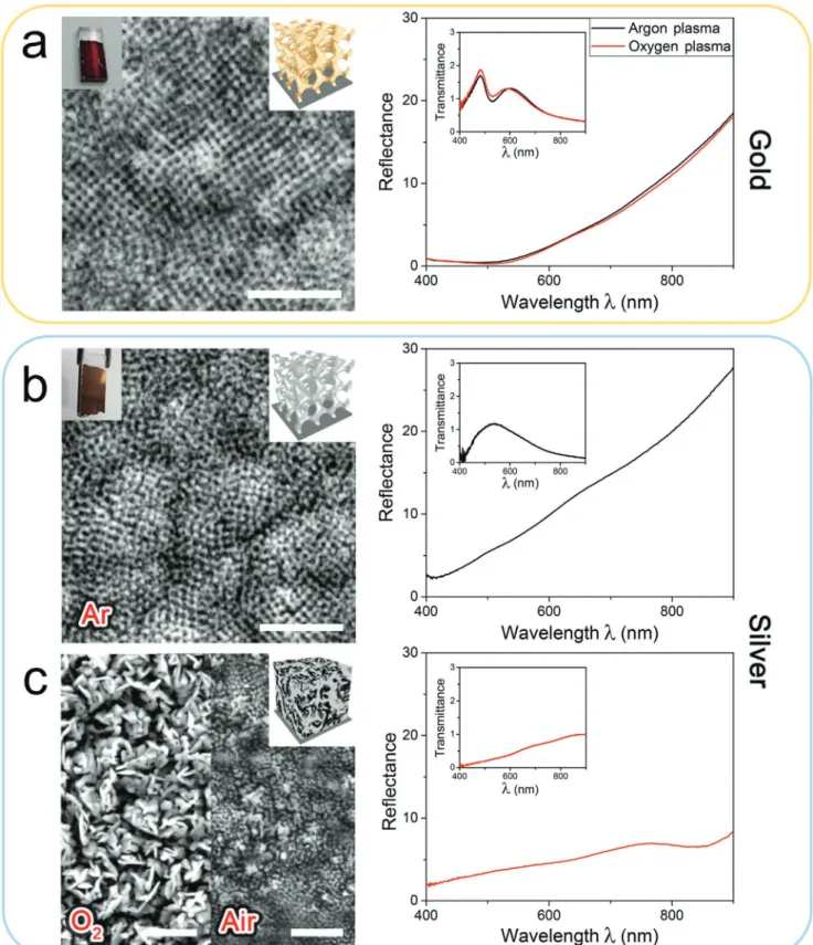
The scanning electron microscopy (SEM) images in Figure 2 confirm that Ar-etched Ag gyroids (Figure 2b) look structurally
identical to the Au reference samples etched with any plasma (Figure 2a), while the gyroid structure in silver samples etched with O2 or air plasmas were substantially degraded (Figure 2c). Reflectance and transmittance spectra of the resulting free-standing replica (Figure 2, right column) are spectrally similar, with prominent reflectance minima at 500 nm (Au) and 410 nm (Ag). The blue-shifted optical response for Ag is expected due to the different plasma wavelength of bulk Ag compared to that of Au.[29] Etching the Ag network with air or O
2 results in a broad and essentially featureless reflectance, implying the loss of structure, which likely results from the degradation of Ag upon etching with reactive process gases.
2.2. Chemical Composition of Ag Gyroid Replica
2.2.1. Surface Analysis Using X-Ray Photoelectron Spectroscopy
X-ray photoelectron spectroscopy (XPS) was used to analyze the chemical composition of the Ag gyroids manufactured by Ag electrodeposition into voided ISO terpolymer films on FTO-coated glass substrates, followed by Ar plasma etching (Figure 3). The strongest peaks in the XPS survey spectra of the manufactured Ag gyroids coincide with those of an Ag refer-ence surface. These peaks are significantly stronger than addi-tionally observed K 2p, C 1s, and O 1s peaks, indicating that the gyroid replica mostly consists of Ag (Figure 3a). The small Mo 3d peak in the Ag reference spectra indicates molybdenum
Figure 1. Schematic diagram of the sample fabrication.[25] a) Starting from a voided ISO triblock terpolymer template, b) Au (top) or Ag (bottom) are
electrodeposited into the voided network. c) The polymer template is then removed by plasma etching, resulting in a free-standing, metallic gyroid replica. For Ag, only Ar plasma etching results in a stable nanostructure, while for gold any plasma (Ar, O2, or air) can be employed.
www.advancedsciencenews.com
www.advmatinterfaces.de
Figure 2. Morphology and optical properties of free-standing metal gyroid networks after plasma etching using different gases. a) SEM image of an O2
plasma-etched Au gyroid and optical reflectance and transmittance spectra for Au gyroids plasma-etched with either Ar or O2. The Ar plasma-etched Ag
gyroid in (b) exhibits a very similar nanostructured morphology and optical spectra as the Au gyroid in (a). c) Upon O2 or air plasma etching, however,
the nanostructured Ag morphology was substantially degraded and its optical reflection spectrum shows no resemblance to that of a structured Ag film. The reflectance spectra in (a) and (b) have minima, at ≈410 nm (Ag) and ≈500 nm (Au), which can be attributed to the different plasma wavelengths of these two metals. Scale bars: 500 nm.
www.advancedsciencenews.com
www.advmatinterfaces.de
contamination. The K 2p peak in the Ag gyroid survey spectra is most likely related to KOH, which is an ingredient in the Ag plating solution used for electrodeposition. The compounds associated with the C 1s and O 1s peaks in the survey spectra of the Ag gyroid (Figure 3a) are discussed in more detail below. The intensity of these peaks significantly reduces upon Ar sput-tering of the Ag gyroid replica as shown in the corresponding XPS survey spectrum (Figure 3a). This implies that there is a low concentration of oxygen- and carbon-containing com-pounds located at the gyroid surface.
A detailed analysis of the Ag 3d peaks in high-resolution XPS spectra (Figure 3b,c; Figure S1a, Supporting Information) reveals that the binding energies and corresponding full-width at half-maximum (FWHM) values of the Ag gyroid peaks match those of a Ag reference surface (Figure 3d), as well as literature
values for metallic Ag0. The Ag 3d
5/2 peak analysis also revealed traces of an oxidized silver species in the Ag replica, the amount of which is extremely low (<6 %, Figure S2, Supporting Infor-mation) and stable even under harsh environmental conditions (see below). These findings confirm the predominantly metallic nature of the Ag gyroid replica.
The compounds associated with the carbon and oxygen con-tributions in Ar plasma-etched Ag gyroids were investigated by analyzing high-resolution O 1s and C 1s XPS spectra of the Ag gyroid and the polymer template used for its fabrication (Figure 4). The O 1s spectra of the polymer template (Figure 4a) and the Ag gyroid (Figure 4c) are evidently different, which implies distinct chemical states. The O 1s peaks observed for the polymer template (Figure 4a) correspond to COC bonds at 531.05 eV and COH at 532.78 eV in a PEO-containing
Figure 3. Chemical composition of Ag gyroids manufactured by metal deposition into a voided polymer template and subsequent Ar plasma etching.
a) XPS reference spectra of a Ag surface (gray) and a voided ISO gyroid terpolymer template (black), compared to the spectra of an Ar plasma-etched Ag gyroid (blue), and the same plasma-etched Ag gyroid after an additional Ar sputtering inside the XPS vacuum chamber (red). b) Fit (shaded region) of the Ag 3d region to an Ar plasma-etched Ag gyroid high-resolution XPS spectrum. The sum of the individual fits coincides with the measured spectra and is therefore not shown. c) High-resolution Ag 3d spectra of an Ar plasma-etched Ag gyroid (blue) and the same sample after additional Ar sput-tering (red). The insets show magnifications of the plasmon loss (PL) regions corresponding to Ag 3d5/2 and Ag 3d3/2. d) Summary of the binding
www.advancedsciencenews.com
www.advmatinterfaces.de
sample (the polymer template consists of cross-linked PS and PEO, see Figure 1).[30,31] The peaks in the O 1s spectrum of the Ag gyroid replica (Figure 4c) instead were assigned to AgO bonds in oxidized silver at 530.55 eV and KOH bonds in KOH at 531.10 eV. The additional O 1s peaks for the Ag gyroid replica correspond to CO bonds at 532.02 eV and CO at 533.22 eV both associated with adventitious contamination, resulting from either polymer degradation during Ar etching at medium vacuum (0.2 mTorr) in the plasma chamber, or air exposure once the samples are removed from the chamber.[32]
At lower binding energies, the potassium contamination shows K 2p peaks at 293.09 and 295.99 eV. The dominant carbon peak in the Ag gyroid C 1s spectrum (Figure 4d) was assigned to CC bonds of either adventitious or amorphous carbon[33] at 284.67 eV. The additional C 1s peaks of the Ag gyroid spectrum correspond to CO bonds at 285.58 eV and CO bonds at 287.68 eV, both of which are associated with adventitious contamination. This is consistent with the O 1s spectrum of the same sample (Figure 4c). In contrast, the carbon peaks observed in the high-resolution XPS C 1s spectra of the voided polymer template (Figure 4b) were assigned to CC
bonds of aromatic carbon in PS at 283.87 eV,[34] CC bonds at 284.88 eV of adventitious carbon or PS cross-links, CC and CH bonds in both PS and PEO at 285.73 eV,[30,35] CO bonds in PEO at 287.44 eV,[36] and a π–π* satellite at 292.43 eV.[34,35] This confirms that the contaminations observed on the surface of Ar plasma-etched Ag gyroids are chemically different from the polymer template used for its fabrication. The dominant CC peak at 284.67 eV is particularly notable and may pro-vide an explanation for the Ag stabilization as discussed below (see Discussion).
While adventitious contamination is inevitable for cleaned, high-surface-energy, metallic samples once they are exposed to ambient atmosphere,[32] such contamination can be removed, for example, by Ar sputtering. The carbon and oxygen peaks associated with adventitious contamination seen in the high-resolution XPS C 1s and O 1s spectra of an Ar plasma-cleaned Ag gyroid diminish upon Ar sputtering the sample inside the XPS vacuum chamber (Figures S1b–e and S2, Supporting Information). While the amount of amorphous carbon on the Ag gyroid surface also reduces upon Ar sputtering, it remains the dominant contribution in the corresponding C 1s spectra
Figure 4. XPS analysis of carbon and oxygen contamination on Ag gyroid surfaces. High-resolution XPS spectra of the O 1s and C 1s regions of a,b) a
voided ISO gyroid terpolymer film and c,d) an Ar plasma-cleaned Ag gyroid. The colored shading corresponds to fits assuming binding energies of the indicated bonds.
www.advancedsciencenews.com
www.advmatinterfaces.de
(Figures S1e and S2, Supporting Information). Ar sput-tering reduced the amount of oxidized Ag to less than 1% (Figures S1a,d and S2, Supporting Information). The positions of the K 2p peaks of the Ar plasma-cleaned Ag gyroid shift to higher binding energies upon Ar sputtering while the FWHM values of both potassium peaks slightly decrease upon cleaning the surface. This implies that potassium, unlike the organic contamination as well as most silver oxide traces, is incorpo-rated in the Ag gyroid network.
2.2.2. Volumetric Analysis Using Secondary Neutral Mass Spectrometry
Secondary neutral mass spectrometry (SNMS) was employed to obtain chemical information across the entire thickness of Ag gyroid replica, thereby complementing XPS (Figures 3 and 4), which only probes the top surface of the sample. To this end, SNMS and cross-sectional focused-ion beam-scanning elec-tron microscopy (FIB-SEM) imaging were used to characterize both a Ag gyroid replica inside a voided ISO terpolymer film (Figure 5a,b) and a free-standing Ag gyroid, where the polymer template was removed by Ar plasma etching (Figure 5c,d). The
SNMS depth profiles of both samples, that is, before and after removal of the polymer template by plasma etching indicate that Ag as well as C are (homogeneously) present across the entire thickness of the films. This is consistent with the XPS results, where adventitious contamination was observed on Ar plasma-etched Ag gyroids. No oxygen was detected by SNMS.
Ar plasma-etched Ag gyroids were additionally characterized by energy-dispersive X-ray spectroscopy (EDS) and X-ray dif-fraction (XRD) to confirm their chemical nature and structure (Figure S3, Supporting Information). The EDS analysis con-firms that the gyroid sample contains Ag, C, and O. The XRD pattern of a an Ar plasma-cleaned Ag gyroid corresponds to that of metallic Ag0. This confirms the crystalline nature of the metallic Ag0 gyroid replica.
2.3. Long-Term Chemical and Photophysical Stability
Exposure of Ag nanostructures to humidity and UV irradiation eventually destroys the nanostructured morphology, restricting their technological application. The surface of Ag nanostruc-tures gradually reacts with atmospheric oxygen and sulfur, significantly changing the material’s optical properties, often
Figure 5. Volumetric composition of Ag gyroid replica. a) Focused-ion beam cross-sectional images of a Ag gyroid replica inside an ISO terpolymer
template and c) a free-standing Ag gyroid replica, where the polymer template was removed by Ar plasma etching. In both samples Au-coated Si wafers were used as substrates. The samples were protected by sputtered-on Pt layers to avoid charging and degradation during SEM imaging. For the Ag gyroid inside the voided ISO terpolymer template in (a), electrodeposition was stopped before filling the entire thickness of the template (thickness of unfilled template ∼200 nm). Scale bars are 500 nm. Secondary neutral mass spectrometry (SNMS) analysis of samples b) before and d) after Ar plasma treatment corresponding to the samples shown in (a) and (c), respectively. Contributions of C, O, Ag, and Au are shown as a function of the sputtering time, resulting from sputtering the samples in the vertical direction starting from the top surface.
www.advancedsciencenews.com
www.advmatinterfaces.de
over the course of a single day.[7,37] To determine whether the Ar plasma-etched Ag samples are stable against such external factors and environmental effects, we exposed a series of sam-ples to different degrees of humidity and light irradiation for long periods of time, and measured their optical response and morphology (Figure 6).
We investigated the stability of Ar plasma-etched Ag replica under standard laboratory conditions (RH 35–40%) and in a water vapor-saturated atmosphere (RH = 99%) for up to 30 days (Figure 6a–d). The morphology and the spectral response were monitored every few days. Figure 6a,c shows the stability of the nanostructured morphology with no discernible deterioration over 30 days. Furthermore, the spectral reflectance changed only very slightly over time (Figure 6b,d). The continued storage of samples under ambient laboratory conditions for over 2 months did not induce any changes in morphology or spectral response (not shown). In contrast, the appearance and morphology of air plasma-etched Ag gyroid replica changed rapidly (Figure S4, Supporting Information). These results clearly demonstrate that the Ar plasma-etched Ag nanostruc-tured networks are stable in humid environments, even under RH as high as 99%, much higher than previously reported.[8,38]
Further, previous studies found that the use of Ag nanostruc-tures for applications is severely limited due to photodegrada-tion.[39–41] To investigate the light stability of Ar plasma-etched Ag nanostructures, additional samples were exposed to white light that included the UVA/UVB spectral range. In a further sample series, illumination was carried out employing a UV-absorbing spectral filter that removed the UV spectral range. The optical response and sample morphology were monitored over 5 days of continuous illumination. Figure 6e,f shows that long-term illumination with visible light (no UV) influenced neither the nanostructured Ag gyroid morphology nor the spectral response. More surprisingly, the Ag gyroid was also
resilient to long-term illumination that included a strong UV component (Figure 6g,h). This is in strong contrast to pre-vious studies that showed immediate changes in Ag nanostruc-tures upon exposure to even low intensities of white light,[42] demonstrating the effectiveness of Ar plasma etching on the stability of nanostructured Ag.
2.4. Discussion
Our results show that Ag nanostructures can be stabilized against degradation through Ar plasma etching, which keeps the metallic nature of Ag intact even under harsh environ-mental conditions such as high humidity and UV illumination. Similar to previous results, in which the Ag surface was cov-ered by a polymer shell to avoid degradation due to tarnishing,[14] our Ag nanostructures were created by electrodepositing Ag into a polymer template (Figure 1) that surrounded and prob-ably protected Ag from degradation before the Ar plasma treat-ment takes place. While plasma etching is a common technique to remove organic materials through interactions with a reactive process gas,[28] our results show that the choice of process gas is essential to maintain the Ag nanostructure (Figure 2). The reactive plasma of O2 or air destroys the nanostructured mor-phology (Figure 2), while an inert Ar plasma ablates organic res-idues in a nonreactive manner.[28,43] This not only maintains the Ag nanostructure during the etching process but also makes it highly resistant against exposure to environments that typically require additional surface passivation. The amount of silver oxide that is detected by XPS is negligible and probably local-ized in individual patches rather than a conformal layer.
The analyses in Figures 3–5 demonstrate that the polymer template is entirely degraded by the plasma etching step and the pure metallic nature of the Ag gyroid is confirmed, with
Figure 6. Stability of Ar plasma-etched Ag gyroids against a–d) humidity and e–h) UV irradiation. a,c,e,g) SEM micrographs of the Ag gyroid network
before and after extended exposure to different environments. Samples were stored in a laboratory environment with a,b) a relative humidity of ≈40% and c,d) a relative humidity of ≈99% for up to 30 days. A second sample series was exposed to light e,f) without and g,h) with UVA/UVB components for up to 120 h. b,d,f,h) Time-dependent reflectance spectra. Scale bars: 500 nm.
www.advancedsciencenews.com
www.advmatinterfaces.de
additional low concentrations of amorphous carbon and adventitious contamination.
To arrive at a hypothesis for the robust stabilization of the silver gyroids, we summarize the following observations: 1) Stable nanostructured Ag morphologies are achieved by the combination of Ar plasma etching and the presence of a polymer template surrounding the Ag gyroid that is etched by the plasma; 2) the presence of CC bonds in amorphous carbon at 284.67 eV,[33] which is different from the peaks observed for the voided polymer matrix; 3) carbonaceous layers such as graphite or graphene are known to stabilize Ag and other metal surfaces against degradation[15,41,44–46]; and 4) polystyrene is known to graphitize when degraded by an Ar plasma.[47–49]
Based on these four statements, we formulate a possible stabilization mechanism of the nanostructured Ag gyroid morphology. During the removal of the polymer matrix by Ar plasma etching, amorphous CC skeletons are formed pre-dominantly from the degradation of polystyrene. Since the plasma etching process takes place in medium vacuum, it is likely that these carbonaceous fragments strongly physisorb onto the Ag surface. Based on earlier studies,[15,41,44–46,50] we speculate that such a physisorbed carbonaceous layer (which may be molecularly thin) is responsible for the resilience of our nanostructured silver gyroid against degradation (Figures 6 and Figure S3, Supporting Information).
This hypothesis is motivated by earlier work that shows an adsorbed graphene layer not only protects an underlying Ag surface, but even reduces already formed Ag oxides.[46] Because of the high surface energy of bare metals, such a physisorbed layer can be very strongly attached to the Ag surface, thereby accounting for the extraordinary stability of the underlying Ag. Such a layer further impedes photodegradation by limiting photo-induced Ag+ ion formation, increased light absorption, and improved heat conduction.[41,51] A proof of the presence of such a layer and its detailed chemical composition requires however a careful surface physics study of equivalent Ag model surfaces, which is beyond the scope of the present work. The observation of a stabilizing carbonaceous layer is further related to the CASH method[52] for the block copolymer directed for-mation of highly crystalline oxide materials. In CASH, sp2 -hybridized carbon-containing polymers (such as polystyrene) form carbonaceous materials under heating in non-oxidizing environments (e.g., Ar gas).
Our approach to create stable nanostructured Ag morpholo-gies is particularly valuable for Ag-based nanoplasmonics and metamaterials. This is demonstrated in a separate publica-tion, where we have investigated the metamaterial properties of large-domain, nanostructured Ag gyroid samples that were stabilized by Ar plasma etching as introduced in the present study,[53] revealing significantly enhanced metamaterial proper-ties (i.e., circular dichroism), due to lower losses compared to metamaterials made of Au.
3. Conclusion
We have discovered a process for manufacturing nanostruc-tured Ag that is stable in harsh environments that otherwise
lead to its rapid degradation and structural loss. The combination of XPS results and stability measurements point toward the formation of a very thin graphitic layer covering the Ag surface upon Ar etching, which resulted from etching the (predominantly polystyrene-containing) polymer template surrounding the Ag with an Ar plasma. We hypothesize that, similar to graphene, this very thin graphitic layer stabilizes Ag against degradation.
This approach allows generating stable Ag nanostructures of various morphologies and sizes by adjusting the composition and molar mass of the block copolymer template used for fab-rication. Alternatively, existing Ag nanostructures of arbitrary shape can be stabilized against degradation by surrounding them with a suitable polymer that is subsequently degraded and partially graphitized by Ar plasma etching. Tunable Ag nanostructures that are stable in ambient conditions under illu-mination are particularly valuable in the field of plasmonics, where its low plasmonic losses make it preferred over Au, which is currently predominantly used because of its superior stability. This study not only paves the way for the wide-spread use of nanostructured Ag as plasmonic metal, it lends itself to the extension to further corrosion-sensitive metallic nanostruc-tures, such as Cu, Ni, or Pt, with the goal to enable their long-term stability for a range of applications.
4. Experimental Section
Sample Fabrication: Polyisoprene-b-polystyrene-b-polyethylene
oxide (PI-b-PS-b-PEO, ISO) triblock terpolymer with a molar mass of 80 kg mol−1 and volume fractions of f
PEO = 17 %, fPI =30 %,
and fPS =53 % was prepared by anionic polymerization as described
elsewhere.[54,55] FTO-coated glass (Sigma) and Au-coated Si wafers
(100 nm thick Au layer grown by physical vapor deposition) were used as substrates for ISO terpolymer films, and cleaned by immersion in acetone (Sigma) and isopropanol (Sigma) prior to coating. FTO-coated glass substrates were additionally cleaned with Piranha (3:1% v/v mixture of H2SO4 and 30% H2O2) solution, and subsequently silanized
by immersion in a 0.2% v/v solution of trichloro(octadecyl)silane (Sigma) in cyclohexane (Sigma) for about 10 s.
ISO terpolymer films atop FTO-coated glass or Au-coated Si substrates were prepared by placing a 25 μL drop of a 10 wt% solution of ISO terpolymer in anhydrous anisole (Sigma) onto the substrate, followed by spin coating for 60 s at 1200 rpm with an acceleration of 500 rpm using a WS-650Mz-23NPPB (Laurell Technologies) spin coater. The films were not annealed, which is known to limit the size of gyroid grains in ISO terpolymer films.[56] To create polymer templates for metal
electrodeposition, the PI phase in as-spun ISO terpolymer films was degraded by UV irradiation for 15 min (15 W, peak emission at 254 nm, sample-to-light source distance 11 cm (Analytik Jena, UV bench lamp GZ-97605-05)) and subsequently removed by immersion of the film in ethanol (Sigma) for 30 min.
To create metal gyroid replica, the voided network in the polymer template was backfilled with metal by electrodeposition using a Metrohm AutoLab PGSTAT302N potentiostat and either Ag plating solution (MetSil 500CNF, Metalor) or Au plating solution (ECF 60, Metalor) with 0.5% v/v brightener (a 66.7 mM As2O3 (Sigma) solution in
DI H2O with KOH added to adjust the pH to about 14). A three-electrode
cell was employed with FTO-coated glass as the working electrode, a Pt electrode tip (Metrohm) as the counter electrode, and a Ag/AgCl with KCl reference electrode (Metrohm). Metal was electrodeposited by cyclic voltammetry within a potential range of −0.4 to −1.15 V at a scan rate of 0.05 V s−1 (for both Au and Ag), followed by applying a constant
www.advancedsciencenews.com
www.advmatinterfaces.de
After electrodeposition, the remaining PEO and PS phases surrounding the metal gyroid replica were degraded by plasma etching using a PE-100-RIE Plasma Etch Inc. system equipped with a process temperature controller. The samples were etched in either Ar, O2, N2, or
air for 20 min, at 50 W power and 40 sccm flow rate, while maintaining the sample temperature at 5 °C.
Structural Characterization: Scanning electron micrographs were
obtained using a Tescan Mira3 LM field-emission scanning electron microscope (Tescan, Brno, Czech Republic) operating at 5.0 kV. Cross-sectional images were obtained using an FEI Scios 2 (FEI, Eindhoven, The Netherlands) dual-beam field-emission electron microscope equipped with a gallium-ion ion beam (operated at 30 kV, 0.5 nA).
Optical Characterization: The reflection spectra of samples were
measured using a ZEISS Axio Scope.A1 optical microscope (Germany), with a 100 W halogen lamp and a 5× Zeiss Neofluar objective (NA = 0.1). The microscope features an optical fiber (QP230-2-XSR-BX, Ocean Optics) that was positioned in a confocal plane with respect to the image plane. Spectra were then measured using an Ocean Optics QEPro spectrometer (Ocean Optics, Dunedin, FL).
For continuous reflection measurements, a bifurcated optical probe (Ocean Optics QR400-7-UV-BX) was employed and connected to an AvaLight-DH-S-BAL Deuterium-Halogen (Avantes, Eerbeck, The Netherlands) light source and an Ocean Optics Flame-T spectrometer. To filter out UV light, an absorptive gray-filter (ND = 2, NE20B; Thorlabs, Ely, UK) was placed between the light source and optical fiber.
Energy-Dispersive X-Ray Spectroscopy: EDS spectra were measured
using an Oxford Aztec Advanced system (United Kingdom) equipped with an XMAX 150 mm2 silicon drift detector at an acceleration voltage
of 20 kV.
X-Ray Diffraction: XRD patterns were collected on a Rigaku Ultima IV
diffractometer (Japan) using CuKα radiation (λ = 1.5418 Å). FTO-coated
glass was used as the substrate for the measurement.
X-Ray Photoelectron Spectroscopy: XPS measurements were carried
out at the Physics Department of the University of Fribourg and the Integrated System for Solar Cell Research (DAISY-SOL) at the University of Darmstadt. The XPS measurements at the University of Fribourg were performed using a monochromatized Al Kα (1486.6 eV) X-ray
source (SPECS μ–FOCUS, resolution ≈ 300 meV) and a Scienta DA30
photoelectron analyzer. Survey spectra were acquired with a pass energy of 200 eV, an energy step of 0.5 eV, and a dwell time of 500 ms. For high-resolution spectra, the measurements were carried out with a pass energy of 100 eV, an energy step of 0.04 eV, and a dwell time of 500 ms. The XPS measurements at DAISY-SOL were performed using a Thermo Fisher Escalab 250 system equipped with an X-ray source providing monochromatic Al Kα radiation. All spectra were acquired with a pass
energy of 10 eV, a step size of 0.05 eV, and a dwell time of 50 ms per measurement point. For the calibration, the Fermi edge of Ag (0 eV) as well as the Au 4f7/2 (84.0 eV), Ag 3d5/2 (368.26 eV), and the Cu 2p3/2
emission lines (932.67 eV) of sputter-cleaned metal surfaces were used. Prior to the measurements, the sample surface was cleaned by 5 min of Ar sputtering inside the XPS chamber at an acceleration voltage of 3 kV and a 45° incident angle with respect to the sample surface. Peaks were fitted using the CasaXPS software assuming a convolution of a Gauss and a Lorentz peak after applying a Shirley background subtraction. Peaks were assigned using to binding energy values from standard databases[57,58] unless otherwise noted.
Secondary Neutral Mass Spectrometry: Depth profiles of the samples
were obtained by SNMS (INA-X, SPECS GmbH, Berlin) in high-frequency mode by sputtering with Ar+ ions of 200 eV. The RF plasma
was coupled inductively by a Dressler Cesar 600. The effective power was 125 W (150 W forward power and 25 W reflected power). Two Helmholtz coils provided a magnetic field of 10 G A−1 with 3 A current in parallel
connection to achieve cyclotron resonance conditions for efficient post ionization of the sputtered neutrals. Samples were mounted on a Cu sample holder with a Ta mask pressing the sample to the support. The Ta mask further ensured confining the erosion area to a circle of 2 mm diameter. All experiments were run with a 7.5 mm Mo aperture as entrance to the plasma chamber.
Supporting Information
Supporting Information is available from the Wiley Online Library or from the author.
Acknowledgements
The authors thank Esteban Bermúdez-Ureña (Adolphe Merkle Institute), Shanti Bijani (Centro SCBI-Bioinnovación, Universidad de Málaga), Christoph Neururer (University of Fribourg), Justin Llandro (Tohoku University), and Nathan Fuchs (University of Fribourg) for their valuable help with this work. This research was supported through the Swiss National Science Foundation through grant numbers 163220 and 188647 (to U.S.) and 168223 (to B.D.W.), the National Center of Competence in Research Bio-Inspired Materials (to U.S., B.D.W., and I.G.), and the Adolphe Merkle Foundation. E.O.M acknowledges support from the Marie Skłodowska Curie fellowship, H2020 Grant agreement no. 841005, project PerSiSTanCe. T.H. and T.M. acknowledge funding by the German Research Foundation (DFG) under the project title “Inverted non-fullerene organic solar cells” project number 196886395. U.B.W. thanks the National Science Foundation for support (DMR-1707836).
Conflict of Interest
The authors declare no conflict of interest.
Keywords
3D plasmonic nanostructures, argon plasma treatment, graphitic layers, long-term stability, silver nanostructures
Received: July 9, 2020 Revised: September 13, 2020 Published online:
[1] D. J. de Aberasturi, A. B. Serrano-Montes, L. M. Liz-Marzán, Adv.
Opt. Mater. 2015, 3, 602.
[2] K. Ueno, T. Oshikiri, Q. Sun, X. Shi, H. Misawa, Chem. Rev. 2018,
118, 2955.
[3] X. Ren, E. Cao, W. Lin, Y. Song, W. Liang, J. Wang, RSC Adv. 2017, 7, 31189.
[4] Y. Liu, X. Zhang, Chem. Soc. Rev. 2011, 40, 2494.
[5] P. West, S. Ishii, G. Naik, N. Emani, V. Shalaev, A. Boltasseva, Laser
Photonics Rev. 2010, 4, 795.
[6] J. L. Elechiguerra, L. Larios-Lopez, C. Liu, D. Garcia-Gutierrez, A. Camacho-Bragado, M. J. Yacaman, Chem. Mater. 2005, 17, 6042. [7] M. D. Mcmahon, R. Lopez, H. M. Meyer, L. C. Feldman,
R. F. Haglund, Appl. Phys. B 2005, 80, 915.
[8] X. Wang, C. Santschi, O. J. F. Martin, Small 2017, 13, 1700044. [9] J. Jiu, J. Wang, T. Sugahara, S. Nagao, M. Nogi, H. Koga,
K. Suganuma, M. Hara, E. Nakazawa, H. Uchida, RSC Adv. 2015, 5, 27657.
[10] R. Sachan, V. Ramos, A. Malasi, S. Yadavali, B. Bartley, H. Garcia, G. Duscher, R. Kalyanaraman, Adv. Mater. 2013, 25, 2045.
[11] S. D. Standridge, G. C. Schatz, J. T. Hupp, Langmuir 2009, 25, 2596. [12] H. Choi, J.-P. Lee, S.-J. Ko, J.-W. Jung, H. Park, S. Yoo, O. Park,
J.-R. Jeong, S. Park, J. Y. Kim, Nano Lett. 2013, 13, 2204.
[13] M. Mayer, A. M. Steiner, F. Röder, P. Formanek, T. A. F. König, A. Fery, Angew. Chem., Int. Ed. 2017, 56, 15866.
www.advancedsciencenews.com
www.advmatinterfaces.de
[14] M. Chang, T. Kim, H.-W. Park, M. Kang, E. Reichmanis, H. Yoon,
ACS Appl. Mater. Interfaces 2012, 4, 4357.
[15] J. C. Reed, H. Zhu, A. Y. Zhu, C. Li, E. Cubukcu, Nano Lett. 2012, 12, 4090. [16] P. Ramasamy, D.-M. Seo, S.-H. Kim, J. Kim, J. Mater. Chem. 2012,
22, 11651.
[17] J. E. Q. Quinsaat, F. A. Nüesch, H. Hofmann, D. M. Opris, RSC Adv.
2013, 3, 6964.
[18] M. Losurdo, I. Bergmair, M. M. Giangregorio, B. Dastmalchi, G. V. Bianco, C. Helgert, E. Pshenay-Severin, M. Falkner, T. Pertsch, E.-B. Kley, U. Huebner, M. A. Verschuuren, M. Muehlberger, K. Hingerl, G. Bruno, J. Phys. Chem. C 2012, 116, 23004.
[19] M. Erol, Y. Han, S. K. Stanley, C. M. Stafford, H. Du, S. Sukhishvili,
J. Am. Chem. Soc. 2009, 131, 7480.
[20] Y. Li, I. Liberal, N. Engheta, Sci. Adv. 2019, 5, eaav3764. [21] H.-Y. Hsueh, C.-T. Yao, R.-M. Ho, Chem. Soc. Rev. 2015, 44, 1974. [22] F. S. Bates, G. H. Fredrickson, Phys. Today 1999, 52, 32. [23] I. Vukovic, G. t. Brinke, K. Loos, Polymer 2013, 54, 2591.
[24] M. Stefik, S. Guldin, S. Vignolini, U. Wiesner, U. Steiner, Chem. Soc.
Rev. 2015, 44, 5076.
[25] S. Vignolini, N. A. Yufa, P. S. Cunha, S. Guldin, I. Rushkin, M. Stefik, K. Hur, U. Wiesner, J. J. Baumberg, U. Steiner, Adv. Mater. 2012, 24, OP23.
[26] T. Hashimoto, K. Tsutsumi, Y. Funaki, Langmuir 1997, 13, 6869. [27] M. R. J. Scherer, P. M. S. Cunha, U. Steiner, Adv. Mater. 2014, 26, 2403. [28] C. M. Chan, T. M. Ko, H. Hiraoka, Surf. Sci. Rep. 1996, 24, 1. [29] P. B. Johnson, R. W. Christy, Phys. Rev. B 1972, 6, 4370.
[30] P. Louette, F. Bodino, J.-J. Pireaux, Surf. Sci. Spectra 2005, 12, 59. [31] M. González-Torres, M. G. Olayo, G. J. Cruz, L. M. Gómez,
V. Sánchez-Mendieta, F. González-Salgado, Adv. Chemist. 2014,
2014, 1.
[32] T. L. Barr, S. Seal, J. Vac. Sci. Technol., A 1995, 13, 1239. [33] S. T. Jackson, R. G. Nuzzo, Appl. Surf. Sci. 1995, 90, 195. [34] C. Girardeaux, J.-J. Pireaux, Surf. Sci. Spectra 1996, 4, 130. [35] M. C. Burrell, J. J. Chera, Surf. Sci. Spectra 1999, 6, 27.
[36] Z.-L. Wang, J.-T. Xu, B.-Y. Du, Z.-Q. Fan, J. Colloid Interface Sci. 2012,
384, 29.
[37] M. Scuderi, M. Esposito, F. Todisco, D. Simeone, I. Tarantini, L. De Marco, M. De Giorgi, G. Nicotra, L. Carbone, D. Sanvitto, A. Passaseo, G. Gigli, M. Cuscunà, J. Phys. Chem. C 2016, 120, 24314.
[38] C. Levard, E. M. Hotze, G. V. Lowry, G. E. Brown, Environ. Sci.
Technol. 2012, 46, 6900.
[39] X. Wu, P. L. Redmond, H. Liu, Y. Chen, M. Steigerwald, L. Brus,
J. Am. Chem. Soc. 2008, 130, 9500.
[40] A. M. Mittelman, J. D. Fortner, K. D. Pennell, Environ. Sci.: Nano
2015, 2, 683.
[41] S. R. Das, Q. Nian, M. Saei, S. Jin, D. Back, P. Kumar, D. B. Janes, M. A. Alam, G. J. Cheng, ACS Nano 2015, 9, 11121.
[42] J.-P. Shi, C.-Y. Ma, B. Xu, H.-W. Zhang, C.-P. Yu, Environ. Toxicol.
Chem. 2012, 31, 1630.
[43] S. Okeil, J. J. Schneider, Beilstein J. Nanotechnol. 2018, 9, 2813. [44] P. M. Wilson, A. Zobel, A. Lipatov, E. Schubert, T. Hofmann,
A. Sinitskii, ACS Appl. Mater. Interfaces 2015, 7, 2987.
[45] R. D. Davidson, Y. Cubides, C. Fincher, P. Stein, C. McLain, B.-X. Xu, M. Pharr, H. Castaneda, S. Banerjee, ACS Appl. Nano Mater. 2019,
2, 3100.
[46] M. Losurdo, I. Bergmair, B. Dastmalchi, T.-H. Kim, M. M. Giangregroio, W. Jiao, G. V. Bianco, A. S. Brown, K. Hingerl, G. Bruno, Adv. Funct. Mater. 2014, 24, 1864.
[47] A. Kondyurin, B. Gan, M. Bilek, D. McKenzie, K. Mizuno, R. Wuhrer,
Nucl. Instrum. Methods Phys. Res., B 2008, 266, 1074.
[48] Z. A. Lewicka, A. Bahloul, W. W. Yu, V. L. Colvin, Nanoscale 2013, 5, 11071. [49] A. Fahmy, J. Friedrich, J. Adhes. Sci. Technol. 2013, 27, 324.
[50] Y.-K. Kim, S. W. Han, D.-H. Min, ACS Appl. Mater. Interfaces 2012,
4, 6545.
[51] T. H. Seo, S. Lee, K. H. Min, S. Chandramohan, A. H. Park, G. H. Lee, M. Park, E.-K. Suh, M. J. Kim, Sci. Rep. 2016, 6, 29464. [52] J. Lee, M. Christopher Orilall, S. C. Warren, M. Kamperman,
F. J. DiSalvo, U. Wiesner, Nat. Mater. 2008, 7, 222.
[53] C. Kilchoer, N. Abdollahi, J. A. Dolan, D. Abdelrahman, M. Saba, U. Wiesner, U. Steiner, I. Gunkel, B. D. Wilts, Adv. Opt. Mater. 2020,
8, 201902131.
[54] T. S. Bailey, C. M. Hardy, T. H. Epps, F. S. Bates, Macromolecules
2002, 35, 7007.
[55] T. S. Bailey, H. D. Pham, F. S. Bates, Macromolecules 2001, 34, 6994. [56] R. Dehmel, J. A. Dolan, Y. Gu, U. Wiesner, T. D. Wilkinson,
J. J. Baumberg, U. Steiner, B. D. Wilts, I. Gunkel, Macromolecules
2017, 50, 6255.
[57] J. F. Moulder, W. F. Stickle, P. E. Sobol, K. D. Bomben, Handbook
of X-ray Photoelectron Spectroscopy: A Reference Book of Standard Spectra for Identification and Interpretation of XPS Data, Physical
Electronics Division, Perkin-Elmer Corporation, Waltham, MA 1992. [58] G. Beamson, D. Briggs, High Resolution XPS of Organic Polymers: