HAL Id: hal-01017522
https://hal.archives-ouvertes.fr/hal-01017522
Submitted on 2 Jul 2014
HAL is a multi-disciplinary open access
archive for the deposit and dissemination of
sci-entific research documents, whether they are
pub-lished or not. The documents may come from
teaching and research institutions in France or
abroad, or from public or private research centers.
L’archive ouverte pluridisciplinaire HAL, est
destinée au dépôt et à la diffusion de documents
scientifiques de niveau recherche, publiés ou non,
émanant des établissements d’enseignement et de
recherche français ou étrangers, des laboratoires
publics ou privés.
First Assemblies Using Deep Trench Termination Diodes
Fédia Baccar, Loïc Théolier, Stephane Azzopardi, François Le Henaff,
Jean-Yves Delétage, Eric Woirgard
To cite this version:
Fédia Baccar, Loïc Théolier, Stephane Azzopardi, François Le Henaff, Jean-Yves Delétage, et al..
First Assemblies Using Deep Trench Termination Diodes. The 26th International Symposium on
Power Semiconductor Devices and ICs (ISPSD’14), Jun 2014, Waikoloa, United States. pp.143-146,
�10.1109/ISPSD.2014.6855996�. �hal-01017522�
First Assemblies Using
Deep Trench Termination Diodes
F. Baccar, L. Théolier, S. Azzopardi, F. Le Henaff, J.-Y. Deletage, E. Woirgard
University of Bordeaux, Bordeaux Institute of Technology, IMS Laboratory CNRS UMR 5218, F-33400
Talence, France
e-mail: [email protected]
Abstract— In this paper, diodes manufactured in 2008, allowing to obtain the first electrical measurements of the Deep Trench Termination (DT2), are analyzed in a reliability purpose. For the
first time, assemblies are made using DT2 diodes reported on
Direct Bonded Copper (DBC) substrates using silver sintering process in order to confirm the possibility to integrate this technology in future lead-free packaging. Indeed, geometric singularities and different mechanical properties of BenzoCycloButen (BCB) and silicon could weaken the chip. In order to confirm the device electrical stability, passive thermal ageing are achieved. Then, breakdown voltage measurements, optical observations and TCAD-SENTAURUS simulations are investigated in order to provide explanation of the induced phenomenon linked to the aging.
I. INTRODUCTION
The breakdown voltage of high-voltage power semi- conductor devices is one of the most important features. As a consequence, to improve the breakdown voltage, it is necessary to create an adequate edge termination to reduce the electric field peak at the device periphery [1].
Many studies have proposed several techniques to practical chip design in improving the breakdown voltage under the planar technology, for example junction termination extension (JTE) [2], field plate [3], semi insulating polycrystalline silicon (SIPOS) [4]. Despite the advantage of these techniques, they consume a large surface area for high voltage devices.
Recently deep trench structure has become one of the design options for semiconductor devices. The Deep Trench Termination (DT2) has a possibility to drastically reduce the
termination area comparing to the above conventional structure.
The DT2 was presented in 2009 [5] and then, several
studies have proposed electrical improvements. Seto et al. [6] emphasized the relationship between the trench depth and the termination length for optimum design with the required termination length and/or trench depth. Kamibaba et al. [7] pointed out that positive charges due to the holes accumulated in the trench side wall effectively terminate the high electric
field in chip edge region, which is the key mechanism for the edge termination design with deep trench structure.
Other studies demonstrate the possibility to use BCB passivation layers in Wafer Level Chip Scale Package (WLCSP) process [8] or use it in order to create moisture sensor [9].
The aim of this work is to study the reliability of a 1200 Volts Deep Trench Termination in order to confirm the possibility to integrate this technology in future lead free packaging. This paper presents in a first part, the first assemblies using DT2: The diode was reported on DBC substrates using silver sintering process in order to confirm the presence of trenches do not weaken the mechanical strength of the chip. In a second part, passive thermal ageing are achieved in order to characterize the stability of the electrical behavior of the diodes. For this, reverse characteristics measurements and TCAD SENATURUS simulations are investigated.
II. DEEP TRENCH TERMINATION CONCEPT The schematic of a 1200 Volts diode structure is presented in Figure 1. This new junction termination, called the deep trench termination is based on a large and deep trench filled by a dielectric, associated to a field plate.
Figure 1: schematic structure of the component.
Figure 2 shows the 3D cross section structure of the component.
Figure 2: 3D cross section of the DT2.
This work was supported by the French National Research Agency (ANR) through SUPERSWITCH program (ANR 2011 BS09 033) and the Aerospace Valley competitiveness cluster.
The diode is composed by a 1014cm-3 N- concentrations
substrate with a P+ implantation in top layer and a N+ implantation in the bottom layer. A deep trench (105µm x 75µm) is filled by BCB in order to realize the termination. A field plate is needed to draw out the electrostatic potential in the trench.
III. SINTERING PROCESS A. Silver Sintering process presentation
Sintering pastes have been developed for die attach applications. Silver is used as the base material, as it is simple to process and it offers very high thermal and electrical performance [10].
Silver sintering die attach is a promising technology for high temperature power electronics lead-free packaging. Indeed, the increase in operating temperature requires new soldering alloys with even higher melting points. Silver sintering, on the contrary, is a solution which only requires moderate (<300°C) process temperature [11].
The die attach process can be summarized in three steps (Figure 3)
.
In a first step, the sliver paste is spread on the substrate with a silk screen printing to ensure a uniform deposit thickness. The debinding step is required to remove the binding additives as a prerequisite for sintering. Finally, sintering, which is the step of densification where particles are getting bigger and the number of internal voids decreases.Figure 3: die attach process.
B. Experimental approach
For silver sintered assemblies silver paste (Argomax ® 2020) has been deposited on the surfaces by screen printing.
Deposit was dried and sintering was processed under low pressure (10MPa) using Instron press equipped with two heating platens (Figure 4). This apparatus can apply forces ranging from 60N up to 30kN.
Figure 4: Press for sintering equipped with tow heating platens.
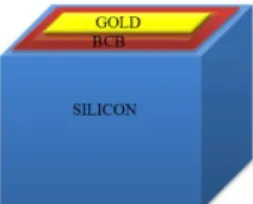
Die-attach module was made using a DBC substrate with gold metal substrate finishes (Cu/Ni/Au). The test vehicles are presented in Figure 5, the diodes has been sintered on the substrate.
Figure 5: test vehicle after silver sintering.
The first assemblies using silver sintering process were realized and a cross-section has been made (Figure 6
)
.Figure 6: Cross-sectional view of the die attach after silver sintering.
Study of cross-sections shows that silver sintered die-attaches are homogeneous with regular thickness all along the joint and no void can be observed. Furthermore, the diode presents none crack around the trenches termination that confirms the trenches do not restrict assembly solutions with pressure and high temperature.
C. Electrical reverse Characteristics of the DT2 after
sintering
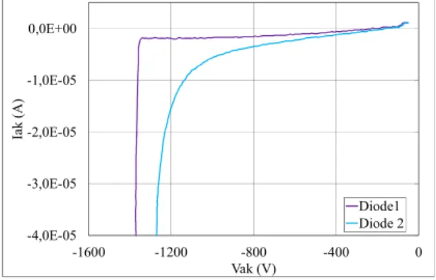
Just after sintering, electrical reverse characteristics were performed with the aim at verifying that the sintering process did not effect on the electrical characteristics, and to confirm that a 4-year storage in clean room did not degrade this electrical parameter. Figure 7 presents the two main behaviors measured. The first is named “Diode 1” with a low leakage current and the second is named “Diode 2” with a higher leakage current.
Figure 7: Measured I-V reverse characteristics after sintering.
The DT2 breakdown voltage keeps a value above 1200V
after sintering. The reverse characteristics are recorded in -4,0E-05 -3,0E-05 -2,0E-05 -1,0E-05 0,0E+00 -1600 -1200 -800 -400 0 Iak (A) Vak (V) Diode1 Diode 2
order to keep it as reference, and to compare with characteristics after thermal ageing.
IV. THERMAL AGEING
During the lifetime a component is exposed to passive temperature swings coming from the environment and active temperature cycles generated by self-heating under operation. Temperature cycling and power cycling tests represent these conditions. Then, to simulate the real application, passive power cycling tests are most commonly used in the qualification procedure for component.
A. Experimental approach
A climatic chamber with two independent rooms has been used. Temperature has been set up to two specific values. In this study, standard temperature profile has been set up: a high temperature value of +125°C and a low temperature of -40°C are fixed as depicted inFigure8.
Figure 8: Thermal ageing profile.
B. Results
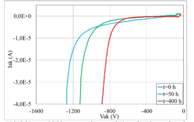
Every 50 thermal cycles, the thermal cycling is stopped and the I-V reverse characteristics were achieved. Figure 9 exhibits the reverse characteristics after thermal ageing for the diodes 1. An increase of the breakdown voltage can be observed for such diodes. The diodes 1 still present excellent behavior after 400 hours thermal cycling with a breakdown voltage near 1600V.
Figure 9: Measured I-V reverse characteristics after thermal ageing for diodes 1.
An assumption on this variation can be proposed: positive electric charges are stored in the Si/BCB interface and create a
virtual P+/N- junction along the trench. However, no
experimental observation has been made.
Figure 10 exhibits the reverse characteristics for the diodes 2. A decrease of the breakdown voltage with a decrease of the leakage current can be observed for such diodes. The diodes 2 still present excellent behavior after 400 hours thermal cycling but with a breakdown voltage near 900V.
Figure 10: Measured I-V reverse characteristics after thermal ageing for diodes 2.
Optical observations do not highlight that a peeling of the resin and silicon can explain these variations. Like for the diodes 1, a hypothesis of this variation is that negative electric charges are stored in the Si/BCB interface, creating a virtual N+/N- junction along the trench. Therefore, finite elements
simulations were carried out.
V. 2D FINITE ELEMENT SIMULATION
In multi-material devices, thermal variations induce a mechanical stress; so it is possible that a separation of materials along the Si/BCB interface and fixed charges appear.
At the Si/BCB interface, more precisely in internal interface of the termination and external interface of the termination, a void with different width has been created to observe its impact on the reverse characteristics (Figure 11).
Figure 11: Void width effect on the reverse characteristic.
The results exhibit that a separation at the interface does not affect the breakdown voltage. This is explained by the fact that the electric field is concentrated at the end of the field plate, like presented in many papers ([1], [7]) and a void insertion does not disturb the electric filed in this region.
-50 -10 30 70 110 150 0 1800 3600 5400 7200 9000 Te mp erat ur e (°C) Time (s) -4,0E-5 -3,0E-5 -2,0E-5 -1,0E-5 0,0E+0 -1600 -1200 -800 -400 0 Ia k ( A ) Vak (V) t=0 h t=50 h t=400 h -4,0E-5 -3,0E-5 -2,0E-5 -1,0E-5 0,0E+0 -1600 -1200 -800 -400 0 Ia k (A ) Vak (V) t=0 h t=50 h t=400 h -8E-07 -6E-07 -4E-07 -2E-07 0E+00 -1600 -1200 -800 -400 0 Iak (A ) Vak (V) Wv=0.1µm Wv=0.5µm Wv=1µm
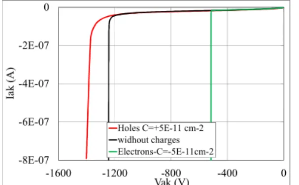
Another type of degradation of the simulated structure is the insertion of fixed charge in the Si/BCB interface. Figure 12 illustrates the I-V reverse characteristics with different Si/BCB interface charges.
Figure 12 : Fixed charges influence at the Si/BCB interface on the reverse characteristics.
The breakdown voltage is modified by charges insertion at the Si/BCB interface. The simulation confirms the device is sensitive to fixed charges and confirms the hypothesis. Nevertheless, the simulation does not explain why the diodes 1 store negatives electric charges and the diodes 2 store positives electric charges.
VI. CONCLUSION
The diodes manufactured 4-years ago have been reported on DBC substrates using silver sintering process. The fear that the trenches terminations cause cracks during sintering has been rule out. This has confirmed that this technology can be integrated in future lead-free packaging. Furthermore, first reliability tests have been achieved. Two behaviors on the breakdown voltage evolution under accelerated ageing are observed. These evolutions can be explained by fixed charges insertion at the Si/BCB interface but more investigations need
to be carried out in order to explain why some diodes store positives charges and other negatives charges.
REFERENCES
[1] L. Théolier, H. Mahfoz-kotb, K. Isoird, and F. Morancho, “A new junction termination using a deep trench filled with benocyclobutene”, IEEE Trans. Electron Devices, vol. A30, pp. 687–689, June 2009. [2] V. A. K. Temple, and W. “ Junction termination extension for the near
ideal breakdown voltage in p-n junction”, IEEE Electron Device Letters, vol ED-33, no. 10, pp.1601–1608, Oct. 1986.
[3] C. B. Goud, K. N. Bhat, “Two-dimensional analysis and design consideration of high-voltage planar junctions equipped with field plate and guard ring”, IEEE Trans. Electron Devices, vol. 38, pp. 1497–1504, Sept. 1991.
[4] D. Jaume, G. Charitat, J.M. Reynès, P. Rossel, “High voltage planar devices using field plate and semi-resistive layers”, IEEE Trans. Electron Devices, vol. 38, pp. 1681–1684, July 1991.
[5] L. Théolier, H. Mahfoz-kotb, K. Isoird, and F. Morancho, “A new junction technique: the Deep Trench Termination (DT2) ,” ISPSD 2009,
pp. 176–179, 2009.
[6] K. Seto, R. Kamibaba, M. Tsukuda, and I. Omura, “Universal trench edge termination design,” ISPSD 2012, pp. 161–164, 2012.
[7] R. Kamibaba, K. Takahama, and I. Omura,“Design of trench termination for High Voltage Device,” ISPSD 2010, pp. 107–110, 2010.
[8] K.O. Lee, Jin Yu, J.Y. Kim, and I.S. Parck, “Thermo-Mechanical Reliability of the Benzocyclebuten (BCB) film in a WLCSP process”, EMAP 2001, pp 84–87, 2001.
[9] A. Tetelin, A. Achen, V. Pouget, C. Pellet, M. Töpper, and J.L. Lachaud, “Water solubility and diffusivity in BCB resins used in microelectronics packaging and sensor applications,” IMTC 2005, pp. 792–796, 2005.
[10] A.Masson, C. Buttay, H. Morel, C. Raynaud, S. Hascoet, and L. Greamillard,“High-temerature die attaches for SiC power devices,” EPE 2011.
[11] F. Le Henaff, S. Azzopardi, J.Y. Deletage, E. Woirgard, S. Bontemps, and J. Jouget, “A preliminary study on the thermal and mechanical performances of sintered nano-scale silver die-attach technology depending on the substrate metallization”, Microelectronics Relability 2012, vol. 52, pp. 2321–2325. -8E-07 -6E-07 -4E-07 -2E-07 0 -1600 -1200 -800 -400 0 Ia k ( A ) Vak (V) Holes C=+5E-11 cm-2 widhout charges Electrons-C=-5E-11cm-2