Control System Implementation for Grating-Element
Positioning and Modulation of the Polychromator
by
Michael Hopgood
submitted to the Department of Electrical Engineering and Computer Science
in partial fulfillment of the requirements for the degrees of
Bachelor of Science in Electrical Science and Engineering
and Master of Engineering in Electrical Engineering and Computer Science
at the Massachusetts
Institute of Technology
May 22,1998
[T .'. 1"1'-<'/")
...J .J ..--~ ~-~.- \. I ....k.,r.l.
@
1998 Massachusetts
Institute of Technology
All rights reserved.
II
I 12
Signature of Author ..
D~p.~~~t
~f"Ei2;~{~~k
2...~...
~t~~.
s~i~~~~
May 22,1998
Certified by
S.t~ph~~
n&~.~gci~i~~.;~~
Department of Electrical Engineering and Computer Science
esis Supervisor
~~, /
Accepted
~y _._. ,. _..
. _..
... __'_.~
.
J(~ __.. __. ~~ -:-. . ....Arthur
. Smith
Chairman, Committee on Graduate Students
Control System Implementation for Grating-Element Positioning and Modulation of the Polychromator
by
Michael Hopgood submitted to the
Department of Electrical Engineering and Computer Science May 22,1998
In partial fulfillment of the requirements for the degrees of Bachelor of Science in Electrical Science and Engineering
and Master of Engineering in Electrical Engineering and Computer Science Abstract
The Polychromator is a MEMS-based optical diffraction grating with a large number of individually controllable micromirror grating elements which can be electrically
programmed to reproduce spectral features of many target chemical species. This thesis reports on the implementation of the control system used to actuate the polychromator. The polychromator design and the test electronics used are described in detail. A model to simulate the actuation of a grating-element is developed in order to obtain a voltage-displacement relationship. The implementation for static displacement and modulation are discussed. The problems encountered, future work possibilities, and the conclusions are presented.
Thesis Supervisor: Stephen Senturia Title: Barton L. Weller Professor,
Acknowledgments
I would like to take this opportunity to thank the many individuals who have contributed to my personal and academic growth culminating in the completion of this thesis.
Most important in this work is the expert guidance of my research and academic advisor Stephen Senturia. Steve was responsible for introducing to the Polychromator project and getting me interested in joining the group. His support and guidance have been crucial throughout my stay at MIT.
The members of my research group have been instrumental both technically and socially in making this work a success. In particular, Elmer Hung and Erik Deutsch have been insightful and helpful in many ways throughout this project. I would also like to thanks the members of the Polychromator team at Sandia National Laboraties and Honeywell Technology Center who given me their support and appreciation.
Finally, I would like to thank my parents Ronald and Rosa, my brother Ronald, my sisters Maria T. and Margarita, and my entire family for their never ending love, support, and guidance throughout my life, especially my time here. They have made my success in life a reality.
Research was done in the Technology Research Laboratory and the Senturia group research facilities at the Microsystems Technology Laboratory, and at the Center for Materials Science and Engineering.
The Polychromator project is a joint effort between the Honeywell Technology Center, Sandia National Laboratories, and the Massachusetts Institute of Technology and supported by Defense Advanced Research Projects Agency under contract N66001-97-C-8620.
This work made use ofMRSEC Shared Facilities supported by the National Science Foundation under Award Number DMR-9400334.
Table of Contents
CHAPTER 1. INTRO D U CTI 0 N 7
1.1 THESIS OlJfLINE 7
1.2 MOTIVATION 7
1.3 PROBLEM STATEMENT 8
CHAPTE R 2. BACK G ROUND 9
2.0 OVERVIEW 9
2.1 POL YCHROMATOR 9
2.1.0 Overvielv 9
2.1.1 Concept 9
2.1.2 Actuation 11
2.1.3 Layout and Interface 12
2. 2 ANALOG DRIVER 12
2.2.0 OvenJielv 12
2.2.1 Description 13
2.2.2 Operation 14
2.2.3 Interface 15
CHAPTER 3. SIMULATIONS AND DESIGN 16
3.0 OVERVIEW 16 3.1 INTERFACE 16 3.1.0 Overvielv 16 3.1.1 Grating-element mapping 16 3.1.2 Results 17 3.2 SIMULATION 17 3.2.0 OvenJielv 17 3.2.1 Polychromator I1lodel 18 3.2.2 Voltage-Displacement Relationship 19
3.2.3 Results 19 3.2.4 Calibration 20 3.3 POSITIONING 20 3.3.0 Overview , 20 3.3.1 Static displacement 20 3.3.2 Implementation , 21 3.4 MODULATION 22 3.4.0 Overview 22 3.4.1 Strategies 22 3.4.2 Implementation 23 3.4.3 Results 24
CHAPTER 4. DISCUSSIO N AND CON CL USIO NS 25
4.0 OVERVIEW 25 4.1 PROBLEMS , , 25 4.1.1 Shorting , 25 4.1.2 Crosstalk 26 4.2 FlJ1lJRE WORK , 27 4.3 CONCLUSIONS 28 REFE RE NCES: 29
APPE NDIX A: FIGURE S 30
APPENDIX B: TEST EQ UIPMENT 37
APPENDIX C: CHIP TEST MODULE CHANNEL MAP 38
APPENDIX D: SAMPLE VOLTAGE-DISPLACEMENT FILE 39
APPENDIX E: SAMPLE MODULATION FILE 40
Table of Figures
FIGURE 1. COMPARISON BETWEEN TRADITIONAL CORRELATION SPECTROSCOPY USING A REFERENCE CELL TO ANALYZE MATERIAL AND HOLOGRAPHIC CORRELATION SPECTROSCOPY USING A MEMS-DEVICE AS A
PROGRA.i.\fMABLEOPTICAL FILTER 8
FIGURE 2. CROSS SECTION OF THE POL YCHROMATOR SHOWING DEFLECTED MICROMIRROR ELEMENTS AND DRIVER ELECTRODES. THE OUTPUT POLYCHROMATIC SPECTRUM CAN BE DESIGNED TO REPRODUCE THAT
OF A SPECIES OF INTEREST, HFIN THIS EXA\1PLE [3] 10
FIGURE 3. BASIC GRATING ELEMENT DESIGN SHOWING TWO-LEVEL STRUCTURE. THE LOWER STRUCTURAL LAYER (POLY2) IS DEFLECTED BY ELECTROSTATIC FORCES THROUGH LEVERAGED BENDING, WHILE THE UPPER (poLY3) LAYER WITH THE MIRROR SURFACE REMAINS FLAT [3]. 11 FIGlJRE 4. CONTROL ELECTRONICS SETUP USED TO DRIVE THE POLYCHROMATOR (POLYC) 13 FIGURE 5. SCHEMATIC REPRESENTATION OF THE INTERNAL INTERFACE OF THE HV ADI HARDWARE
DESCRIBING HOW THE INFORMATION PASSES FROM THE COMPUTER TO THE OUTPUT STAGE 14 FIGURE 6. BASIC GRATING ELEMENT DESIG~ SHOWING TWO-LEVEL STRUCTURE AT REST (NO VOLTAGE
APPLIED BETWEEN POLY 1 A."\!DPOLY2) 30
FIGURE 7. LARGE GRATING AT THE WAFER-LEVEL. 30
FIGURE 8. LARGE GRATING IN 145-PIN PGA PACKAGE 31
FIGURE 9.FRONT VIEW OF THE HIGH VOLTAGE ANALOG DRIVER INSTRlJMENT (HVADI) 31 FIGURE 10. BACK \lEW OF THE HV AD!. SHOWING CONNECTIONS FOR THE 4 RIBBON CABLES A'1D THE
P..\RA.LLEL PORT 32
FIGURE 11. Cl-IIP TEST MODlTLE 32
FIGURE 12. CHIP TEST MODULE WITH THE POLYCHROMATOR INSERTED 33
FIGURE 13. VOLTAGE SIGNATURE FOR HVADI CHA1,\;NEL75. NOTE THAT HIGH IS EQUAL TO 150 VOLTS, LOW IS EQUAL TO 50 VOLTS AND THE STARTING MARK IS EQUAL TO 25 33 FIGURE 14. OUTPur VOLTAGE WAVEFORMS FOR A FIRST DERIVATIVE SCHEME (TWO STATES) 34 FIGURE 15. OlJTPUr VOLTAGE WAVEFORMS FOR A SECOND DERIVATIVE SCHEt\m (THREE STATES) 34 FIGURE 16. OUTPur VOLTAGE WAVEFORMS FOR "FOLLOW THE LEADER" STATE SWITCHING. NOTE THAT
CHAI\"NEL 2 IS OFFSET FROM THE X-A.'XISIN ORDER TO OBSERVE BOTH CHfu"'\TNELSSIMULTA'l'EOUSLY 35 FIGURE 17. CROSS SECTION OF TWO GRATING ELE~tENTS AITER DEPOSITION OF POLY2 35 FIGURE 18. CROSS SECTION OF TWO GRATING ELEME~TS RIGHT AITER POL Y2 IS PATfERNED 36
Chapter 1. Introduction
1.1 Thesis Outline
The goals of this work are presented by the way of the thesis outline. This chapter along with providing the motivation for this project, discusses the method chosen to control and actuate the polychromator in order to produce the desired behavior.
Chapter 2 begins with a description of the polychromator, and the test electronics chosen to drive the polychromator chip. In Chapter 3, we first discuss how the
polychromator and the electronics interface with each other. Second, we develop the simulation model for the grating-element actuation and create a voltage-displacement
relationship. Finally, we discuss how the static displacement and modulation strategies are implemented. Chapter 4 contains a discussion of some of the problem areas found while performing tests on the grating-elements. It also outlines future areas of investigation in order to achieve better understanding of the polychromator actuation. Finally, a summary of all the work done is presented.
1.2 Motivation
Traditional correlation spectroscopy requires the use of a reference cell in order to analyze a sample material. The process of using the reference cell can be cumbersome since we need to replace the cell every time we want to look for a new material in our sample. Also if we are looking for labile species, the handling of the reference cell becomes a very important issue. Instead, we can use a form of holographic correlation spectroscopy to use the benefits of correlation spectroscopy but obtain much greater
Source Source Sample Cell Sample Cell Reference Cell Diffractive Element Filter Detector
t
Detectort
Traditional Correlation Spectroscopy Approach Holographic Correlation SpectrometerFigure 1. Comparison between traditional correlation spectroscopy using a reference cell to
analyze material and holographic correlation spectroscopy using a MEMS-device as a programmable optical filter.
We replace our reference cell with a MEMS-based diftTactive element, called the polychromator, which allows us to control its optical characteristic by electrostatic
actuation. The diffractive element reduces the overall size of the spectrometer system and eliminates the need for a reference cell. This method leads to the development of a
miniature, electronically programmable remote chemical detection system for field use.
1.3 Problem Statement
The problem addressed in this thesis is to create the control program for the analog driver to permit static displacement and modulation of each grating-element, demonstrate the system with interferometric profilometry, and verify the robustness of the system by comparing the repeatability and accuracy from element to element and die to die.
Chapter 2. Background
2.0 Overview
This section describes the polychromator concept and how the actuation of each grating-element is achieved. Also, the operation of the test electronics used to drive the polychromator is explained.
2.1 Polychromator
2.1.0 Overview
The Polychromator is a MEMS-based optical diffraction grating with a large number of individually controllable micromirror grating-elements which can be electrically programmed to reproduce spectral features of many target chemical species[I,2]. The synthetic spectra and the displacement profile producing such spectra can be computer generated in advance. This allows for a very easy and flexible programmable system.
2.1.1 Concept
Correlation spectroscopy has advantages for chemical sensing and analysis because of its mechanical and optical simplicity, and its high selectivity [1]. In correlation
spectroscopy, the cross-correlation of the spectra of a reference cell containing a target compound and that of an unknown is obtained over a range containing multiple spectral lines.
This new MEMS device consists of a linear array of perhaps several thousand elastically supported micromirror grating-elements, with the displacement of each element independently controlled by electrostatic actuation. This device is called a polychromator grating, and is shown schematically in Figures 2 and 6 [I, 2]. When illuminated with broad-band white light, the polychromator can be programmed and electrically controlled to produce a spectrum containing selected lines, or reproduce spectral features of any target molecule or combination of molecules.
Deflectable Mlcromirror Grating
Elements
---~
Indivu:lualy Addressable Array of Dnver Electrodes
Broadband Ughlln
---:::.:.:.::~~::.~..~- ~" .;0: '<''''' ... __ :lr_ J. _ - + 0.00 I 3600 3700 3800 3900 4000 4100 4200 wavenumbers (c~
Figure 2. Cross section of the Polychromator showing deflected micromirror elements and
driver electrodes. The output polychromatic spectrum can be designed to reproduce that of a species of interest. HF in this example [3].
The advantages of combining correlation spectroscopy with the polychromator provide the breakthrough capability of electronic programmability, while eliminating the troublesome reference cell. This permits one system to rapidly search for many species, including examination of labile species, such as reaction intermediates, highly corrosive species, and acutely toxic substances.
2.1.2 Actuation
The Polychromator depends on accurate positioning and modulation of each micromirror grating element in order to produce the desired synthetic spectrum. The grating-element actuation method chosen is a combination of electrode and mirror-element design called "leveraged-bending", shown in Figure 3 [7]. Electrodes are placed beneath only about 1/3 of the element, specifically positioned towards the supports. As long as the element itself is bending dominated rather than stress dominated (requiring stress below about 10 MPa in our baseline case), then the bending produced by electrostatic actuation near the supports is leveraged into full travel of the center of the element, without
encountering pull-in. Mirror surface Landing electrodes (Grounded) -500Jlm
Si Substrate
Grating elements tiled lengthwise ~ •••
(Each mirror extends - lcrn in length)
Figure 3. Basic grating element design showing two-level structure. The lower structural layer (Poly2) is deflected by electrostatic forces through leveraged bending, while the upper (poly3) layer with the mirror surface remains flat [3].
Modeling of the grating-element voltage-displacement characteristics provides a first-order calibration of mirror movement, to support both grating positioning and modulation. Models of grating-elements are already done but full calibration of the calculated characteristics awaits experimental confirmation from the first test parts. The
characteristics of the grating-elements are experimentally calculated using the MIT
developed in-situ material test procedure (M -Test), a method for measuring residual stress and elastic modulus of thin-film structures [4, 5].
2.1.3 Layout and Interface
The polychromator contains 128 controllable elements each requiring high voltages in order for Poly2 to travel down the whole gap between Poly2 and the grounding pad. The actual gratings contain 640-1024 total lines arranged in groups of
128 (Figure 7). In order to apply a voltage to each of the grating-elements, the grating array die is packaged on a 145-pin PGA (Figure 8), and connected by 132 bond pads (128 actuation voltages
+
4 ground pads). See Appendix F for package information.2.2 Analog Driver
2.2.0 Overview
The electronic programmability of the polychromator requires the development of a control system in order to operate and control the behavior of each grating-element. The control electronics is composed of two main pieces of hardware: a high voltage analog driver instrument (HV ADI) and a personal computer (Figure 4).
Control Electronics
• I 28-channel (Digital Designs & Systems) analog driver - controlled by computer • Dell PentiumII-300 MHz PC
...
Bi -directional Parallel Port 4 ribbon cables40-pins wide • ZIF Socket
Figure 4. Control electronics setup used to drive the polychromator (PolyC).
The test electronics (Figure 9) is composed of a 128-channel programmable high voltage analog driver (being purchased from Digital Designs & Systems), with a range of
o
to 150 V, a 32-word frame buffer for each channel (permitting modulation up to 1 kHz), and a voltage feedback to permit device monitoring.2.2.1 Description
The purpose of the test electronics is to supply a high voltage capability and a frame buffer that allows sets of voltages to be stored in memory. The hardware is controlled by its own DSP processor that communicates with the PC through the parallel port. The PC passes the instructions to the DSP, gives the desired output voltages, and reads the actual output voltages.
direct output mode (frame buffer bypass)
i
4-ribbon cables 40-pins wide outputrefresh
*
output read (controlled by DSP)
HV ADI Interface
o
!
Bi -directional Parallel Port*
The output refresh operation is controlled by a trigger event, either internal (DSP) or ex1:ernal (source input).Figu re 5. Schematic representation of the internal interface of the HV AD I hardware describing how the information passes from the computer to the output stage.
2.2.2 Operation
The instrument has several modes of operation: single frame mode, loop frame mode, continuous frame mode, and direct output mode. In the single frame mode, only one frame is used to control the output voltage (requires the PC to send a new frame in order to update the output). In the loop frame mode, a series offrames are passed to the buffer and the HV ADI cycles through the frames until it is interrupted (no information required from PC once all frames in cycle are in the buffer). The continuous frame mode requires the PC to continuously send frames to the buffer in order to update the output (the information in the buffer is stored as fast as the PC can send it). An update will only occur when the buffers receive a new frame. Finally, the direct output mode bypasses the
buffer completely passing the desired voltages directly to the output. In this mode there is no update and the buffer is not used.
The speed of the output update is controlled by the trigger source which can be set to be either internal or external, but not both at the same time. Internally, the function HV ADI_SetFrequency(Hertz) controls the frequency of the updates. Externally, the updates are controlled by using a series of pulses, each pulse triggering one update event.
2.2.3 Interface
The HV ADI hardware interfaces with two parts: the PC and the Chip Test Module (see Figure 10). The computer is connected through a bi-directional parallel cable and the Chip Test Module (Figure 11) through 4 ribbon-cables, each 40-pins wide. The correct interface between the polychromator and the Chip Test Module is to be determined and documented (see Section 3.1).
Chapter 3. Simulations and Design
3.0 Overview
This section outlines the procedures taken to produce the grating-element voltage-displacement characteristics, the grating-element positioning strategy, and the modulation strategies chosen to produce spectral modulation.
3.1 Interface
3.1.0 Overview
One of the most simple but easily overlooked problems is the interface between any two systems. If the communication between the systems is not mapped correctly, the overall system will not work correctly even if the control strategies are accurate.
Therefore, it is necessary to verify that the analog driver and the polychromator "speak the same language".
3.1.1 Grating-element mapping
The polychromator grating, as described previously, is packaged using a 145-pin PGA chip to provide a rigid connection to the control electronics. This chip is inserted into the chip test module of the HV ADI hardware (Figure 12), gold strip in the package points away from the jumpers in the module. There are two steps required to verify the proper interface. The first is the channel map of the HV ADI to the chip test module and the second is the layout map of the PGA package, the pins in the back to the
In order to map the chip test module, an identifying signature was produced for every channel and then that signature was located in the module. The signature corresponds to the base 2 representation of the channel number, i.e. signature 1001011 for channel 75 (Figure 13). Note that the channel number for the HV ADI run from 0 to 127, therefore channel 0 corresponds to grating-element # 1. The package layout was provided by Honeywell and the grating layout by E. S. Hung.
3.1.2 Results
A table map was created using the identification of the signatures in the chip test module (Appendix C). This table was then compared to the package layout, and
subsequently, to the bond pad connections of the polychromator grating. The interface connections were verified and only one error was identified. A bond pad connection had been misplaced which shifted the HV ADI channel- grating-element mapping. The error was corrected for future packaging of grating arrays.
3.2 Simulation
3.2.0 Overview
Accurate and efficient models are necessary to produce a repeatable and accurate actuation behavior. Modeling of the grating-element voltage-displacement characteristics provides a first-order calibration of mirror movement, to support both grating positioning and modulation.
3.2.1 Polychromator model
For our model, we follow the example set forth by E. S. Hung and S. D. Senturia [7]. Since the upper mirror beam does not affect actuation to first order, the grating element is modeled by considering just the lower beam. The 2D equilibrium equation for an elastic beam with the electrostatic force is given by:
~z
ffz
EI--S(z)-=F
~4 ~2 eke (1)
where x is the distance along the beam, z(x) is the gap height, E is the elastic modulus,
I
=
wh3/12 is the moment of inertia, w is the beam width, h is the beam thickness, S(z) is the force in the beam due to stress (see Eq. (3», and
F:zee
is the electrostatic force per unit length. Neglecting fringing fields and crosstalk between elements, we approximate:.,
F = __&o_a_(x_)_V_-elec 2X2 (2)
where a(x) represents the shape of the actuation electrode, and
Vis
the applied voltage. The S(z) terms contains two contributions, one from the residual stress left in the beam after processing, and one from a nonlinear "strain-stiffening" effect due to the streching of the beam as it deforms. S(z) is modeled as follows:M
S(z) =hw[ao(l- v)
+
EL
]
(3)where
a °
is the biaxial residual stress,v
is the Poisson ratio, M is the elongation in the length of the beam due to deformation, andL
is the length of the beam. The beam equation is simulated using finite difference code.3.2.2 Voltage-Displacement Relationship
In order to actuate the polychromator grating, we need to obtain a translation table between grating-element displacement and voltage. This relationship allows conversion of a specific displacement profile into the corresponding voltage profile that will produce the desired behavior.
The model used for the polychromator obtains the grating-element displacement that corresponds to a specific electrostatic voltage applied to the electrode. A reverse lookup procedure is used to iterate over the simulation and find the electrostatic voltage that corresponds to a specific displacement. Two translation tables were produced: one with 16 discrete positions for DC positioning and another with displacement in steps of 0.0 1IJ.mfor more refined positioning and accurate modulation.
3.2.3 Results
The results of our reverse lookup calculations are stored in an output text file [Appendix D]. The translation file contains the parameters used to produce the file, a brief description of its contents, and the translation table. The table is composed of two
columns: the first is the displacement in IJ.m,and the second is the required voltage. The displacement column corresponds to the distance away from the relaxed position instead of the gap distance. This allows the polychromator grating to be modified without having to change the interpreting software.
3.2.4 Calibration
Models of grating-element displacement versus voltage were obtained to a first degree, but full calibration of the calculated characteristics awaits experimental
confirmation from the first test parts. The characteristics of the grating elements are experimentally calculated with the use of the M- Test procedure [4, 5].
There are two effects that were not modeled using our finite-difference code that could produce significant changes in element behavior. First, crosstalk between grating-elements can produce a more complex actuation behavior since the displacement of a specific grating-element would depend on the adjacent grating-elements. Second, more complex models that take into account support compliance, exact geometry, and extracted material properties should be used in order to produce more accurate characteristics.
3.3 Positioning
3.3.0 Overview
In order to observe the desired actuation displacement, the control system for the polychromator must be able to convert a specific displacement profile into a
corresponding voltage profile that will produce the desired displacement. The translation process requires accurate grating-element to voltage-displacement characteristics to produce repeatable and accurate actuation of the polychromator.
3.3.1 Static displacement
F or the simplest model, we assume that all channels observe the same voltage-displacement relationship. In this case, all that is required is to take a specific
displacement profile, convert it into a voltage profile which in turn is passed to the HV ADI hardware, and then actuates the polychromator. Ifit turns out that not all the grating-elements observe the same relationship, we can use several relationships at the same time and reference each element accordingly when the conversion is desired.
3.3.2 Implementation
The conversion process from displacement to voltage is done by means of a table lookup (see Appendix D). One of the main reasons for using a text file to hold the voltage-displacement relationship is that we can either create the file from a simulation or enter the data from actual measurements. In the case that a specific displacement is not found in our table, an interpolation is done using the closest values in the table by giving more weight to the higher displacement (the electrostatic force is directly related to the square of the applied voltage). In order to test the conversion from displacement to voltage, we can use the modulation implementation with only one state (see next section for details).
In order to calibrate and test static displacement on individual or groups of grating-elements, we can use a program developed in conjunction with E. S. Hung that allows the user to apply DC voltages to the grating-elements in four different modes: same voltage to all channels, voltage to a specified channel, voltage to odd-numbered channels, and voltages to even-numbered channels (channels not specified receive 0 volts). There is also a fifth mode under consideration in order to enter displacements profiles by adding the functionality of the modulation scheme (see next section). The legend
HVADI support library Version 1.01. [Apr 5 199821:44:34] DC Grating Testing (Interactive Single Frame Mode) Press the following keys at any time:
Channel selection:
m: Select all channels (default) c:Select output channel (0-127) o:Select odd channels.
e:Select even channels. Voltage manipulation:
z:output voltage -I V, x:voltage +1V a:output voltage -IOV, s:voltage +10V Measure all channels:
p:Print ADC values
r:Print resitance values (in MOhm) q:Terminate program
?:Print this menu
In the case where more than one voltage-displacement relationship exist, we can add more columns to our lookup table file (see Appendix D) and then use another table to map each channel to the corresponding relationship.
3.4 Modulation
3.4.0 Overview
The polychromator spectrometer system uses a correlation detection scheme in order to determine the presence of a target species. To use this detection scheme, we need to implement a modulation behavior that shifts the target spectra and produce a high-selectivity only of the species in study.
3.4.1 Strategies
The modulation strategy that was chosen uses a first-derivative detection scheme proposed by Mike Sinclair (Sandia). This method uses a two state-switching modulation
scheme where two output target spectra are used for a specific target species and the difference in the output signal is used to determine the presence of the species. In addition, a second-derivative detection scheme (three states) was proposed by S. D. Senturia which might give even better results. It is possible that with our current design we don't have enough actuation lines to take full advantage of this method and that will need to be determined.
3.4.2 Implementation
In order to allow the most flexibility to the system, both derivative schemes were implemented. The information required by the control system, namely the different
displacement profiles that compose the required derivative scheme, was implemented as a text file to keep the inputs and the control program separate.
The text file contains a brief description of its function and a table with the corresponding states for the derivative scheme (Appendix E). In order to distinguish between the first-derivative and second-derivative scheme, the input file requires the following identifying line "%n" where n is the number of states (n=2 for first-derivative, n=4 for second-derivative). The columns in the file are mirror #, state al and state a2for first-derivative, followed by state al and state a3 for second derivative.
The control system reads all the states from the input file and keeps it in memory until another input file is desired, or the system is exited. The program translates each displacement state profile into a voltage profile and passes it to the frame-buffer in the HVADI.
3.4.3 Results
The results of the modulation scheme are very promising and allow great flexibility in the programming of the control system. Two output modulations are shown in Figures
14 and 15. This modulation method allows many different patterns to be used to test the grating. An example with two grating-elements is shown in Figure 16. We apply a "follow the leader" state switching where both lines start at the same position
and only one line changes at a time. Line 1 and 2 start at PI, Line2 changes to P2, Line 1 changes to P2, Line2 changes to PI and the cycle repeats. If we observe this test under an interference microscope, we can determine ifboth channels have the same
voltage-displacement relationship by comparing the number of fringes when both channels have the same applied voltage.
Chapter 4. Discussion and Conclusions
4.0 Overview
This section discusses some of the problems encountered with grating-element actuation, and presents possible explanations and areas of further study to eliminate the problems. It is followed by a discussion of suggested areas of investigation that will provide a better understanding of the grating-element actuation and a more accurate control of the polychromator. The chapter concludes with a summary of the work done for this thesis.
4. 1
Problems4.1.1 Shorting
In many of the beams that were tested, there was a "shorting" behavior that did not allow the grating-elements to travel the full gap. Initially, these gratings would deflect downwards as expected with increasing voltage. As the applied voltage reached around 40-50 volts (in most cases), the resistance between the actuation and ground pads
suddenly dropped by a factor of 10 or more. Most of the voltage drop occurred between the interconnects and the test resistor (used to measure current drawn), effectively reducing the voltage between the actuation electrode and the rest of the grating. This "shorting" behavior caused the grating-element to pop back up to an undetlected position.
A lot of testing was done in order to determine the cause of the "shorting"
behavior. With some destructive testing, E. S. Hung was able to identify the mechanism behind this strange behavior. The layout of the layers below Poly2 cause a ditch to be
formed between grating-element which causes a larger height of Poly2 in this area during its deposition (Figure 17). When Poly2 is patterned and etched, the extra height causes a small stringer to be left behind that will cause a great deal of problems during the actuation of the gratings (Figure 18).
These stringers act like small cantilevers connected to the Poly2 structure. When a voltage is applied to the electrode, these cantilevers bend towards the electrode. At the moment where the stringer comes in contact with the actuation electrode, a "shorting" behavior is exhibited since the Poly2 structure is now at the same potential as the electrode and the grating returns to an undeflected position. In some cases, the stringer becomes permanently stuck to the electrode, and prevents using that particular grating-element. In order to eliminate the presence of these stringers, longer etch times are being used during the manufacturing process.
4.1.2 Crosstalk
Another behavior that was noticed during the actuation of some gratings was a considerable crosstalk effect between grating-elements. As voltage was applied to one line, the line next to it deflects partially. Even if the electrode of the next line was
grounded, there was still some crosstalk between the elements. In our simulation model, we assumed that adjacent elements did not affect each other but it may turn out that our assumption was wrong.
There are a few reasons that might be causing this crosstalk effect. First, our infamous stringers which may cause undesired connections between adjacent elements. Second, a leakage current through the nitride layer which may cause a voltage in the
adjacent electrode or ground pad. Finally, a fringing field between the actuation electrode and the adjacent grating-elements could cause undesired effects.
4.2 Future Work
There are a four main areas of investigation that will lead to a better understanding of the grating-element actuation and a more accurate control system for the
polychromator. First, obtaining a more accurate simulation model of the polychromator is necessary in order to produce a more accurate voltage-displacement relationship. The first step in obtaining a better model is to calibrate the characteristics of the grating-elements using the M- Test procedure [4,5]. Another step is to use a more complex model that takes into account the presence of the adjacent grating-elements in order to
understand the effect of the neighboring electrostatic forces. This step is very important since we noticed considerable crosstalk effects between the elements, and the source could not be easily identified.
Second, exhaustive interferometric measurements using both the WYKO optical profilometer an the interference microscope (fringe counting) are needed in order to assess the accuracy of our model and get a more specific voltage-displacement relationship. Third, it is important to understand the dynamic response of the grating-elements in order to determine how the elements will react to changes in the actuation voltage. The natural mechanical frequency can cause ringing effects of the grating-element position which will produce disturbances in the output spectra. Finally, it is necessary to verify the
repeatability and accuracy of each grating-element. It is important to determine if different grating-elements exhibit different voltage-displacement relationships in order to calibrate
the voltage-displacement table. It is also important to determine if there is any charge accumulation in the grounding electrode or if there is any leakage current through the nitride layer which will cause time-dependent electrostatic forces.
The continuing investigation of these areas is vital to assure that the polychromator exhibits a predictable and accurate actuation behavior. This characterization will ensure that the optical performance of the device will be consistent and that no calibration would be required for each manufactured device.
4.3 Conclusions
The control system implementation for the polychromator is presented. The static displacement and modulation strategies were designed to be as modular as possible using input files to address all the information required: voltage-displacement relationship and displacement profiles. This allows us to modify our design without having to make changes to our implementation and reproduce our input files with simulated or measured values. The control system implemented will make it very easy to integrate the detection and analysis system that is being developed at Sandia National Laboratories.
As part of this thesis, areas of further study are identified wherever possible in order to achieve better understanding of the grating-elements actuation and the accurate control of the system in order to produce accurate spectral features. The polychromator concept will considerably change the way chemical detection is performed at present, both as a spectrometer system and as remote sensing equipment for field use. The control system implemented will provide the tools necessary for the actuation of the
References:
[1]
"Synthetic spectra: A Tool for Correlation Spectroscopy," M.B. Sinclair, M.A.
Butler, A.J. Ricco, and S.D. Senturia, Applied Optics 36, pg. 3342-3348 (May 20,
1997)
[2]
"Synthetic Infrared Spectra," M.B. Sinclair, M.A. Butler, S.H. Kravitz, W.J.
Zubrzycki, and A.J. Ricco, Optics Letters 22, pg.1036-1038 (July 1,1997)
[3]
G. B. Hocker, et. aI., Polychromator Semiannual Report, Contract Number
N66001-97-C-8620, January 1998.
[4]
P. M. Osterberg, and S. D. Senturia, "M-Test: a Test Chip for MEMS Material
Property Measurements Using Electrostatically Actuated Test Structures", Journal
of Microelectromechanical Systems, June 1997, Vol. 6, No.2, pp. 107-118.
[5]
Raj K. Gupta, "Electrostatic Pull-In Test Structure Design for in-situ Mechanical
Property Measurements of Micro electromechanical Systems (MEMS)", Ph.D.,
June 1997, MIT.
[6]
Elmer S. Hung, "Positioning, control, and dynamics of electrostatic actuators for
use in optical and RF systems", Ph.D., August 1998, MIT.
[7]
"Leverage Bending for Full-Gap Positioning with Electrostatic Actuation," Elmer
S. Hung, and S. D. Senturia, to be presented.
Appendix A: Figures
Metal Poly3 Poly2
Figure 6. Basic grating element design showing two-level structure at rest (no voltage applied between
Poly 1 and Poly2).
Figure 8. Large grating in 145-pin PGA package.
Figure 10. Back view of the HV ADI, showing connections for the 4 ribbon cables and the parallel port.
Figure 12. Chip Test Module with the Polychromator inserted.
Tek Run: 2. 50kS/s[-.:r.~~~~~.~ . ._. .. +_~rig_ler Position: 5%
67Hz' Trigger @ 7 Hz Position
...
~ .. ~ .I---t Set to 10%:t
.~.;--+..+..+-i++-+i ..+...j-'+'-i-'+'+-+"';''''i-+-+-+-;+++''''~'-++";"'+"++';"-1-++-+-;-++...
t
::
-;-++-;--~-+-+--i-~.
t : I . I i .[ . t I .. i50.0 V i ~ Set to 50% ~ Set to 90%
Figure 13. Voltage signature for HVADI channel 75. Note that high is equal to 150 volts, low is equal to 50 volts and the starting mark is equal to 25.
Tek Run: 2.50kS/s Sample
~-~---~
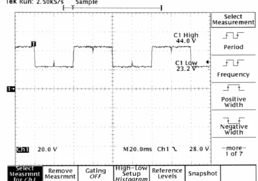
Select . Measurement C'.High" 44.0 V Period Frequency Sill ..20:0 \i Positive Width L--1 Negative WidthFigure 14.Output voltage waveforms for a first derivative scheme (two states).
Tek Run: 2.50k.S/s Sample
[-T---j
ACrv
GNDih
.20:0 \i
Tek Run: 2.50kS/s Sample (--.T- ....--.--.--.- ...- ..-- ..-...-...-.-- ..- ...---] Remove : Measurement : Measurement 1 . Measurement 2 .... -~_++-+-!-+++.+-+-i-!-+.+-~1.-!_+_!-;.-4-+-+-+._~+.+-;- ..t--~.-+--t-t-;.-~_...-!-++-+~: -: !-+-H-+-!-. Measurement . 3 : Measurement ... -- 4 20.0 V 28.0 \;. All . Measurements
Figure 16. Output voltage waveforms for "follow the leader" state switching. Note that channel 2 is offset from the x-axis in order to observe both channels simultaneously.
Actuation
electrode
Space between
grating elements
Poly2 stringer beam
Actuation
electrode
High voltage
electrode
Space between
grating elements
Appendix B: Test equipment
The following is a list of the test equipment used to perform the research described in this thesis.
1. 128-channel (Digital Designs & Systems) analog driver instrument 2. Dell PentiumII-300MHz PC
3. Tencor P-I0 Surface Profilometer 4. WYKO Optical Profilometer 5. Interference Microscope 6. Tektronix TDS 540B
Appendix C: Chip Test Module channel map
The following table showing the HV ADI channel mapping on the Chip Test Module where the polychromator package is inserted.
Channel map for HVADI Chip Test Module (handle on right)
ABC
0
E
F
G
H
JK
L
M
N
P
R
GND 93 89 88 86 82 81 78 76 75 72 69 67 64 GND 96 GND 92 90 87 84 83 77 73 71 68 65 GND GND 61 99 GND 95 94 91 85 80 79 74 70 66 GND 63 60 57 101 97 GNDI
I I I I I I I 62 62 58 56 104 100 98 I I I I I I I I 59 59 55 54 107 103 102 II
I I II
II
I 53 52 50 108 105 106I
I I I I I I I I 48 51 49 110 109 111 II
I
II
II
II
47 45 46 113 115 112I
I I I I I I I I 42 41 44 114 116 117 I I I II
I I I I 38 39 43 118 119 123I
I I I I I I I I 34 36 40 120 122 126 II
II
I
I
I
II
GND 33 37 121 124 127 GND 2 6 10 15 16 21 27 30 31 GND 35 125 GND GND 1 4 7 9 13 19 20 23 26 28 GND 32 GND 0 3 5 8 11 12 14 17 18 22 24 25 29 GND 15 14 13 12 11 10 9 87
6 5 4 3 2 1Appendix D: Sample voltage-displacement
file
This is sample input file used to describe the voltage-displacement relationship. The lines starting with
*
are used to describe the function of the file. The columns in the table are the displacement in J.lmand its corresponding actuation voltage.*
Polychromator displacement vs. voltage profile*
for 16 preset positions*
Displacement Voltage 0.0 0.0 0.125 19.0754 0.25 26.9818 0.375 33.3068 0.5 39.0139 0.625 44.4648 0.75 49.7988 0.875 55.0771 1.0 60.2886 1.125 65.3999 1.25 70.3553 1.375 75.0656 1.5 79.442 1.625 83.384 1.75 86.7609 1.875 89.4307Appendix E: Sample modulation file
This is sample input file used to describe the modulation states. The lines starting with
*
are used to describe the function of the file. The %4 indicates the number of displacements columns (states) in the table. The columns in the file are mirror #, state al and state a2 for first-derivative, followed by state al and state a3 for second derivative.*
Sample modulation profile for material*
2ndderivative method (distances in microns)
*
Mirror# Pos# 1 Pos#2 Pos#3 Pos#40/04 1 .75 .25 .75 1.25 2 .75 1.25 .75 .25 3 .75 .25 .75 1.25 4 .75 1.25 .75 .25 5 .75 .25 .75 1.25 6 .75 1.25 .75 .25 121 .75 .25 .75 1.25 122 .75 1.25 .75 .25 123 .75 .25 .75 1.25 124 .75 1.25 .75 .25 125 .75 .25 .75 1.25 126 .75 1.25 .75 .25 127 .75 .25 .75 1.25 128 .75 1.25 .75 .25
Appendix F: Polychromator package description
The following charts and graphs describe completely the package used for the polychromator die .
••••••
••••000
oooe •••
•••
.000•••
0.0
.•••
000 •
•••••••
•••••••
••••
•••
•••
•••
o •••~:.o
•••
•••
00000 ••
•00••••
•• OQJOOClQ
i
..0-! ! C•
:z5 .....,Wt .. ,..• .",.. ....
l'"t""-~cDU~CD~~COUttJ~UUiY1<
d •
& ;~U~~~~::;M~ i;;!~;:
~
---
..
---= ~I
~l
Q. • ~...
u w 2 S o U C W to-~ 3 Cl.. a: o...
u w 2 :II: o ,\.I"
Q < A. o z Q a: 1M a: i. dI
~~~~T~ ..M~~~~M~~~.~~~.~~~M~~ ~J~i~i~~~~~i~iQg~a~CW~O~Q:U; o a~o~~~.~~~.~O-CI'l""M~~~~.~go-NM •• E~~-G~.~ •• m~CI'l ~.fl~~~~~_-~2~ ~ c;; :z •• ~~2~g~::~~~=~~~~!~~!~~~~ ~~~E~=~~ZC~~~~ELa:.E~~~~~~~% ~M~~~~~~O~NIM .. ~ .. ~~~C-~M~~~~ei~~~~~~~~-~~~~~
....
~~~~~~~~~~
a..
~a~;~:u~o~~~~~~~xx~~,~~~O~~
L ~-NM.~~~~mO=~~~.,,~-m~c-Nrt~~~~
- ---N-~N~~~
~o
I
•
()
..
III f'J ~ 12- Ea
113
g 9 ga
1'3 EJ ~ ,." ~ Ifl i3 IB IJ E!I m •. m:1 rJ m r3 iii IE a 6 II Ii m 140 Iq I lifL lot IIl
co"'~:~
~t~
T)
ft.. ,~+\(~S't>E
1 , ~G1fi)!;1qILpED:DaJ~tHED~Q)~DIE Pad ~ Packag~ pad ;: mapping for "GRATI'\GS" Di~s '\umbers indicat~ \\ hich package pad;:; to \\ ir~bond tl)
'\ot~ that package pad ;:;'5 2.35.37-38.71-72.7-+.107. IOG-II0. 143


![Figure 3. Basic grating element design showing two-level structure. The lower structural layer (Poly2) is deflected by electrostatic forces through leveraged bending, while the upper (poly3) layer with the mirror surface remains flat [3].](https://thumb-eu.123doks.com/thumbv2/123doknet/14481052.524121/11.918.169.713.584.803/figure-grating-element-structure-structural-deflected-electrostatic-leveraged.webp)