HAL Id: hal-03239738
https://hal.archives-ouvertes.fr/hal-03239738
Submitted on 27 May 2021
HAL is a multi-disciplinary open access
archive for the deposit and dissemination of
sci-entific research documents, whether they are
pub-lished or not. The documents may come from
teaching and research institutions in France or
abroad, or from public or private research centers.
L’archive ouverte pluridisciplinaire HAL, est
destinée au dépôt et à la diffusion de documents
scientifiques de niveau recherche, publiés ou non,
émanant des établissements d’enseignement et de
recherche français ou étrangers, des laboratoires
publics ou privés.
High-density SOT-MRAM technology and design
specifications for the embedded domain at 5nm node
M. Gupta, M. Perumkunnil, Kevin Garello, S. Rao, F. Yasin, G.S. Kar, A.
Furnemont
To cite this version:
M. Gupta, M. Perumkunnil, Kevin Garello, S. Rao, F. Yasin, et al.. High-density SOT-MRAM
technology and design specifications for the embedded domain at 5nm node. 2020 IEEE International
Electron Devices Meeting (IEDM), Dec 2020, San Francisco (virtuel), United States. pp.24.5.1-24.5.4,
�10.1109/IEDM13553.2020.9372068�. �hal-03239738�
High-density SOT-MRAM technology and design
specifications for the embedded domain at 5nm node
M. Gupta
1, M. Perumkunnil
1, K. Garello
1,2, S. Rao
1, F. Yasin
1, G.S. Kar
1, A. Furnémont
11imec, Leuven, Belgium, 2Spintec, Grenoble, France, email: [email protected]
Abstract—Spin Orbit Torque (SOT) magnetic random-access memory (MRAM) offers the possibility to realize ultra-high-speed Non-Volatile memory technology without endurance issues that plague its more mature counterpart, STT-MRAM, but at cost of density. Based on our SOT-MRAM technology data, we explore different bit-cell architectures through extensive Design Technology Co-optimization (DTCO) to evaluate the most pareto-optimum solutions for High-Density [HD] and High-Performance [HP] and we design full SOT-MRAM macro for embedded domain. Our design-technology specifications projections show that using Resistance-Area (RA) product of 4 Ω.µm2, MTJ diameter of 32nm, SOT
trackwidth of 35nm and SOT efficiency θSHE ≥1.4 enables: i) a
HP SOT-MRAM macro with operating frequency (RD/WR) ≈ 1.05/0.71GHz at the 5nm process node and a 40% bit-cell area reduction compared to the 122 SRAM, ii) a HD SOT-MRAM macro with operating frequency (RD/WR) ≈ 1.1/0.45GHz and 37.5% area reduction compared to the 111 SRAM. Our analysis reveals that the bit line parasitic will be a limiting factor to SOT-MRAM performance at advanced nodes.
I. INTRODUCTION
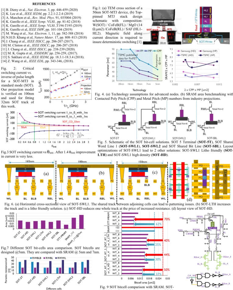
Due to its superior scaling properties and non-volatility, STT-MRAM is presently being commercialized as a replacement for slow SRAMs and eFlash in embedded cache memories, with potential applications also as persistent DRAM [1,2]. However, it will be ultimately limited to last level caches (LLCs) due to the read disturb and endurance issues when operating <10ns. Alternatively, SOT-MRAM [3] offers unmatched switching speed and endurance compared to STT-MRAM. In such devices (Fig.1), write (SOT) and read (TMR) path are separated, and the 3-terminal cell structure minimizes risk of voltage break down leading to reliable ns and sub-volt operations [4]. With these benefits, SOT-MRAM can potentially replace HP and HD SRAM at register, L1 and L2 level in CPUs, GPUs and NPUs in the embedded domain.
However, there are certain challenges facing SOT technology with regards to density (3T cell) and write current (material efficiency), as presently, the required SOT critical
switching current (ISOT) is around one order larger than
STT-MRAM. In this work, we tackle such important challenges limiting the adoption of SOT as the embedded memory of choice (compared to SRAM and STT-MRAM), based on SOT and silicon measurement data. To this end, we perform extensive DTCO on different SOT-MRAM bit-cells to arrive at optimized solutions for the Performance, Power and Area (PPA). This is followed by macro designs at 5nm node with associated design-level PPA analysis, demonstrating two important factors limiting the SOT macro level performance to max ~1GHz at advanced nodes – i) a saturation of SOT write
current with increasing SOT efficiency θSHE, and ii) Bit-line
(BL) parasitics specifically resistance.
II. SOTMRAM TECHNOLOGY
A typical SOT-MTJ device structure is shown Fig. 1. It consists of top-pinned perpendicularly magnetized MTJ
patterned on a thin SOT metal channel (here 3.5nm of Wβ). To
operate such device, SOT current needs to be assisted by a static in-plane magnetic field in the same direction to ensure efficient deterministic switching [4, 5]. Nowadays, various solutions have been proposed to operate the device in the absence of external field [5,6], and major challenges are relegated to MTJ performance (retention, stop etch) [7] and writing efficiency. In
fact, in Fig.2, we present SOT critical switching current (ISOT)
as a function of inverse of pulse length (τp) in sub-ns regime.
One can see that it requires ~500uA to switch at 1ns, which scales to 200uA at 32nm according to our models. As shown by
ISOT equation (Fig. 3), a direct path for reducing write operation
of SOT-MRAMs such as minimizing transistor wear on bit cell is to improve the conversion ratio between charge and spin
currents θSHE. Typical SOT metals allow θSHE =0.1-0.5 [3,5],
while θSHE>1 would be required to achieve sub-100 µA currents
(Fig. 3), which requires new materials such as topological insulators [8], which unfortunately are currently immature for technology and challenging to be integrated in fab environment.
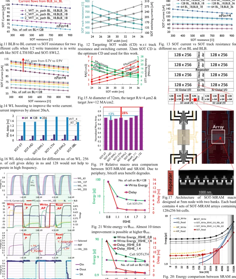
III. DESIGN TECHNOLOGY CO-OPTIMIZATION For an efficient embedded memory design, accurate technology assumptions extensive DTCO is important. Hence, we combine the device sizing constraints of different foundries and IMEC Silicon data to estimate the SRAM area [9-12] at 5nm CMOS node (Fig. 4). The Contact Poly Pitch (CPP) and Metal Pitch (MP) numbers are estimated accordingly with CPP=45nm based on our technology and models [13].
A. SOT bitcell optimisation
High ISOT requirements and separate RD/WR selectors
places limitations on the bit-cell from the FEOL point of view. In addition to this, the SOT bit-cell (SOT-5T) [14] utilizes 2 selectors with RD/WR word-lines (WLs), BLs and WR bit-line bar (BLB). Routing these 5 signals restricts cell scaling from BEOL point of view. SOT cell height is mostly determined by BEOL patterning, while FEOL dominates in SRAM. Keeping in mind these limitations, we propose three bit-cell solutions (Fig. 5): SOT Shared WL1 (SOT-SWL1), SOT-SWL2 and SOT Shared BL (SOT-SBL). Moreover, layout optimizations of SOT-SWL1 lead to two additional solutions: SOT-SWL1 Litho friendly (SOT-LTH) and SOT-SWL1 HD (SOT-HD).
In the SOT-SWL1 [5.5 tracks] layout (Fig. 6 (a)), cell height is defined by the space between the WL MINT (MT) track and RBL MT track. Here, while the WL is shareable, RBL is not,
leading unequal spacing between SOT tracks in a row and thus, patterning issues. As a solution, we increase the tracks in SOT-LTH to 6 for equal spacing between SOT tracks in a row (lithography friendly solution; Fig. 6(b)) which affect bit-cell size. The SOT-HD solution reduces the whole track at the cost of increased resistance (Fig. 6c). Fig. 7 shows he area comparison between proposed SOT bitcell solutions, HD SRAM and STT. We see that SOT-SWL1 variants (SWL1, LTH and HD) and SOT-SWL2 are the most favorable and since SWL1 causes patterning issues, it is not an optimal solution.
In addition, Fig.8 depicts the BL/BLB Resistance per cell for the different SOT bit-cells. HD, 5T and SOT-SBL have 36Ω/cell BLB res (single MT track for BLB), while all bit-cells have BL res of 18Ω/cell since 2 tracks are connected to the BL (M2 and MT track). Thus, we have 2 cases of BL/BLB res: 18/18 and 18/36. WL res is proportional to cell height. SOT-SBL has a high WL and BL/BLB res (42 and 18/36 Ω/cell respectively), which is not suitable for our target. Consequently, SOT-LTH, SOT-HD and SOT-SWL2 remain the best solutions for HD and HP targets at advanced nodes.
Cell-size variation with FEOL-size required for ISOT (Fig. 9)
shows that SOT-HD has an area gain of 37% w.r.t 111 SRAM, and SOT-LTH has a 40% area benefit w.r.t 122 SRAM. This is retained when going from 2 to 4 fins for the Read Transistor (RT) and 2 to 6 fins for the Write Transistor (WT) showing that SOT bit-cell area is more limited by BEOL rather than FEOL.
B. Read-Write optimisation
A typical SOT cell has two NFETs independently selecting RD and WR paths (Fig. 10). One can set the magnetic field such
that ISOT from BL to BLB leads to a Parallel to Antiparallel
(P/AP) transition, such that the WT is in conduction mode and offers the lowest resistance. When current flows from BLB to BL, the WT degenerates due to source resistance (and SOT track resistance). In case of SOT-SWL2 (Fig. 11), both WTs deal with source degeneration limitation (one in P/AP and other in AP/P). This is not realistic for efficient WR and limit bit-cell solutions to SOT-LTH and SOT-HD for HP and HD target.
As mentioned above, ISOT is limited by the track resistance
(related to SOT resistivity and dimensioning). The SOT track width/Critical Dimension (CD) is in turn governed by MINT track pitch (where maximum available space = 2 x MINT pitch: Fig. 6) and MTJ CD (SOT CDminimum = MTJ CD). Thus, the available range for SOT CD is from 24nm to 36nm. Fig. 12 shows that with increasing SOT CD, track resistance reduces
(at the cost of ISOT). At the optimum SOT CD of 32nm, track
resistance and ISOT are 500Ω and 210uA (0.225 θSHE)
respectively. ISOT also depends upon BL/BLB resistance. Fig.
13 shows the relationship between BL/BLB resistance and its loading with SOT track resistance. Less loading along with low BL/BLB res (18/18Ω/cell) deliver highest possible current and lowest switching time but increases area overhead at array level (due to increased periphery). 128 is the optimum BL loading and can deliver 92µA at 32nm CD (for low BL/BLB res). To speed-up SOT switching further, the current passing through SOT can be increased in 2 ways: 1) Increasing the fins of the WT (increase in bit-cell area) and 2) boosting the VG of the WT (favorable). Fig. 14 shows that WL boosting from 0.7 to 0.9 can increase WT current from 92uA to 112uA. However, it requires
at-least 210µA to switch the SOT cell for θSHE of 0.225 and SOT
CD of 32nm. From Fig. 3, we require a θSHE of 0.8 (100uA ISOT
for 1ns switching) for SOT-LTH and a 1.4 θSHE (65uA ISOT for
1ns switching) for SOT-HD.
IMTJ is the RD current used for sensing the MTJ state (at
VREAD). Fig. 15, gives the RA and (STT switching current
density) JSW for our range of SOT CD values, assuming MTJ
CD = SOT CD. A JSW(STT) greater than 10MA/cm2 for the
target RA of 4Ω.um2 is required, which is almost 2x the STT
target at 5nm node [13].
IV. MACRO DESIGN
The WL delay vs loading is shown in Fig. 16 for different SOT cells. We require a loading of 64 on WL with repeaters (256 total) to operate at GHz frequencies. Fig. 17 shows our Macro architecture. The 32 KB SOT macro is divided into 2 banks with a simple butterfly architecture for each 16KB bank that is divided into 4 sub banks. The sub bank has a maximum size of 32Kb (128 rows x 256 columns) with shared local IOs for top and bottom arrays. The 16KB bank is repeated using repeater logic between 2 banks. For the TT corner of the device (and MTJ pillar), switching events are captured in Fig. 18. 75uA current flows during AP/P and 92uA during P/AP transitions. The reduction in WT current is due to the drop across WR
driver. θSHE for this simulation is 1.4. BL res is crucial here,
since at SOT track res of 500Ω (for 32nm SOT CD), most of the voltage drops across BL, limiting WR current and speed. A single-ended sensing scheme (Fig.9) for sensing the MTJ state at 25uA RD current leads to a RD delay of 0.9ns.
V. PPA ANALYSIS AND CONCLUSION
Fig. 19 and 20 highlight the comparison between SRAM and SOT Macros for the embedded domain at 5nm node for area and energy consumption, respectively. Adding repeaters between sub banks to operate at high frequency comes at the cost of leakage as well as area. Fig. 19 shows that the SOT-HD Macro has an area benefit of ~13% and ~30% w.r.t HD and HP SRAM, whereas the SOT-LTH Macro has an area benefit of 6% and 25% w.r.t HD and HP SRAM. The SOT-LTH design manages to achieve a nominal RD/WR access latency ~0.9/1.4ns. A closer look at the energy profile (Fig. 20) reveals 3 major crossover zones that can impact energy consumption. SOT-MRAM RD becomes more energy efficient as compared to HP-SRAM @0.4MB (max L1 capacity) and crosses HD-SRAM @2MB/8MB for RD/WR, due to the exponential increase of SRAM standby power with increasing capacity.
In conclusion, at LLC capacities in present embedded HPC and some Mobile systems (<8MB), SOT-MRAM is clearly
more beneficial regardless of its present high write current. θSHE
and BL Resistance are knobs affecting ISOT, and thus energy and
delay. By exploring the variation of these parameters with respect to energy and delay (Fig. 21 and Fig. 22), we clearly show that SOT-MRAM is penalized due to higher BL resistance that leads to higher drop across BL. Our work shows
that achieving lower BL resistance at lower nodes with θSHE ~
0.8 would improve considerably energy and delay, by more than 10X, making SOT-MRAM a credible solution for future LLC applications.
Acknowledgement: This work was supported by IMEC’s Industrial Affiliation Program on Memory Design.
REFERENCES
[1] B. Dieny et al., Nat. Electron. 3, pp. 446-459 (2020) [2] K. Lee et al., IEEE IEDM, pp. 2.2.1-2.2.4 (2019) [3] A. Manchon et al., Rev. Mod. Phys. 91, 035004 (2019) [4] K. Garello et al., IEEE Symp. VLSI , pp. 81-82 (2018) [5] K. Garello et al., IEEE Symp. VLSI ,T194-T195 (2019) [6] K. Garello et al, IEEE IMW, pp. 101-104 (2019)
[7] M. Wang et al., Nat. Electron. 1, 11, pp. 582-588 (2018) [8] N.H.D. Khang et al, Nature Mater. 17, pp. 808–813 (2018) [9] J. Chang et al., IEEE ISSCC, pp. 206-207 (2017). [10] M. Clinton et al., IEEE ISSCC, pp. 206-207 (2018) [11] J. Chang et al., IEEE ISSCC, pp. 238-239 (2020). [12] M. K. Gupta et al., ESSDERC pp. 256-259, (2017). [13] S. Sakhare et al., IEEE IEDM, pp. 18.3.1-18.3.4 (2018). [14] Z. Wang et al., IEEE EDL, pp. 343-346, (2018).
Fig.1: (a) TEM cross section of a 50nm SOT-MTJ device, (b) Top-pinned MTJ stack design schematic with composition: W(SOT) / CoFeB(FL) / MgO (14 Ω.μm2) /CoFeB(RL) / SAF (HL1-HL2). Magnetic field along current direction is required to insure deterministic switching [1].
Fig. 2: Critical switching current vs. inverse of pulse length for a SOT-MTJ in standard mode (SOT). Our projection model is verified on 100nm and used for fitting 32nm SOT track of this work.
Fig. 4. (a) Technology assumptions for advanced nodes. (b) SRAM area benchmarking with Contacted Poly Pitch (CPP) and Metal Pitch (MP) numbers from industry projections.
20 30 40 50 60 70 80 90 20nm 16nm 10nm 7nm 5nm Pa ra me te r [ nm] Technology FP MP CPP As su m pt io ns @ 5nm TSMC published data for FinFET
5.5 6 6.5 7 7.5 8 8.5 9 9.5 0.002 0.007 0.012 SR AM/2 x CP P x MP 2 x CPP x MP [um2] Samsung (HD) Samsung (HP) TSMC (HD) TSMC (HP)
Fig.3 SOT switching current vs θSHE. After 1.4 θSHE improvement
in current is very less.
Fig. 5. Schematic of the SOT bit-cell solutions. SOT 5 Terminal (SOT-5T), SOT Shared Word Line 1 (SOT-SWL1), SOT-SWL2 and SOT Shared Bit Line (SOT-SBL). Layout optimizations of SOT-SWL1 lead to 2 other solutions: SOT-SWL1 Litho friendly
(SOT-LTH) and SOT-SWL1 high density (SOT-HD). BL WL RWL RBL BLB Total Fin=4 Total Fin=2
SOT-5T SOT-SWL1 SOT-SWL2 SOT-SBL
BL WL RBL BLB Total Fin=4 Total Fin=2 BL WL RWL BL BLB Total Fin=4 Total Fin=2 BL WL RBL BLB WL Total Fin=4
Fig. 6. (a) Horizontal cross-sectional view of SOT-SWL1. The shared track between adjoining cells can lead to patterning issues. (b) SOT-LTH increases the track and is a litho friendly solution. (c) SOT-HD reduces one whole track at the price of increased resistance. (d) layout view of SOT-HD.
BE BE ME HM M3 (WL) SOT MT MT M1 MT M1 MT MT MT M1 M2 M2 M2 TE WL BL BLB RBL 165nm M2 M2 M2 18 BE BE ME HM M3 (WL) SOT MT MT M1 MT M1 MT MT MT M1 M2 M2 M2 TE WL BL BLB RBL MT WL M2 M2 M2 M2 180nm BE BE ME HM M3 (WL) SOT MT MT M1 MT MT MT MT M1 M2 M2 M2 TE WL BL WL BLB RBL M2 M2 M2 150nm M1 M1 M1 M1 M1 M1 M2 M2 M2 M2 M2 M2 SO T M1 M2 M2 M2 M2 M2 M2 SO T M3 M3 WL MTJ
Fig.7 Different SOT bit-cells area comparison. SOT bitcells are designed @5nm. They are compared with SRAM @ 5nm and 7nm.
0 0.0050.01 0.0150.02 0.0250.03 Ar ea [um 2]
Fig.8 BL/BLB resistance comparison among different SOT bit-cells. WL resistance is proportional to cell height. Bit-line resistance can split in two cases. BL/BLB=18/18Ω/cell and BL/BLB=18/36Ω/cell. 0 10 20 30 40 50 Par asit ic r esist an ce /c el l [Ω ] Different cells RWBLB RWBL RWWL (a) (b) (c) (d)
Fig. 10. Schematic of RD and WR path for SOT-MRAM.
Far cell BL_A BL_B BLbar_A BLbar_B CLK_WE Din SEL SEL SOT cellMT J BL_A BL_B BLbar_A BLbar_B RRWL CRWL RB L CB L RB LB CB LB RWWL CWWL RR BL CR B L BLB RBL BL BL WWL RWL
Fig. 9 SOT bitcell comparison with SRAM. SOT-MRAM cell height is governed by BEOL patterning on contrary to SRAM cell that is why even more no. of fin for Write Transistor (WT) will not increase area in some cases.
0 0.006 0.012 0.018 0.024 0.03 WT_2 WT_4 WT_6 WT_8 WT_2 WT_4 WT_6 WT_8 WT_2 WT_4 WT_6 WT_8 111 122 WT_2 WT_4 WT_6 WT_8 SO T_ R T _2 _ or _4 _H D SO T_ RT_ 2_ or _4 SO T _RT_ 2_ or _4 _LT H SR A M ST T -MR A M
Bitcell area [um2] 37% 30% 25% 62% 70% 40% 44% 50%
↑
Fig. 12 Targeting SOT width (CD) w.r.t track resistance and switching current. 32nm SOT CD is the optimum CD and used for this work.
100 135 170 205 240 275 310 300 400 500 600 700 800 900 24 26 28 30 32 34 36 SO T s w itc hin g cu rr en t [u A] SO T tr ac k r es is tanc e [Ω ] SOT width [nm]
Fig. 13 SOT current vs SOT track resistance for different no. of on BL and BLB.
20 40 60 80 100 120 140 160 180 300 400 500 600 700 800 900 SO T Cur re nt [uA] SOT resistance [Ω] 256 BL_18,BLB_18 256 BL_18,BLB_36 128 BL_18,BLB_18 128 BL_18,BLB_36 64 BL_18,BLB_18 64 BL_18,BLB_36 nFin=4
Fig.14 WL boosting to improve the write current. Current improves by almost 20uA.
55 65 75 85 95 105 115 300 400 500 600 700 800 900 SO T C urr en t [u A ] SOT resistance [Ω] nFin=4 No. of cell on BL=128 WL goes from 0.7V to 0.9V
Fig.15 At diameter of 32nm, the target RA≈4.μm2 & target Jsw=12 MA/cm2. 0 4 8 12 16 20 24 28 2 3 4 5 6 7 8 24 26 28 30 32 34 36 ST T s w itc hing de nsit y [M A /c m 2] RA [Ω -c m 2] SOT width [nm]
Fig.11 BLB to BL current vs SOT resistance for two different cells when 1/2 write transistor is in write path like SOT-LTH/HD and SOT-SWL2.
65 70 75 80 85 90 95 100 105 300 400 500 600 700 800 900 SO T C urre nt [ uA ] SOT resistance [Ω] 1_WT_in_path BL_18,BLB_36 1_WT_in_path BL_18,BLB_18 2_WT_in_path BL_18,BLB_18 No. of cell on BL=128
Current flows from BLB_to_BL
nFin=4
Fig.16 WL delay calculation for different no. of on WL. 256 no. of cell gives delay in ns and 128 would not help to operate in high frequency.
0 0.4 0.8 1.2 1.6 2 WL d el ay [ ns ] 64 128 256 WT_4 _RT_2
Fig. 19 Relative macro area comparison between SOT-MRAM and SRAM. Due to periphery, bitcell area benefit degrades.
0 0.1 0.2 0.3 0.4 0.5 0.6 0.7 0.8 0.9 1 No rm al is ed Ma cr o A rea 13% 25%
Fig.17 Architecture of SOT-MRAM macro designed at 5nm node with two banks. Each bank contains 4 sets of SOT-MRAM arrays containing 128x256 bit-cells.
Fig.18 Simulated write operation where AP2P and P2AP happens at 1.4 ns time-period (Ist and IIIrd cycle). 100mV
differential is generated to sense the state of the cell. 1.4ns pulse is used for simulation (both write and read). However, read can be possible at 0.9ns.
0 0.2 0.4 0.6 0.8 1
0 1.4E-09 2.8E-09 4.2E-09 5.6E-09
Volt ag e [ V ] WL_63 WL_127 WL_191 WL_255 0 0.1 0.2 0.3 0.4 0.5 0.6 0.7 0.8 0.9
0 1.4E-09 2.8E-09 4.2E-09 5.6E-09
Volt ag e [ V ] Selected REF WL_255 0 0.125 0.25 0.375 0.5 0.625 0.75 0.875 1 -100 -75 -50 -25 0 25 50 75 100
0 1.4E-09 2.8E-09 4.2E-09 5.6E-09
Vo lta ge Cur ren t
SL Current (uA) MTJ state WL_255 BL BLB
0 0.1 0.2 0.3 0.4 0.5 0.6 0.7
0 1.4E-09 2.8E-09 4.2E-09 5.6E-09
V ol tage [ V ] Time [s] Din Dout SA V_Antiparallel V_Parallel WL delay Write
_P Read_P Write_AP Read_AP
Read
_P Read_AP
Fig. 21 Write energy vs θSHE. Almost 10 times
improvement is possible at higher θSHE. 0 2 4 6 8 10 12 14 16 1 10 100 0.8 1.1 1.4 1.7 2 De la y [ ns ] Ene rg y [ pJ ] θSHE Write Energy Delay No. of cell on BL=128 Cell: SOT-LTH
Fig. 20: Energy comparison between SRAM and SOT-MRAM for varying sizes. SOT-MRAM read becomes more energy efficient compared to HP SRAM @0.4MB and crosses HD-SRAM around 2MB. SOT-MRAM write crosses HD-SRAM in the range of 8MB to 16MB depending on θSHE (θSHE ↑ crossingpoint ↓ and vice versa).
Fig. 22 Write energy vs RBL. Even at higher
θSHEit could be possible to achieve higher
frequency for the same memory size by reducing BL resistance. 0 2 4 6 8 10 12 14 16 0.9 9 90 18 15 12 9 6 De la y [ ns ] En er gy [p J] BL Resistance/cell [Ω] Write Energy_θSHE_0.8 Write Energy_θSHE_1.4 Delay_θSHE_0.8 Delay_θSHE_1.4 No. of cell on BL=128 Cell: SOT-LTH