Publisher’s version / Version de l'éditeur:
Applied Physics Letters, 96, 24, pp. 243104-1-243104-3, 2010-01-01
READ THESE TERMS AND CONDITIONS CAREFULLY BEFORE USING THIS WEBSITE. https://nrc-publications.canada.ca/eng/copyright
Vous avez des questions? Nous pouvons vous aider. Pour communiquer directement avec un auteur, consultez la première page de la revue dans laquelle son article a été publié afin de trouver ses coordonnées. Si vous n’arrivez pas à les repérer, communiquez avec nous à PublicationsArchive-ArchivesPublications@nrc-cnrc.gc.ca.
Questions? Contact the NRC Publications Archive team at
PublicationsArchive-ArchivesPublications@nrc-cnrc.gc.ca. If you wish to email the authors directly, please see the first page of the publication for their contact information.
NRC Publications Archive
Archives des publications du CNRC
This publication could be one of several versions: author’s original, accepted manuscript or the publisher’s version. / La version de cette publication peut être l’une des suivantes : la version prépublication de l’auteur, la version acceptée du manuscrit ou la version de l’éditeur.
For the publisher’s version, please access the DOI link below./ Pour consulter la version de l’éditeur, utilisez le lien DOI ci-dessous.
https://doi.org/10.1063/1.3454923
Access and use of this website and the material on it are subject to the Terms and Conditions set forth at
Self-organized phase segregation between inorganic nanocrystals and
PC61BM for hybrid high-efficiency bulk heterojunction photovoltaic
cells
Tsang, Sai-Wing; Fu, Huiying; Ouyang, Jianying; Zhang, Yanguang; Yu, Kui;
Lu, Jianping
https://publications-cnrc.canada.ca/fra/droits
L’accès à ce site Web et l’utilisation de son contenu sont assujettis aux conditions présentées dans le site LISEZ CES CONDITIONS ATTENTIVEMENT AVANT D’UTILISER CE SITE WEB.
NRC Publications Record / Notice d'Archives des publications de CNRC:
https://nrc-publications.canada.ca/eng/view/object/?id=6997dd76-c589-466c-83b1-288ea309d5a8 https://publications-cnrc.canada.ca/fra/voir/objet/?id=6997dd76-c589-466c-83b1-288ea309d5a8Self-organized phase segregation between inorganic nanocrystals and
PC
61BM for hybrid high-efficiency bulk heterojunction photovoltaic cells
Sai-Wing Tsang,1Huiying Fu,1Jianying Ouyang,2Yanguang Zhang,1Kui Yu,2 Jianping Lu,1,a兲 and Ye Tao1,a兲
1
Institute for Microstructural Sciences (IMS), National Research Council of Canada, Ottawa, Ontario K1A 0R6, Canada
2
Steacie Institute for Molecular Sciences (SIMS), National Research Council of Canada, Ottawa, Ontario K1A 0R6, Canada
共Received 18 March 2010; accepted 24 May 2010; published online 16 June 2010兲
We demonstrate a simple approach to generate phase segregation between colloidal PbS nanocrystals 共NCs兲 and organic 关6,6兴-phenyl C61 butyric acid methyl ester 共PC61BM兲. Continuous
vertical phase segregation is observed in cross-linked composite films of NCs and PC61BM. Hybrid
bulk heterojunction photovoltaic cells fabricated with the phase segreated composite layer have achieved the state-of-art power conversion efficiency of 3.7% under one sun of simulated Air Mass 1.5 Global solar irradiation. The presented method can be generally applied in other NC/organic systems for the development of hybrid heterojunction photovoltaic cells. 关doi:10.1063/1.3454923兴
Photovoltaic 共PV兲 cells based on solution processable colloidal nanocrystals 共NCs兲 and organic semiconductors have drawn a lot of attention recently, owing to their low fabrication cost, large area capability, high optical absor-bance, and the potential for high power conversion efficiency 共PCE兲.1,2In addition, due to the quantum confinement effect, the optoelectronic properties of the NCs can be tuned by varying the size and shape of the NCs during the synthesis. Therefore, the optical absorption of NCs can cover a broader spectral range, from the visible to the infrared, offering op-timal light absorption for PV applications. Due to the complementary optical absorption properties and the solution processability, NC/organic hybrid PV cells have attracted in-creasing research interests. However, most of such hybrid PV cells have PCEs of only around 2% or lower.3In most of those hybrid systems, the NCs are homogeneously dispersed in a polymer matrix. Due to the energy difference between the two materials and the absence of continuous phases of the NCs, at least one type of the charge carriers 共electron or hole兲 is trapped inside the NCs with a long hopping distance to the adjacent NCs, which significantly reduces the photo-current in the device. An efficient hybrid PV cell was dem-onstrated with an impressive PCE of 2.6% by using a blend of CdSe nanorods and poly共3-hexylthiophene兲 and a solvent with slow evaporation rate to enhance the self-organization of the polymer.4The approach is similar to the bulk hetero-junction concept used in the polymer PV cells,5,6where the organic electron donor and acceptor materials form nano-scale interpenetrating networks which facilitate exciton dis-sociation and charge transport across the whole active layer. However, the lack of a continuous vertical distribution of the CdSe nanorods in the vertical direction makes it inefficient to extract the dissociated electrons from the system. It is well known that initiating and controlling the nanoscale phase segregation in a blend of electron donor and acceptor mate-rials is a key to optimizing the device performance with so-lution processable PV materials.
In this work, a fast and simple method is demonstrated to develop hybrid bulk heterojunction PV cell with colloidal PbS NCs and organic 关6,6兴-phenyl C61 butyric acid methyl
ester 共PC61BM兲. Phase segregation and continuous vertical
phases of the PbS NCs and PC61BM are obtained by simply
cross-linking the composite film at room temperature for a few minutes. The size of the segregated domains can be con-trolled with different weight 共wt.兲 ratios between the PbS NCs and PC61BM. As compared to the bilayer device
fabri-cated from the same two materials, the bulk heterojunction approach has improved the PCE from 3.1% to 3.7%, which is attributed to the significant increase in the device’s short circuit current 共JSC兲 from 7.61 to 10.01 mA/ cm2. Improved
exciton dissociation in the bulk heterojunction device is evi-dent from the internal quantum efficiency 共IQE兲. We believe that this method can be generally applied to different colloi-dal NCs/organic systems and will facilitate the development of hybrid bulk heterojunction PV cells.
For the PV cell fabrication, indium tin oxide 共ITO兲 coated glass was used as the anode. Immediately prior to device fabrication, the ITO glass was cleaned by ultrasonic baths of organic solvents 共acetone and isopropanol兲 and then UV-ozone treated for 15 min. Oleic acid capped PbS NC 共PbS-OA兲 solution in chloroform 共5 mg/mL兲 was used to prepare the active layer. 1,3-benezendithiol 共BDT兲 was used as the cross-linker to replace the OA surface ligand and bridge the NCs. Details about the NC synthesis, preparation of cross-linked PbS NC only films and device characteriza-tion are discussed in the supplementary materials.7 For the bulk heterojunction devices, a solution of a mixture of PbS-OA NC and PC61BM in chloroform was spun 共2500 rpm
for 1 min兲 on top of a NC only layer to form a composite layer. The sample was then soaked in the cross-linker solu-tion for 10 min to facilitate the phase segregasolu-tion between the PbS NCs and the PC61BM molecules. It was followed by
a spin-coating 共2500 rpm, 1 min兲 the solution of PC61BM in
chloroform 共10 mg/mL兲 on top of the composite layer. Af-terwards, the sample was transferred to an evaporation cham-ber without exposure to the air. Finally, 1 nm of LiF and 120 nm of Al were thermally evaporated on top of the a兲
Authors to whom correspondence should be addressed. Electronic ad-dresses: ye.tao@nrc-cnrc.gc.ca and jainping.lu@nrc-cnrc.gc.ca.
APPLIED PHYSICS LETTERS 96, 243104 共2010兲
0003-6951/2010/96共24兲/243104/3/$30.00 96, 243104-1
PC61BM to form the cathode. The PV cells had a general
structure of ITO/active layer/LiF 共1 nm兲/Al 共120 nm兲 with an active area of 9 mm2. The device structures used in this study are summarized in Table I.
Figure1shows the atomic force microscopy 共AFM兲 im-ages of the cross-linked PbS NC only and composite films with different wt. ratios of PbS NCs and PC61BM. Phase
segregation of BDT linked PbS 共PbS-BDT兲 NCs and PC61BM molecules in the cross-linked composite films have
been observed. Figure1 shows the surface morphologies of the cross-linked PbS-BDT only 关Fig. 1共a兲兴 and cross-linked PbS-BDT: PC61BM composite films prepared from solutions
with PbS-OA: PC61BM wt. ratios of 50:1, 30:1, and 10:1
关Figs.1共b兲–1共d兲兴, respectively. The films have similar surface roughness less than 3 nm. Szendrei et al. demonstrated that a mixture of PbS NCs capped with OA 共PbS-OA兲 and PC61BM
forms a homogeneous film without phase segregation.8 Inter-estingly, as shown in the corresponding phase images 关Figs.
1共e兲 and 1共h兲兴 acquired in situ with the surface morpholo-gies, segregated PbS-BDT 共bright region兲 and PC61BM 共dark
region兲 domains are clearly present in our cross-linked com-posite films. During the cross-linking process, the OA sur-face ligands are replaced by the more reactive BDT cross-linker molecules. The two sulfur atoms in a BDT molecule can each form a strong bond with the surface Pb atoms of neighboring NCs and, therefore, bridge the NCs together. Since the size of BDT molecule is much smaller than that of OA, the cross-linking reaction can bring the NCs much closer and in the meanwhile expel PC61BM out of the NC
domains. In addition, the sizes of PbS-BDT and PC61BM
domain can also be controlled by using different wt. ratios of PbS-OA: PC61BM. With increasing PC61BM content in the
composite film, the PC61BM domains gradually emerge from
the large PbS-BDT domains and eventually clusters of NCs
and PC61BM are formed. Such a phase segregated structure
substantially increases the interfacial area between the two materials. In is worth noting that the small domains of PC61BM trapped in the NCs matrix, especially with wt.
ra-tios 50:1 and 30:1, make the PC61BM difficult to be
redis-solved by the upper spin-coated layer, which is advantageous for preparing multilayer structures.
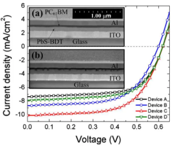
We fabricated hybrid bulk heterojunction PV cells with the cross-linked composite layer approach. With the same materials a bilayer device was also fabricated for compari-son. The inset of Fig. 2 shows the cross-section scanning electron microscopy 共SEM兲 images of bilayer device A 关Fig.
2共a兲兴 and bulk heterojunction device C 关Fig. 2共b兲兴. For the bilayer heterojunction device, layers of PbS-BDT and PC61BM with an abrupt interface are clearly resolved
be-tween the ITO and Al electrodes. For the bulk heterojunction device, between the pure PbS-BDT and PC61BM layers, a
cross-linked composite layer is observed, which contains in-terpenetrating networks of PbS-BDT and PC61BM. Such
bulk heterojunction device benefits from a few structural ad-vantages as follows: larger contact area between the PbS-BDT and PC61BM domains increases the probability of
ex-citon dissociation in both NCs and organics; the formation of interpenetrating donor and acceptor networks reduces the distance for the photogenerated excitons to diffuse to the heterojunction for dissociation; the composite film is sand-wiched between two buffer layers of pristine PbS-BDT and PC61BM, which suppresses the resistivity current under
for-ward voltage bias; and more importantly, the continuous ver-tical phases of PbS-BDT and PC61BM in the composite film
can facilitate the transport of the dissociated holes and elec-trons, respectively.
The PbS NCs used to fabricate the hybrid heterojunction devices are optimized with size and quality as discussed in the supplementary materials.7A NC only Schottky-type PV cell was fabricated with the same batch of NCs to evaluate the quality of the NCs. The device demonstrated a PCE of 3.2% under one sun of simulated Air Mass 1.5 Global 共AM 1.5 G兲 solar irradiation. Figure2 shows the current density– voltage 共J − V兲 characteristics of the PbS-BDT/ PC61BM
bi-TABLE I. Summary of device structures used in this study. The devices have a general structure of ITO/PbS-BDT共40 nm兲/composite layer 共40 nm兲/PC61BM 共40 nm兲/LiF 共1 nm兲/Al.
Device Composite layer
A PbS-BDT共40 nm兲
B PbS-BDT: PC61BM共wt. ratio 50: 1兲
C PbS-BDT: PC61BM共wt. ratio 30: 1兲
D PbS-BDT: PC61BM共wt. ratio 10: 1兲
FIG. 1. 共Color online兲 AFM images of the cross-linked PbS NC only and cross-linked composite films casted from solutions with different wt. ratios of PbS NCs and PC61BM molecules. The upper images 共a兲, 共b兲, 共c兲, and 共d兲
indicate the morphology of the cross-linked films prepared with PbS NC only and different wt. ratios of PbS-OA: PC61BM 50:1, 30:1, and 10:1
re-spectively. The lower images 共e兲, 共f兲, 共g兲, and 共h兲 which, respectively, cor-responding to the morphology images 共a兲, 共b兲, 共c兲, and 共d兲, represent the in situphase images. All images have the scan range of 1 ⫻ 1 m2.
FIG. 2. 共Color online兲 Measured current J − V characteristics under one sun of simulated AM 1.5 G solar irradiation of the bilayer device A 共black; square兲 and the bulk heterojunction devices B 共blue; circle兲, C 共red; up-triangle兲, and D 共green; down-triangle兲 with different wt. ratios between PbS NCs and PC61BM. Inset shows the cross-section SEM images of 共a兲 the
bilayer ITO/ PbS-BDT/ PC61BM/ LiF/ Al device A and 共b兲 the bulk
hetero-junction ITO/ PbS-BDT/ PbS-BDT: PC61BM共wt. ratio 30: 1兲 / PC61BM/
LiF/ Al device C.
243104-2 Tsang et al. Appl. Phys. Lett. 96, 243104 共2010兲
layer and the bulk heterojunction PV cells under one sun of simulated AM 1.5 G solar irradiation. Details of the PV cell structure and performances are summarized in Table I and Table II, respectively. Generally, the heterojunction devices have larger open circuit voltage 共VOC兲, 0.58–0.60 V, and
fill-factor 共FF兲, 63%–67%, than the NC only Schottky-type de-vice 共VOC= 0.56 V and FF= 53%兲. It is attributed to the fact
that the VOCof a Schottky solar cell is limited to one half of
its energy gap while the VOC of a heterojunction device is
not, and that the additional PC61BM layer that efficiently
prevents excitons from quenching at the NC/metal interface, as reported in a similar system of PbS NC/ C60 bilayer
device.9As compared to the bilayer device A, the bulk het-erojunction devices B–D have larger short circuit current 共JSC兲. The JSCis increased from 7.34 mA/ cm2 in device A
to 10.10 mA/ cm2in device C. As a result, a maximum PCE
of 3.7% has been achieved in the bulk heterojunction device with the optimal wt. ratio of 30:1 between PbS NCs and PC61BM. Using the measured external quantum efficiency
共EQE兲 data, we calculated the JSC under 100 mW/ cm2 of
AM 1.5 G solar irradiation as listed in Table II. The calcu-lated values are consistent with the JSC measured from the
J− V results, demonstrating negligible spectral mismatch in the PCE measurement. The increase in JSCin the bulk
het-erojunction devices is attributed to the improved exciton dis-sociation with the interpenetrating networks of PbS NCs and PC61BM as discussed above. Moreover, the dependence of
JSC on the wt. ratios between the NCs and PC61BM also
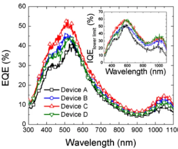
indicates that the exciton dissociation efficiency in the com-posite film is controlled by the domain size of the individual material. Such phenomenon is widely observed in polymer bulk heterojunction PV devices.10,11 It is also worth noting that the series resistance RS of the bulk heterojunction
de-vices are similar to that of the bilayer device, neither the electron nor holes are trapped in the composite layer. It sup-ports the argument of continuous vertical phase segregation as observed in the SEM measurement. The improved exciton dissociation efficiency in the bulk heterojunction devices is supported by the device quantum efficiency. As shown in Fig. 3, the measured EQE with a maximum of 40% in the bilayer device is increased to over 50% in the bulk hetero-junction device. The IQEs 关IQE= EQE/ 共1 – R兲兴 calculated using the EQE and device reflectance data are shown in the inset in Fig.3. The IQEs of the bulk heterojunction devices have been increased in the whole spectral range. It further supports that the observed improvements in EQE and JSCare
not due to the optical difference in the devices but because of the more efficient exciton dissociation in the bulk hetero-junction structure.
In conclusion, cross-linking induced phase segregation in the composite thin film of PbS NCs and PC61BM has been
demonstrated. The presented approach facilitates the fabrica-tion of hybrid NC/organic bulk heterojuncfabrica-tion PV cell with continuous phase segregation of individual material. The re-sulting solution-processed hybrid bulk heterojunction device has achieved a very promising PCE of 3.7% under one sun of simulated AM 1.5 G solar irradiation and improved EQE in a wide spectral range. The presented technique is expected to have wide applications in different NC/organic systems for the development of hybrid bulk heterojunction PV cells. The authors would like to thank Hsien-Tse Tung, Dr. Xiaohua Wu, and Jeffrey W. Fraser for their experimental support. Valuable discussion on NC synthesis with Dr. Ruib-ing Wang is highly appreciated. The authors would also like to acknowledge the financial support from the National Re-search Council of Canada’s NRC-Nano Initiative. H. Fu thanks the Chinese Scholarship Council for providing her PDF scholarship.
1
G. Dennler, M. C. Scharber, T. Ameri, P. Denk, K. Forberich, C. Waldauf, and C. J. Brabec,Adv. Mater. 共Weinheim, Ger.兲 20, 579 共2008兲. 2
M. C. Hanna and A. J. Nozik,J. Appl. Phys. 100, 074510 共2006兲. 3
B. R. Saunders and M. L. Turner, Adv. Colloid Interface Sci. 138, 1
共2008兲.
4
B. Sun and N. C. Greenham,Phys. Chem. Chem. Phys. 8, 3557 共2006兲. 5
J. J. M. Halls, C. A. Walsh, N. C. Greenham, E. A. Marseglia, R. H. Friend, S. C. Moratti, and A. B. Holmes, Nature 共London兲 376, 498
共1995兲.
6
G. Yu, J. Gao, J. C. Hummelen, F. Wudl, and A. J. Heeger,Science 270,
1789 共1995兲.
7
See supplementary material athttp://dx.doi.org/10.1063/1.3454923for NC synthesis and device measurement and optimization.
8
K. Szendrei, F. Cordella, M. V. Kovalenko, M. Böberl, G. Hesser, M. Yarema, D. Jarzab, O. V. Mikhnenko, A. Gocalinska, M. Saba, F. Quochi, A. Mura, G. Bongiovanni, P. W. M. Blom, W. Heiss, and M. A. Loi,Adv. Mater. 共Weinheim, Ger.兲 21, 683 共2009兲.
9
S. W. Tsang, H. Fu, R. Wang, J. Lu, K. Yu, and Y. Tao,Appl. Phys. Lett.
95, 183505 共2009兲. 10
W. Ma, C. Yang, X. Gong, K. Lee, and A. J. Heeger,Adv. Funct. Mater.
15, 1617 共2005兲. 11
G. Li, V. Shrotriya, J. Huang, Y. Yao, T. Moriarty, K. Emery, and Y. Yang, Nature Mater. 4, 864 共2005兲.
TABLE II. Summary of the performance of bilayer and bulk heterojunction devices. The series resistances RSof the devices are extracted at 1 V forward
bias in dark condition.
Device JSC共EQE兲 a 共mA/ cm2兲 VOC 共V兲 FF 共%兲 RS 共⍀ cm2兲 PCE 共EQE兲b 共%兲 A 7.34 共7.61兲 0.60 67 36.1 3.0 共3.1兲 B 8.67 共8.86兲 0.58 64 33.6 3.2 共3.3兲 C 10.10 共10.01兲 0.59 63 37.7 3.8 共3.7兲 D 7.88 共8.46兲 0.60 65 41.8 3.1 共3.3兲 a
The value insides the parentheses represent the calculated JSC under
100 mW/ cm2of AM 1.5 G solar illumination from the measured EQE data
共wavelength: 300–1100 nm兲.
b
The calibrated PCE with the calculated JSCfrom the EQE data.
FIG. 3. 共Color online兲 Measured EQEs spectra of the bilayer device A 共black; square兲 and the bulk heterojunction devices B 共blue; circle兲, C 共red; up-triangle兲, and D 共green; down-triangle兲 with different wt. ratios between PbS NCs and PC61BM. Inset shows the estimated lower limit of the IQEs
with the measured EQE and device reflectance data.
243104-3 Tsang et al. Appl. Phys. Lett. 96, 243104 共2010兲