HAL Id: hal-03049219
https://hal.archives-ouvertes.fr/hal-03049219
Submitted on 9 Dec 2020
HAL is a multi-disciplinary open access
archive for the deposit and dissemination of
sci-entific research documents, whether they are
pub-lished or not. The documents may come from
teaching and research institutions in France or
abroad, or from public or private research centers.
L’archive ouverte pluridisciplinaire HAL, est
destinée au dépôt et à la diffusion de documents
scientifiques de niveau recherche, publiés ou non,
émanant des établissements d’enseignement et de
recherche français ou étrangers, des laboratoires
publics ou privés.
Ultrafast dynamics of hot carriers in a
quasi–two-dimensional electron gas on InSe
Zhesheng Chen, Jelena Sjakste, Jingwei Dong, Amina Taleb-Ibrahimi,
Jean-Pascal Rueff, Abhay Shukla, Jacques Peretti, Evangelos Papalazarou,
Marino Marsi, Luca Perfetti
To cite this version:
Zhesheng Chen, Jelena Sjakste, Jingwei Dong, Amina Taleb-Ibrahimi, Jean-Pascal Rueff, et al..
Ul-trafast dynamics of hot carriers in a quasi–two-dimensional electron gas on InSe. Proceedings of the
National Academy of Sciences of the United States of America , National Academy of Sciences, 2020,
117 (36), pp.21962-21967. �10.1073/pnas.2008282117�. �hal-03049219�
Zhesheng Chen1, Jelena Sjakste1, Jingwei Dong1, Amina Taleb-Ibrahimi2, Jean-Pascal Rueff2, Abhay Shukla3, Jacques Peretti4, Evangelos Papalazarou5, Marino Marsi5 and Luca Perfetti1
1
Laboratoire des Solides Irradi´es, CEA/DRF/IRAMIS, CNRS, Ecole polytechnique, Institut Polytechnique de Paris, 91128 Palaiseau, France
2 Soci´et´e civile Synchrotron SOLEIL, L’Orme des Merisiers,
Saint-Aubin - BP 48, 91192 Gif-sur-Yvette, France
3
Institut de Min´eralogie, de Physique des Mat´eriaux et de Cosmochimie, CNRS-UMR7590, Sorbonne Universit´e, 4 Place Jussieu, Paris 75252, France
4Laboratoire de Physique de la Matiere Condens´ee, Ecole polytechnique,
CNRS, CEA, Universit´e Polytechnique de Paris, 91128 Palaiseau, France and
5Laboratoire de Physique des Solides, CNRS, Universit´e Paris-Sud, Universit´e Paris-Saclay, 91405 Orsay, France
Two dimensional electron gases (2DEGs) are at the base of current nanoelectronics because of their exceptional mobilities. Often the accumulation layer forms at polar interfaces with Longitu-dinal Optical (LO) modes. Fortunately, the many-body screening of the quasi-2DEGs dramatically reduces the Fr¨ohlich scattering strength. Despite the effectiveness of such process, it has been recur-rently proposed that a remote coupling with LO phonons persists even at high carrier concentration. The experimental evidence of this interaction has until now remained elusive. Here, we report the first time resolved spectroscopy of a quasi-2DEG relaxation after perturbation by an ultrafast laser pulse. The cooling rate of excited carriers is monitored at doping level spanning from the classical to the full quantum limit. We observe that quantum screening of LO phonons is not as efficient as it would be in a strictly 2D dimensional system. The large discrepancy is due to the remote coupling of confined states with the bulk. Our data indicate that the effect of such a remote coupling can be mimicked by a 3D Fr¨ohlich interaction with Thomas-Fermi screening. These conclusions are very general and should apply to field effect transistors (FET) with high-κ dielectric gates, van der Waals heterostructures and metallic interfaces between insulating oxides.
PACS numbers:
The low energy consumption in integrated circuits would not be possible if the carriers of field effect transistors (FET) would not show exceptional mobility. By the same token, the two dimensional electron gas (2DEG) in accumulation layers has been an ideal plat-form where to observe the quantum hall effect1.
Nowa-days, 2DEG are employed for computing2, metrology3,
spin to charge conversion4and optoelectronics5. Usually,
these low dimensional channels spontaneously form or can be electrostatically induced at the interface of polar materials. Some notable examples are Si/SiO2/HfO26,
InGaAs/Al2O37, LaAlO3/SrTiO38 and MoS2 / SiO29.
At these interfaces the longitudinal optical (LO) phonons interact with carriers via long range Fr¨ohlich coupling10.
The polar scattering can limit the electron mobility if electrons attain a temperature comparable to the LO phonon frequency. Even if electronic screening drasti-cally reduces the strength of the Fr¨ohlich interaction11,
the quasi-2DEG can still suffer from Coulomb scattering with dipoles of the surrounding medium. Such a remote interaction is known to affect the mobility of few layer devices covered by charged impurities12 and it can also
act on LO phonons of a polar medium12,13. The remote
LO coupling is of major concern in gate insulators with a high relative dielectric constant. New FET devices based on high-κ gates are partially replacing silicon dioxide6 and have been already integrated in aggressively scaled complementary metal oxide semiconductors (CMOS).
In order to uncover the relevance of remote phonon
coupling, we perform here the first ultrafast spectroscopy of an accumulation layer. The quasi-2DEG is obtained by evaporating cesium (Cs) atoms on the surface of in-dium selenide (InSe) at low temperature and in ultra-high vacuum conditions. This doping method simulates with good accuracy the electrostatic gating and can be easily implemented in our experiment14. The choice
of polar material is motivated by the fact that InSe is one of the best van der Waals structures for the fab-rication of FET devices15,16. It has an electronic gap comparable to silicon17, small effective mass18, layered
structure19 and carrier mobility higher than transition
metal dichalcogenides16. The electronic state and
distri-bution function of hot electrons in the accumulation layer is directly monitored by time and angle resolved photo-electron spectroscopy (tr-ARPES). Our approach offers exceptional advantages such as: i) the probing depth is comparable to the localization length of the quasi-2DEG20; ii) the momentum selectivity reveals if excited
electrons are in extended bulk states or in confined 2D states21; iii) the electronic distribution discriminates be-tween the classical and quantum regime of hot carriers; iv) the electronic cooling is slower than the typical pulse duration of mode-locked laser pulses18,22–24. By
moni-toring all relevant parameters, the tr-ARPES data allow for an extraction of the experimental cooling rate and for a direct comparison with model calculations of screened Fr¨ohlich interaction. As a result, the presence of remote phonon coupling can be explicitly identified and
quanti-2 fied.
Single crystals of ε-InSe have been grown using the Bridgmann method from a non-stoichiometric melt25.
ARPES and photoluminescence spectra show that our bulk crystal is naturally n-doped and has direct band gap of ∼1.28 eV17. All samples have been cleaved at the base pressure of 8 × 10⁻¹¹ mbar and exposed to an atomic jet of Cs. After each exposure to the alkali vapor, we performed tr-ARPES of the surface. For the entire duration of the experiment, the sample is kept at the base temperature of 125 K.
The photon source for tr-ARPES experiments is a Ti:Sapphire laser system delivering 6 µJ pulses with rep-etition rate of 250 kHz. Part of the fundamental beam (ω = 1.55 eV) is employed to pump the sample with incident fluence 0.8 mJ/cm2 while the rest is employed
to generate the fourth harmonic beam (4ω = 6.2 eV)26. The electrons are emitted by the 4ω pulses incident on the sample at 45◦ and p-polarization. An electrostatic analyzer discriminates the photoelectrons in kinetic en-ergy and emission angle with a resolution of 50 meV and 0.5 degrees, respectively. Independently of the configura-tion of the experiment, the two beams generating the tr-ARPES signal display a cross correlation with full width at half maximum (FWHM) < 0.15 ps.
Due to a downward band bending of roughly 150 meV (see supplementary information27), the chemical
poten-tial of a freshly cleaved surface lies 10 meV above the con-duction band minimum. Accumulation layers with differ-ent charge concdiffer-entration are obtained via subsequdiffer-ent ex-posure of the surface to Cs vapor. By increasing the den-sity of the absorbed alkali atoms, the Fermi Energy EF of
the electrons can be varied from 10 meV up to 200 meV (see Fig. 1A). These 2D states penetrate the interface over a distance of several nanometers but are highly dis-persive in the surface plane. At the highest doping level an additional feature can be observed near zero wavevec-tor and zero energy. These states could be the bottom of the underlying 3D conduction band or the second sub-band of the quasi-2DEG. In one case as in the other, the occurrence of an extra band is in agreement with the 2D quantization of the electronic states in the confining po-tential. It is instructing to estimate the maximal carrier density ρM in the accumulation layer. Since the
effec-tive mass of the quasi-2DEG is 10 times smaller than the one of a free electron, we find ρM = 9 × 10¹² 1/cm2
for EF = 200 meV. The ρM value is comparable to the
maximal doping level achieved via electrostatic gating16. At even higher alkali concentration the surface of InSe becomes unstable and the quasi-2DEG disappears17.
We suddenly inject hot carriers in the conduction band by photoexciting the sample via an ultrafast laser pulse centered at 1.55 eV. Since InSe has a direct electronic gap of ∼1.28 eV, the excited carriers attain a maximal excess energy of 0.3 eV. The electron-electron interaction efficiently redistributes the energy density in the accu-mulation layer. As shown in Fig. 1B,C, the electronic distribution at pump-probe delay of 0.1 ps matches well a thermalized state with effective electronic temperature Te. The only notable exception is observed on the
pris-tine surface (EF = 10 meV), where the distribution near
the conduction band minimum differs from the one ex-pected from a thermal gas. We estimate the electronic temperature for each EF by fitting the high energy tail
of the excited electronic spectrum with a Fermi-Dirac function. In addition, the average excess energy in the electron gas is obtained by calculating the integral:
Ex(t) =
R E|I(E, t) − I(E, −)|dE R |I(E, t) − I(E, −)|dE ,
where I(E, t) is the angle integrated spectrum at delay time t while I(E, −) is the angle integrated spectrum at negative delay. The integration range is between -0.3 and 0.3 eV.
As shown in Fig. 1D the Ex at 0.1 ps scales as
(1.3 ± 0.1)kbTe within the entire doping range and
de-creases by 70% at high Cs concentration. Since the
inci-dent pump pulse has always the same fluence, this drop is due to the energy redistribution between a fixed amount of photoexcited carriers and the increasing number of electrons in the accumulation layer. As a consequence, the parameter γ = Ex/EFspans from the classical
statis-tical regime (γ = 10) to the quantum statisstatis-tical regime of a deeply degenerate quasi-2DEG (γ = 0.2). When the electronic density in accumulation level increases, three effects reduce the energy dissipation of the photoex-icted gas: i) the metallic electrons efficiently screens the long range Fr¨ohlich interaction between electrons and LO phonons, ii) the Fermi statistics hinders dissipation chan-nels near to the chemical potential and, iii) the average excess energy of the electrons approaches the threshold value for an emission of LO phonons.
On equal footing, the surface doping also induces a di-mensionality crossover of the hot carriers. When EF is
small compared to Ex, the confining potential plays the
role of a small perturbation. Therefore, hot electrons oc-cupy bulk like states with 3D character. Conversely, the 2D confinement becomes effective once the EF is larger
than the average excess energy. At EF > 100 meV hot
electrons with low Exaccumulate in wavefunctions that
extend only few nanometers in the bulk. Although an effective dimensionality of hot electrons is not sharply defined, we remark that γ = Ex/EF is a meaningful
mea-sure of the 3D-2D crossover.
FIG. 1: A) Photoelectron intensity maps acquired at negative pump-probe delay. B) Photoelectron intensity maps acquired at delay time of 0.1 ps. C) Wavevector integrated intensity at negative delay time (blue curve) and 0.1 ps after photoexcitation (red curve). The black dashed curve is the estimated Fermi-Dirac distribution. We indicate with γ the ratio between the average excess energy Ex and the Fermi energy EF. Here EF is the energy distance between the bottom of the dispersing parabola
and the chemical potential in the low temperature limit (zero of the energy axis). Panels of each line have been acquired for a given exposure to the Cs vapor. From up to down, the Fermi energy of the electron gas is EF = 10, 40, 65, 95, 130, 200 meV.
D) Average excess energy (red circles) and electronic temperature (gray squares) as a function of Fermi energy. The green area indicate the region where the average excess energy of electrons becomes lower than the Fermi energy. The dashed blue line indicates the threshold electron energy for LO phonon emission.
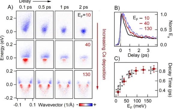
2A shows the differential signal obtained by subtract-ing the map acquired at negative to the one acquired at positive values of the pump-probe delay. Blue and red colors stand for photoexcited electrons and holes in the electronic system, respectively. These panels offer a vi-sual guide of the electronic cooling for three indicative densities (EF = 10, 40, 130 meV). A qualitative analysis
of the differential intensity maps provides clear evidence of the dimensionality crossover. Note that excited elec-trons are distributed in a broad area of reciprocal space when EF = 10 meV. This signal originates from many 3D
states with different values of the perpendicular wavevec-tor kz. Since these 3D states disperse along the z axis,
the excited electrons cover part of the projected band structure. In contrast, when EF = 130 meV the
differen-tial intensity is concentrated along a nearly free electron parabola that has no measurable dispersion in the z di-rection. From this map, we deduce that hot electrons become confined in the high doping regime.
Figure 2B plots the temporal evolution of the excess energy normalized to its maximal value. Initially, the ex-cited electrons experience a subpicosecond relaxation due to emission of LO phonon with small momentum trans-fer. After 1-2 ps, such subset of phonon modes enters in
equilibrium with hot electrons. The subsequent dynam-ics is dictated by anharmonic decay of the hot optical phonons in to lattice modes of lower energy. Here we are interested only in the relaxation at early delay, namely when LO phonons are still near to equilibrium conditions. As shown in Fig. 2B, the initial cooling time τ becomes twice slower at high carrier concentration. Measurements on two different cleaves confirm that τ is roughly 0.4 ps in the pristine surface, while it saturates to 0.8 ps upon in-creasing the concentration of absorbed Cs (see Fig. 2C). We estimate the cooling rate η of the electronic system as the average excess energy at 0.1 ps divided by cool-ing time τ . Figure 3A shows that this rate decreases by nearly one order of magnitude when moving from the classical to the quantum regime.
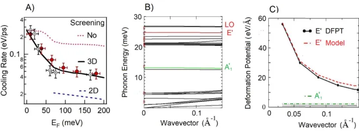
In order to simulate the cooling rate, we calculated the phonon spectrum by density functional perturbation theory (DFPT) (see Fig. 3B). We identify for each di-rection in wavevector space the polar and the non-polar branches. Since the excited electrons have small wavevec-tor, the phonon emission is limited to a wavevector trans-fer q < 0.2 1/˚A. The unscreened scattering with polar optical is long ranged and diverges for small wavevector transfer30. As a consequence, we expect LO emission
4
FIG. 2: A) Differential intensity maps obtained by subtracting the photoelectron intensity at negative delay from the pho-toelectron intensity at positive delay. The panels from left to right display data acquired at increasing delay time after photoexcitation. Top, middle and bottom columns correspond to an electron gas with Fermi energy EF = 10, 40, 130 meV.
B) Temporal evolution of the average excess energy Exin the electron gas with different Fermi Energy. The curves have been
normalized to the maximal Ex value for better comparison. C) Initial decay time of average excess energy versus the Fermi
energy. Filled and open symbols indicate the results of two independent set of measurements.
to be the largely dominant electron-phonon scattering mechanism. This is a general property of polar semicon-ductors, such as for example GaAs29. To illustrate this point, we show on Fig. 3C the strength of the electron-phonon matrix elements for all electron-phonon modes of ε-InSe. Figure 3C shows that the coupling of the E0 polar mode is in average more than 10 times larger than the one of the best coupled non-polar mode (the mode with A01
symmetry). The contribution of the polar coupling to the energy relaxation rate scales as coupling matrix el-ement squared, being at least 100 times larger than the A01 non-polar one. With respect to the other non-polar modes this ratio becomes even larger, so that the black curves in Fig. 3C collapse to values near to the ordinate axis. Figure 3C also show that the matrix elements of the polar E0 mode nearly follow the q dependence predicted by the Vogl’s model30. We make use of the this result to
extrapolate the polar phonon coupling that is calculated by ab initio DFPT on a denser grid of wavevectors, .
We simulate the the cooling rate η due to Fr¨ohlich interaction by calculating31as
η = (1 − f (Ex− ~Ωem))ΩemΓem (1)
−(1 − f (Ex+ ~Ωabs))ΩabsΓabs
Here, f is Fermi-Dirac distribution function which
de-pends on the electronic temperature Teand on the
chem-ical potential, Γem and Γabs are the total probabilities
for emission and absorption, while Ωem and Ωabs are
ef-fective LO phonon frequencies for emission and absorp-tion (see supplementary informaabsorp-tion for details about the calculations27). For each value of the Fermi energy E
F,
we extract the electronic temperature Tefrom the
exper-imental curve in Fig. 1D and derive the chemical poten-tial µ on the base of a free electron model32. The value of Γem and Γabs strongly depend on the electron-phonon
coupling strength of the polar modes. The non-polar modes would contribute to the cooling rate with an ex-tra term below 0.01 eV/ps and can be neglected with respect to the emission of LO optical phonons. First we consider the case of a 3D electron gas with unscreened Fr¨ohlich interaction. As already shown by our previous work on the pristine surface18, this approach provides an
estimated value of the cooling rate that is in agreement with tr-ARPES experiments. Upon increasing the doping level, a moderate decrease of the calculated η takes place at the crossover from a classical to a quantum statis-tic. Nonetheless, this unscreened coupling badly over-estimates the experimental behavior even at moderate carriers concentration (see red dotted curve in Fig. 3A).
Thomas-FIG. 3: A) Electronic cooling rate η as a function of Fermi energy. Filled and open symbols represent data from two independent set of measurements. The black solid, dashed blue and dotted red curves are the cooling rates calculated by an ab-initio model with 3D, 2D and no screening of the Fr¨ohlich interaction, respectively. B) Calculated phonon dispersion of ε-InSe in Γ − M direction of the Brillouin zone. Polar optical mode E0 is shown in red, while the acoustical A01 mode is shown in green. Red
squares at q = 0 stand for experimental from Ref.28. C) Calculated electron-phonon deformation potentials as a function of
the phonon wavevector q along the Γ − M direction. The initial electronic state is in the conduction band at k = (0, 0.11, 0)2π a.
For the polar mode, both the results of the DFPT (Black circles) and Vogl model (red dotted line) are shown.
Fermi screening. We expect these simulations to be ac-curate for the regime γ < 1, namely when hot electrons retain their 3D character. Surprisingly, the black line in Fig. 3A shows that the screened 3D interaction matches well the experimental data even in the case of a quasi-2DEG. This result needs to be carefully addressed, since a dimensionality crossover towards 2D states is observed in photoelectron intensity maps with γ > 1. In order to gain more insights, we compute the η expected in a strictly two dimensional system with 2D Fr¨ohlich coupling10and 2D dielectric screening11. The perfect confinement of the ideal system does cut off the divergence of the polar inter-action at small wavevector. Moreover, the electron-hole excitations that are responsible for the screening response acquire a higher density in the phase space (consider that in a strictly 1D system the collective excitations become so strong even the Fermi liquid picture breaks down). As a consequence, the η of a strictly 2D model drops dra-matically already a small doping level. It is clear from the dashed blue line of Fig. 3A that such model grossly underestimates the experimental cooling rate. The dif-ference between the 2D model and experimental data is ascribed to a remote coupling between the quasi-2DEG and 3D phonons. The exact mechanism is still not iden-tified. It could be an energy transfer mediated by sur-face plasmons-polaritons or any other channel that cou-ples the confined electrons with LO modes that are not strictly two dimensional. An accurate simulation of such remote interaction would be a challenging task which is
beyond the scope of the present work. However, Fig. 3A shows that a 3D model with Thomas Fermi screening al-ready reproduces remarkably well the experimental data. In conclusion, hot electrons in quasi-2DEGs display a remote coupling to polar optical phonons persisting up to high electronic density. The accurate modeling of such in-teraction should include the wavefunctions of confined 2D electrons, dynamical screening effects, surface plasmons polaritons and interface phonons. Nonetheless, the static screening of bulk phonons by 3D electrons can quanti-tatively reproduce the experimental cooling rate. This finding highlights that electrons in accumulation layers or 2D conductors at the interface with a polar medium experience 3D dissipation channels. The outcome is of high relevance for the carriers mobility in FET devices with high κ dielectric gates, van der Waals heterostru-tures and 2DEGs at the interface between oxides.
We acknowledge enlightening discussions with Matteo Calandra and Valerie Veniard. Many thanks to the Ecole Polytechnique for funding under the project ECOGAN, the Chaire Energie Durable. Financial support has been given by the DGA project ITEHR (No. 2018 60 0074) and by the EU/FP7 program under the contract Go Fast (Grant No. 280555). Computer time has been granted by the national centers GENCI-CINES and GENCI-TGCC (Project 2210), and by Ecole Polytechnique through the LLR-LSI project. Computational results have been ob-tained via the QUANTUM ESPRESSO code34.
1 K. V. Klitzing, G. Dorda and M.Pepper, Phys. Rev. Lett.
45, 494 (1980).
6 Nat. Mater. 6, 810 (2007).
3 B. Jeckelmann and B. Jeanneret, Rep. Prog. Phys. 64,
1603 (2001).
4
E. Lesne, Y. Fu, S. Oyarzun, J. C. Rojas-S´anchez, D. C. Vaz, H. Naganuma, G. Sicoli, J.-P. Attan´e, M. Jamet, E. Jacquet, J.-M. George, and A. Barth´el´emy, and H. Jaffr`es, A. Fert, M. Bibes and L. Vila, Nat. Mater. 15, 1261 (2016).
5
A. Liu, R. Jones, L. Liao, D. Samara-Rubio, D. Rubin, O. Cohen, R. Nicolaescu and M. Paniccia, Nature 427, 615 (2004).
6
M. Houssa, High κ dielectrics (Institute of Physics Pub-lishing, Bristol and Philadelphia, 2004).
7
J. A. del Alamo, Nature 479, 317 (2011).
8
A. Ohtomo and H. Y. Hwang, Nature 427, 423 (2004).
9 B. Radisavljevic, A. Radenovic, J. Brivio, V. Giacometti
and A. Kis, Nat. Nanotechnol. 6, 147 (2011).
10
T. Sohier, M. Calandra and F. Mauri, Phys. Rev. B 94, 085415 (2016).
11 F. Stern, Phys. Rev. Lett. 18, 546 (1967). 12
J.-H. Chen, C. Jang, S. Xiao, M. Ishigami and M. S. Fuhrer, Nat. Nanotechnol. 3, 206 (2008).
13 M. V. Fischetti, D. A. Neumayer, and E. A. Cartier, J.
Appl. Phys. 90, 4587 (2001).
14
J. Kim, S. S. Baik, S. H. Ryu,Y. Sohn, S. Park, B.-G. Park, J. Denlinger, Y. Yi, H. J. Choi and K. S. Kim, Science 349, 723 (2015).
15
Z. Chen, J. Biscaras, and A. Shukla, Nanoscale 7, 5981 (2015).
16
D. A. Bandurin, A. V. Tyurnina, G. L. Yu, A. Mishchenko, V. Z´olyomi, S. V. Morozov, R. K. Kumar, V. Gorbachev, Z. R. Kudrynskyi, S. Pezzini, Z. D. Kovalyuk, U. Zeitler, K. S. Novoselov, A. Patan`e, L. Eaves, I. V. Grigorieva, V. I. Fal’ko, A. K. Geim and Y. Cao, Nat. Nanotechnol. 12, 223 (2017).
17 Z. Zhang, Z. Chen, M. Bouaziz, C. Giorgetti, H. Yi, J.
Avila, B. Tian, A. Shukla, L. Perfetti, D. Fan, Y. Li and A. Bendounan, ACS Nano 13, 13486 (2019).
18 Z. Chen, C. Giorgetti, J. Sjakste, R. Cabouat, V. V´eniard,
Z. Zhang, A. Taleb-Ibrahimi, E. Papalazarou, M. Marsi, A. Shukla, J. Peretti and L. Perfetti, Phys. Rev. B 97, 241201(R) (2018).
19
S. J. Magorrian, V. Z´olyomi and V. I. Fal’ko, Phys. Rev. B 94, 245431 (2016).
20 W. Meevasana, P. D. C. King, R. H. He, S. K. Mo, M.
Hashimoto, A. Tamai, P. Songsiriritthigul, F. Baumberger
and Z. X. Shen, Nat. Mater. 10, 114 (2011).
21 D. Hsieh, Y. Xia, D. Qian, L. Wray, J. H. Dil, F. Meier, J.
Osterwalder, L. Patthey, J. G. Checkelsky, N. P. Ong, A. V. Fedorov, H. Lin, A. Bansil, D. Grauer, Y. S. Hor, R. J. Cava and M. Z. Hasan, Nature 460, 1101 (2009).
22 E. Papalazarou, L. Khalil, M. Caputo, L. Perfetti, N.
Nil-foroushan, H. Deng, Z. Chen, S. Zhao, A. Taleb-Ibrahimi, M. Konczykowski, A. Hruban, A. Wolo´s, A. Materna, L. Krusin-Elbaum and M. Marsi Phys. Rev. Mater. 2, 104202 (2018).
23
Z. Chen, J. Dong, E. Papalazarou, M. Marsi, C. Giorgetti, Z. Zhang, B. Tian, J.-P. Rueff, A. Taleb-Ibrahimi and L. Perfetti, Nano Lett. 19, 488 (2019).
24
Z. Chen, Min-i Lee, Z. Zhang, H. Diab, D. Garrot, F. L´ed´ee, P. Fertey, E. Papalazarou, M. Marsi, C. Ponseca, E. Deleporte, A. Tejeda and L. Perfetti Phys. Rev. Mater. 1, 045402 (2017).
25 A. Chevy, J. Cryst. Growth 67, 119 (1984).
26 J. Faure, J. Mauchain, E. Papalazarou, W. Yan, J. Pinon,
M. Marsi and L. Perfetti, Rev. Sci. Instrum. 83, 043109, (2012).
27 The supplementary information contain additional
exper-imental data of surface photovoltage and a discussion of the band bending before and after Cs deposition, describe the coupling of polar modes, the models employed to cal-culate the electron-phonon matrix elements, the dielectric screening and the cooling rate.
28 Indium selenide (InSe) phonon wavenumbers: Datasheet
from Landolt-B¨ornstein - Group III Condensed Matter Volume 41C: Non-Tetrahedrally Bonded Elements and Bi-nary Compounds, ed. O. Madelung, U. R¨ossler, M. Schulz, (1998).
29
J. Sjakste, K. Tanimura, G. Barbarino, L. Perfetti and N. Vast, J. Phys. Condens. Matter 30, 353001 (2018).
30 P. Vogl, Phys. Rev. B 13, 694 (1976). 31
P. Allen, Phys. Rev. Lett. 59, 1460 (1987).
32
S. Panda and B. K. Panda, J. Phys. Condens. Matter 20, 485201 (2008).
33
J. Sjakste, N. Vast, M. Calandra and F. Mauri, Phys. Rev. B 92, 054307 (2015).
34 P. Giannozzi, O. Andreussi, T. Brumme, O. Bunau, M. B.
Nardelli, M. Calandra, R. Car, C. Cavazzoni, D. Ceresoli, M. Cococcioni, et al., J. Phys. Condens. Matter 29, 465901 (2017).