Peter Kr. Petrova)
Imperial College, London SW7 2AZ, United Kingdom Vaijayanti R. Palkar
Tata Institute of Fundamental Research, Mumbai 400005, India Alexander K Tagantsev
Ceramics Laboratory, Swiss Federal Institute of Technology (EPFL), Lausanne CH-1015, Switzerland Hsin-I Chien
London South Bank University, London SE1 0AA, United Kingdom K. Prashanthi
Indian Institute of Technology Bombay, Mumbai 400076, India Anna-Karin Axelsson
Imperial College, London SW7 2AZ, United Kingdom S. Bhattacharya
Tata Institute of Fundamental Research, Mumbai 400005, India Neil McN Alford
Imperial College, London SW7 2AZ, United Kingdom
(Received 3 January 2007; accepted 22 May 2007)
The dielectric response of La- and Dy- doped BiFeO3thin films at microwave
frequencies (up to 12 GHz) has been monitored as a function of frequency, direct current (dc) electric field, and magnetic field in a temperature range from 25 to 300 °C. Both the real and imaginary parts of the response have been found to be non-monotonic (oscillating) functions of measuring frequency. These oscillations are not particularly sensitive to a dc electric field; however, they are substantially
dampened by a magnetic field. The same effect has been observed when the volume of the characterized sample is increased. This phenomenon is attributed to the presence of a limited number of structural features with a resonance type response. The exact origin of these features is unknown at present. Leakage current investigations were performed on the whole set of films. The films were highly resistive with low leakage current, thereby giving us confidence in the microwave measurements. These typically revealed ‘N’-type I-V characteristics.
I. INTRODUCTION
Multiferroic (MF) materials are those in which more than one ferroic order (magnetic, electric, elastic) co-exists and is coupled.1
The possibility of including extra functionality with a device makes MF materials very attractive for application in microwave technology. How-ever, there are no (or very few) papers reporting the properties of MF materials at frequencies higher than a few megahertz. The main reason for the lack of published high-frequency [radio frequency (rf) and microwave]
measurement data is the high leakage current in these materials and especially in samples of thin films.
BiFeO3 (BFO) is one of the very few single-phase
multiferroic materials and is the subject of increased sci-entific interest.2–4
The challenges with BiFeO3 (BFO)
arise from its large leakage current4
and from the fact that at room temperatures bulk BFO is ferroelectric and an-tiferromagnetic.3Doping of BFO with Dy and La helps in the stabilization of the perovskite phase and in the reduction of leakage current. The idea of La doping is known to restrain the formation of a non-ferroelectric second phase and to stabilize the perovskite phase. Also, as observed in Ref. 4, doping BiFeO3 films with La
gradually changes the film structure from a monoclini-cally tilted state to a nontilted tetragonal like state. The a)
Address all correspondence to this author. e-mail: [email protected]
spatially inhomogeneous spin-modulated incommensu-rate structure of BFO gradually disappears with increas-ing concentration of La, leadincreas-ing to the structural phase transition at x < 0.2 in Bi1−xLaxFeO3, which corresponds
to the change in the unit-cell symmetry from R3c to C3v. The authors have also shown increase in magnetization and fatigue-free ferroelectric switching characteristics with La doping in BiFeO3. Therefore, we studied film
characteristics of Dy-modified BiFeO3 thin films with
and without La doping.
In this work, we present the results of a comprehensive study on the dielectric response of doped BFO thin films in microwave-frequency range as well as the effect of applied direct-current (dc) electric and magnetic fields. Also reported are the current–voltage characteristics of the samples.
II. EXPERIMENTAL
Thin films of Bi0.7Dy0.3FeO3and Bi0.6La0.1Dy0.3FeO3
were deposited on single-crystal LaAlO3and MgO
sub-strates using pulsed laser deposition (PLD). A PM882 GSI-Lumonics (Kanata, Ontario, Canada), 248 KrF ex-cimer laser was used for the ablation process. For the deposition, stoichiometric targets of Bi0.7Dy0.3FeO3and
Bi0.6La0.1Dy0.3FeO3, synthesized by a partial
cotation route, were used. NaOH was used as the precipi-tating agent. The precipitate was filtered out, washed, and then dried under an infrared lamp. The dried powders were pulverized and calcined at 600 °C for 1 h to obtain the reacted material. The calcined powder was pressed to form a pellet and sintered at 800 °C for 2 h to obtain a dense target for laser ablation. Pulsed laser ablation con-ditions were optimized to achieve phase-pure, granular, homogeneous, and insulating thin films of both the com-pounds. The typical film thickness was∼220 nm.
The crystal structure of the samples was investigated by x-ray diffraction (XRD) using a PANalytical X’Pert MRD system (Almelo, The Netherlands) with Cu K␣ radiation. Measurements were performed using an X’Celerator diffractometer with monochromator at-tached. The sample microstructure was examined on Hi-tachi 4500 field-emission SEM (Tokyo, Japan).
For electrical testing planar capacitors, structures with 3 and 5m gap-size were patterned on the film surface; 0.5-m-thick Au/Ti electrodes were formed using E-beam evaporation followed by photolithography and ion-milling performed on an Oxford Applied Research OAR–IM150 system (Witney, Oxfordshire, UK).
Electrical measurements were performed on a Signa-tone probe station (Gilroy, CA). The current–voltage characteristics were measured using an Agilent B1500A semiconductor device analyzer (Santa Clara, CA). An Agilent 4287A RF LCR meter was used for direct meas-urement of the sample capacitance and Q-factor (up to
3 GHz). At higher frequencies (up to 12 GHz), these values were evaluated from the Agilent 8722 ES VNA measured S11-parameter using the procedure described in Ref. 5. To examine the effect of dc electric field on the dielectric response of the material, a dc bias up to 100 V was applied to the samples via a Picoprobe bias-tee (Naples, FL). A home-made temperature stage (accuracy ±1 °C) was used for temperature measurements up to 300 °C, while a 0.15T permanent magnet was used for dielectric measurements under a magnetic field.
III. RESULTS AND DISCUSSION
In this work, we refer to Bi0.7Dy0.3FeO3 films on
LaAlO3 and MgO substrates as DL and DM,
respec-tively, and Bi0.6La0.1Dy0.3FeO3 films on LaAlO3 and
MgO substrates as DLL and DLM, respectively. These abbreviations will be used further in this paper.
A. Crystal structure
XRD analysis showed that all samples have good crys-tallinity. Films grown on LaAlO3 were single-faced
(010) oriented [Fig. 1(a)], while (104) and (110) peaks were observed as well on the films grown on MgO sub-strates [Fig. 1(b)]. Lattice spacings d/n(0k0) evaluated from the position of the observed peaks were 3.888 Å for
FIG. 1. XRD patterns of Dy- and La-doped BiFeO3thin films grown on (a) LaAlO3substrate and (b) MgO substrate. (Au peaks are from the electrodes, formed to enable electrical measurements.)
the films on the LAO substrate and 3.885 Å for the films on MgO substrate.
Scanning electron microscopy revealed that all films have nano-scale granular structure. Also observed were granules randomly distributed on the sample’ surface [Fig. 2(a)].
B. I-V measurements
A typical I-V characteristic of the materials is pre-sented in Fig. 3. In addition to the fact that the conduc-tivity in the samples is low enough to allow them to be measured at high frequency, this investigation revealed some unexpected and very interesting results.
Note that Ohm’s law does not hold for these samples. For the sake of comparison, let us divide the I-V curve into three regions, as shown in Fig. 3, and estimate the conductivity in these regions. The conductivity in region 1 is∼1 × 10⁻⁴⍀−1cm−1, a value typical for the pure BFO. In region 2, there is negative resistance. In region 3, the
system reduces its conductivity by 2–3 orders of magni-tude compared with pure BFO. It is important to note that the values of the samples’ conductivity varied from sample to sample (even those patterned on the same sub-strate); however, ‘N’-type I-V was observed in about 80% of the samples. At present, we do not have a good explanation for this behavior, and work is in progress to find a convincing reason for the observed phenomenon. C. Capacitance and the Q-factor
versus frequency
Figure 4(a) shows the typical behavior of the capaci-tance and the Q-factor at microwave frequencies. We observe many local peaks (oscillations) in both charac-teristics, which occur in the measurements of all samples [see Fig. 4(b)]. The non-monotonic variation of the ca-pacitance with frequency strongly suggests that the di-electric response is controlled by the coupling of the electric field with structural features exhibiting the reso-nance rather than relaxation type response, which is rare in the microwave-frequency range. A remarkable feature of these oscillations is that these can be “damped” by increasing the distance between the electrodes of the measuring capacitor (see Fig. 5). Such behavior can be attributed to a small number of resonating species in the gap of the planar capacitor: the oscillations are smeared or damped more in the case of a wider gap, which con-tains a larger number of the features. Thus, it seems that we are dealing with a situation reminiscent of the clas-sical mesoscopic effect,6 where not the average of the spatial distribution of impurities, but rather the inhomo-geneity of their distribution governs the properties of the materials and results in fluctuations of their conductance. We note that only the capacitance and Q-factor are presented. This eliminates the uncertainty introduced by the dielectric permittivity–dielectric loss tangent evalua-tion procedures. The measurement uncertainty of the measured capacitance and Q-factor is less than 5%,7 al-lowing us to discuss the observed oscillations with con-fidence. When dielectric permittivity–dielectric loss FIG. 2. SEM images of Dy- and La-doped BiFeO3thin films showing
(a) the nano-scale granular structure of the films and (b) the observed granules randomly distributed on the sample surface.
tangent evaluation procedures are used, the measurement uncertainty is further increased to 20–30% (due-to the model limitations and effect of the electrodes and inter-face layers),5,8,9 which makes the above discussion less credible. Thus, we are confident that the observed oscil-lation in capacitance and Q factor is a true electrical effect. The error introduced in the evaluation of relative permittivity (film thickness, electrode dimensions, etc.) makes us less certain of these quantities. Nevertheless, taking this into account, we estimate that in the 0.1– 12 GHz frequency range, the dielectric permittivities for films on LAO and MgO substrates, were about 300 and 200, respectively, while the loss tangent, calculated as 1/Q, was between 0.01 and 0.1.
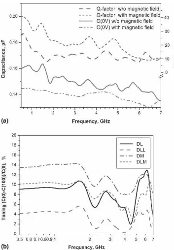
D. Effect of dc electric field
Tuning of the capacitance (calculated as {[C(0V) − C(100V)]/C(0V)} × 100%) by 2–4% was measured un-der an electric field of 200kV/cm (see Fig. 6). Samples on MgO substrates exhibited higher tuneability, which might be related to a higher residual strain in the films as FIG. 5. Frequency dispersion of the capacitance measured for
capaci-tors with 3- and 5-m gap size, at 0 V, 25 °C.
FIG. 6. Effect of the electric field of dielectric response of the Dy- and La-doped BiFeO3thin film: (a) typical behavior of the capacitance and Q-factor versus frequency at 0 and 100 V and (b) tuning versus frequency. FIG. 4. Frequency dispersion of the dielectric properties of Dy- and
La-doped BiFeO3thin films measured at 0 V, 25 °C: (a) typical be-havior of the capacitance and Q-factor versus frequency and (b) fre-quency dispersion of the capacitance.
a consequence of the lattice mismatch. The presence of La further enhances the tuneability (on average) by a factor of two. It seems that the mechanism of tuneability is different from that active in traditional ferroelectrics such as (Ba,Sr)TiO3; in our materials, the reduction of
permittivity (with increasing frequency) is accompanied with an appreciable increase of the tuneability, a trend opposite that observed in typical ferroelectric systems.10 E. Effect of permanent magnetic field
As one can see in Fig. 7, the effect of the magnetic field on the dielectric response was larger for the samples de-posited on MgO substrates. However, now the La doping causes a decrease in the response. The Q-factor however, increases when a magnetic field is applied. Remarkably, the application of the magnetic field leads to an appreciable smearing of the oscillations in the C( f ) curves, an effect similar to that caused by increasing the capacitor gap. F. Effect of elevated temperature
Elevated temperature seems not to affect the oscilla-tion in the C( f ) curves. They exist [see Fig. 8(a)] at
tem-peratures up to 300 °C, the maximum temperature we could apply. The temperature dependence of the capaci-tance is very weak, as seen from Fig. 8(b).
IV. CONCLUSIONS
The microwave dielectric response and the conductiv-ity of La- and Dy-doped BiFeO3thin films was examined
under dc electric and magnetic fields and in a tempera-ture range from 25 to 300 °C . We observed strong os-cillations in the C( f ) characteristic, which we interpreted as a manifestation of a small number of structural fea-tures with a dielectric resonance. Further evidence sup-porting this speculation was a damping of the C( f ) char-acteristic when the capacitor gap-size was increased; i.e., the number of features involved in the response was in-creased. These resonating features are rather sensitive to the magnetic field and less sensitive to the dc electric field. One region in the I-V characteristic of the samples shows a negative differential resistance. Finally, doping with Dy and La leads to a leakage reduction. However the presence of La weakened the magnetic response of the system.
The novel phenomena revealed in this study are true FIG. 7. Effect of permanent magnetic field on the dielectric response
of the Dy- and La-doped BiFeO3thin films: (a) typical behavior of the capacitance and Q-factor versus frequency at a magnetic field of 0 and 0.15 T and (b) magnetic tuning versus frequency.
FIG. 8. Dielectric response of the Dy- and La-doped BiFeO3thin films at elevated temperature: (a) typical behavior of the capacitance versus frequency as a function of temperature and (b) capacitance versus temperature measured at 1.25 GHz.
electrical effects, even though at present (because of un-certainty introduced by the evaluation procedure) we are unable to state the exact values of thin films’ dielectric permittivity and loss tangent with confidence. This re-quires the use of other measurement techniques and evaluation procedures with lower uncertainty level. Nev-ertheless, the observed results show the potential appli-cability of multiferroic materials at rf and microwave frequencies.
REFERENCES
1. G.A. Smolenski: Ferroelectromagnets. Sov. Phys. Usp. 25, 475 (1982).
2. V.R. Palkar, J. John, and R. Pinto: Observation of saturated po-larization and dielectric anomaly in magnetoelectric BiFeO3thin films. Appl. Phys. Lett. 80, 1628 (2002).
3. S. Shetty, V.R. Palkar, and R. Pinto: BiFeO3thin films: Novel effects. PRAMANA-J. Phys. 58, 1027 (2002).
4. D. Lee, M.G. Kim, S. Ryu, H.M. Jang, and S.G. Lee: Epitaxially grown La-modified BiFeO3magnetoferroelectric thin films. Appl. Phys. Lett. 86, 222903 (2005).
5. P.K. Petrov, N.McN. Alford, and S. Gevorgyan: Techniques for microwave measurements of ferroelectric thin films and their as-sociated error and limitations. Meas. Sci. Technol. 16, 583 (2005). 6. B. Spivak, F. Zhou, and M.T. Beal Monod: Mesoscopic mecha-nisms of the photovoltaic effect and microwave absorption in granular metals. Phys. Rev. B: Condens. Matter 51, 13226 (1995). 7. Agilent Technologies 4287A RF-LCR Meter User’s Guide, Part No. 04287-90502 (Agilent Technologies Inc., Santa Clara, CA, 2003).
8. O.G. Vendik, S.P. Zubko, and M.A. Nikol’ski: Modeling and calculation of the capacitance of a planar capacitor containing a ferroelectric thin film. Tech. Phys. 44, 349 (1999).
9. P.K. Petrov, Y. Pan, and N.McN. Alford: Dielectric constant and loss tangent of thin ferroelectric films at microwave frequencies— How accurately can we evaluate them? Integrated Ferroelectrics (in press).
10. A.K. Tagantsev, V.O. Sherman, K.F. Astafiev, J. Venkatesh, and N. Setter: Ferroelectric materials for microwave tunable applica-tions. J. Electroceram. 11, 5 (2003).