HAL Id: tel-01216463
https://tel.archives-ouvertes.fr/tel-01216463
Submitted on 16 Oct 2015HAL is a multi-disciplinary open access archive for the deposit and dissemination of sci-entific research documents, whether they are pub-lished or not. The documents may come from
L’archive ouverte pluridisciplinaire HAL, est destinée au dépôt et à la diffusion de documents scientifiques de niveau recherche, publiés ou non, émanant des établissements d’enseignement et de
Electrical characterization of interface properties in
nano-scaled MOSFET devices based on low-frequency
fluctuations
Masahiro Koyama
To cite this version:
Masahiro Koyama. Electrical characterization of interface properties in nano-scaled MOSFET de-vices based on low-frequency fluctuations. Micro and nanotechnologies/Microelectronics. Université Grenoble Alpes, 2015. English. �NNT : 2015GREAT036�. �tel-01216463�
THÈSE
Pour obtenir le grade de
DOCTEUR DE L’UNIVERSITÉ DE GRENOBLE
Spécialité : Nano Électronique et Nano Technologies (NENT) Arrêté ministériel : 7 août 2006Présentée par
Masahiro KOYAMA
Thèse dirigée par Gérard GHIBAUDO et codirigée par Mikaël CASSÉ
préparée au sein du Laboratoire CEA-LETI dans l'École Doctorale EEATS
Caractérisation électrique des
propriétés d'interface dans les
MOSFET nanométriques par des
mesures de bruit basse
fréquence
Thèse soutenue publiquement le 26 mars 2015 devant le jury composé de :
M. Abdelkader SOUIFI
PR, INSA de Lyon, Président
M. Cor CLAEYS
Professeur étranger, Université Catholique de Leuven, Rapporteur
Mme. Nathalie MALBERT
PR, Université de Bordeaux, Rapporteur
M. Hiroshi IWAI
Professeur étranger, Tokyo Institute of Technology, Examinateur
Dissertation for the degree of Doctor of Philosophy
Electrical characterization of interface properties in
nano-scaled MOSFET devices based on low-frequency
fluctuations
By Masahiro KOYAMA
CEA-LETI, MINATEC Campus, 17 rue des Martyrs, 38054 Grenoble, France
January 2015
Supervisor: Gérard GHIBAUDO
IMEP-LAHC, Grenoble INP-MINATEC, 3 Parvis Louis Néel, 38016 Grenoble, France
Co-supervisor: Mikaël CASSÉ
Résumé
Dans cette thèse, les propriétés électriques de transistors à nanofils de silicium liéesà l’interface oxyde de grille/canal ont été étudiées par le biais de mesures de bruit basse fréquence (bruit 1/f) et de transport dans le canal. Ces transistors nanofils dont les dimensions ont été réduites jusqu’à quelques nanomètres pour la section, représentent une alternative sérieuse pour les futurs nœuds technologiques CMOS. Cependant, la qualité de l’interface oxyde de grille/canal pose question pour transistors dont l’architecture s’étend dans les 3 dimensions, en raison du fort rapport surface/volume inhérent à ces transistors, des différentes orientations cristallographiques de ces interfaces, ou encore des matériaux contraints utilisés pour améliorer les performances électriques. La compréhension des liens entre les propriétés de transport des porteurs dans le canal, qui garantissent en grande partie les performances électriques des transistors, et la qualité de l’interface avec l’oxyde de grille est fond primordiale pour optimiser les transistors nanofils. Les mesures de bruit, associées à l’étude du transport dans le canal, sont un outil puissant et adapté à ces dispositifs tridimensionnels, sans être limité par la taille ultra-réduite des transistors nanofils.
Les transistors nanofils étudiés ont été fabriqués à partir de substrats minces SOI, et intègrent un empilement de grille HfSiON/TiN, qui permet de réduire les dimensions tout en conservant les mêmes propriétés électrostatiques. Pour gagner en performances, des contraintes mécaniques ont été introduites dans le canal en silicium : en tension pour les NMOS, par le biais de substrat contraint (sSOI), et en compression pour les PMOS. Un canal en compression uni-axiale peut être obtenu par l’intégration de source/drain en SiGe et/ou par l’utilisation de couches contraintes de type CESL. Des transistors à canal SiGe sur isolant en compression ont également été fabriqués et étudiés.
Les caractéristiques électriques des divers transistors nanofils (courbes Id-Vg, compromis Ion-Ioff, mobilité des porteurs) démontrent l’excellent contrôle électrostatique dû à l’architecture 3D, ainsi que l’efficacité de l’ingénierie de contraintes dans les nanofils jusqu’à de faibles longueurs de grilles (~17nm).
Des mesures de bruit basse fréquence ont été réalisées sur ces mêmes dispositifs et analysées en fonction des paramètres géométriques de l’architecture nanofils (largeur W,
forme de la section, longueur de grille L), et des diverses variantes technologiques. Nous avons démontré que le bruit 1/f dans les transistors nanofils peut être décrit par le modèle de fluctuations du nombre de porteurs (CNF) corrélées aux fluctuations de mobilité (CMF). Le bruit associé aux régions S/D a pu également être intégré dans ce modèle en ajoutant une contribution, en particulier pour les PMOS.
Alors que les différentes variantes technologiques ont peu d’effet sur le bruit 1/f, les variations de géométrie en L et W changent la composante de bruit liée aux fluctuations du nombre de porteurs (CNF) de manière inversement proportionnelle à la surface totale (~1/WL). Cette augmentation du bruit est le reflet du transport qui se produit à proximité des interfaces avec l’oxyde. Les différentes orientations des interfaces supérieures et latérales (110) ou (100) présentent la même quantité de pièges d’interface (extrait à partir des mesures de bruit 1/f, en séparant les contributions des différentes faces du nanofil) bien qu’ayant une rugosité différente essentiellement liée au process. En revanche la composante CMF n’est pas altérée par la réduction des dimensions contrairement à la mobilité des porteurs qui décroit fortement avec L.
Finalement, les mesures de bruit 1/f ont été comparées aux spécifications ITRS 2013 pour les transistors multi-grilles en vue des futurs nœuds technologiques de la logique CMOS, et démontrent que nos transistors nanofils satisfont les exigences en la matière.
Mots-clés
MOSFET, Nanofils, Bruit basse fréquence, CaractérisationAbstract
In this thesis, electrical properties of gate oxide/channel interface in ultra-scaled nanowire (NW) MOSFETs were experimentally investigated by carrier transport and low-frequency noise (LFN) characterizations. NW FETs, which have aggressively downscaled cross-section of the body, are strong candidates for near future CMOS node. However, the interface quality could be a critical issue due to the large surface/volume ratio, the multiple surface orientations, and additional strain technology to enhance the performance. Understanding of carrier transport and channel interface quality in NW FETs with advanced high-k/metal gate is thus particularly important. LFN provides deep insights into the interface properties of MOSFET without lower limit of required channel size. LFN measurement thus can be a powerful technique for ultra-scaled NW FETs. Also, fitting mobility (such as low-field mobility) extraction by Y-function method is an efficient method.Omega-gate NW FETs were fabricated from FD-SOI substrates, and with Hf-based high-k/metal gate (HfSiON/TiN), reducing detrimental effects by device downscaling. In addition, strain technologies to the channel were additively processed. Tensile strained-SOI substrate was used for NMOS, whereas compressive stressors were used for PMOS devices. Strained Si channel for PMOS was processed by raised SiGe S/D and CESL formations. Strained SiGe channel (SGOI) was also fabricated for further high-performance PMOS FETs.
Firstly, the most common Id-Vg was characterized in single-channel NW FETs as the basic performance. Reference SOI NWs provided the excellent static control down to short channel of 17nm. Stressors dramatically enhanced on-current owing to a modification of channel energy-band structure. Then, extracted low-field mobility in NWs also showed large improvement of the performance by stressors. The mobility extraction effectively evaluated FET performance even for ultra-scaled NWs.
Next, LFN investigated for various technological and architectural parameters. Carrier number fluctuations with correlated mobility fluctuations (CNF+CMF) model described 1/f noise in all our FETs down to the shortest NWs. Drain current noise behavior was basically similar in both N- and PMOS FETs regardless of technological splits. Larger 1/f noise stemming from S/D regions in PMOS FETs was perfectly
interpreted by the CNF+CMF model completed with Rsd fluctuations. This observation highlighted an advantage of SGOI NW with the lowest level of S/D region noise.
Geometrical variations altered the CNF component with simple impact of device scaling (reciprocal to both Wtot and Lg). No large impact of surface orientation difference between the channel (100) top and (110) side-walls in [110]-oriented NWs was observed. Scaling regularity with both Wtot and Lg, without much quantum effect, could be attributed to the use of HfSiON/TiN gate and carrier transport occurring mostly near top and side-wall surfaces even in NW geometry. Meanwhile, the CMF factor was not altered by decreasing dimensions, while the mobility strongly depends on the impact.
Extracted oxide trap density was roughly steady with scaling, structure, and technological parameter impacts. Simple separation method of the contributions between channel top surface and side-walls was demonstrated in order to evaluate the difference. It revealed that oxide quality on (100) top and (110) side-walls was roughly comparable in all the [110]-devices. The density values lie in similar order as the recent reports. An excellent quality of the interface with HfSiON/TiN gate was thus sustained for all our technological and geometrical splits.
Finally, our NWs fulfilled 1/f LFN requirements stated in the ITRS 2013 for future MG CMOS logic node. Consequently, we concluded that appropriate strain technologies powerfully improve both carrier transport and LFN property for future CMOS circuits consisting of NW FETs, without any large concern about the interface quality.
Keywords
MOSFET, Nanowire, Low-frequency noise, CharacterizationAcknowledgments
I would like to thank profoundly my supervisors, Professor Gérard Ghibaudo at IMEP-LAHC and Dr. Mikaël Cassé at CEA LETI, for their passionate tutelage, encouragement, and thoughtful supports not only throughout my study but also for life.
I am also deeply grateful to Dr. Simon Deleonibus, Dr. Gilles Reimbold, Dr. Sylvain Barraud, Dr. Rémi Coquand, and Ms. Estelle Brague at CEA LETI for their fruitful collaboration and great help. All researchers and engineers at CEA LETI and IMEP-LAHC with whom I have worked are also gratefully acknowledged. The life in Grenobele, France, was exciting and beautiful experiences. I really appreciate and will never forget the wonderful days, friendship with a lot of people, and their kindness.
And I would like to thank Professor Hiroshi Iwai, Professor Takeo Hattori, Professor Kenji Natori, Professor Yoshinori Kataoka, Professor Akira Nishiyama, Professor Nobuyuki Sugii, Professor Kazuo Tsutsui, Professor Hitoshi Wakabayashi, and Professor Kuniyuki Kakushima at Tokyo Institute of Technology for their worthful advisements. I am also thankful to research colleagues of Iwai-Kakushima laboratory for their friendship, and to secretaries of the laboratory, Ms. Akiko Matsumoto and Ms. Masako Nishizawa, for their kind assistance.
This work was partially carried out in the frame of the STMicroelectronics/IBM/CEA-LETI joint program and by the French Public Authorities through NANO 2017 program.
Acknowledgments
To my family
for everything to date
Table of Contents
Résumé & Abstract 2
Acknowledgements 6
List of Tables 12
List of Figures 13
List of Symbols, Acronyms, and Abbreviations 21
Chapter 1. Introduction 27
1.1 General Context 28
1.2.1 MOSFET downscaling -Moore's law- 28
1.2.2 Power consumption of CMOS logic circuits 30
1.2.3 End of scaling era? 33
1.2 Purposes and scopes of this work 37
1.3 References 44
Chapter 2. Nanowire MOSFETs 50
2.1 Introduction to MOSFETs for the next technological nodes 51
2.1.1 Fundamentals of MOSFET 51
2.1.1.1 MOSFET as a switch 2.1.1.2 Threshold voltage 2.1.1.3 Subthreshold swing 2.1.1.4 Short-channel effects 2.1.2 Key concepts for advanced MOSFET 58
2.1.2.1 FD-SOI devices 2.1.2.2 Multi-gate devices 2.1.2.3 High- dielectric/metal gate system 2.1.2.4 Strain technology 2.2 Our nanowire devices 73
Table of Contents
2.2.2 Key device parameters 74
2.2.2.1 Architectural splits 2.2.2.2 High-/metal gate stack 2.2.2.3 Additional H2 anneal
2.2.2.4 Tensile strained-SOI (sSOI) devices for NMOS
2.2.2.5 Compressively strained SiGe-on-insulator (SGOI) for PMOS 2.2.2.6 Additional strain sources: SiGe source/drain and CESL
2.2.3 Descriptions of all the device parameters 81
2.3 References 84
Chapter 3. Carrier transport characterizations 95
3.1 Methodology 96 3.1.1 Id-Vg measurement 96 3.1.2 Cgc-Vg measurement 97 3.1.3 Mobility extraction 98 3.1.3.1 Effective mobility 3.1.3.2 Low-field mobility 3.2 Experimental results 101 3.2.1 Id-Vg characteristics 101 3.2.1.1 Threshold voltage
3.2.1.2 Drain induced barrier lowering
3.2.1.3 Subthreshold swing
3.2.1.4 Challenge of ION enhancement
3.2.2 Temperature dependent Effective mobility 114 3.2.2.1 Extraction of contributions of side-wall and top surfaces 3.2.2.2 Tri-gate vs. omega-gate
3.2.2.3 Impact of tensile strain
3.2.3 Low-field mobility 125
3.2.3.1 Extracted low-field mobility 3.2.3.2 Mobility degradation factor
Table of Contents
Chapter 4. Low-frequency noise characterizations 137
4.1 Fundamentals 138
4.1.1 Introduction to main noise sources 138
4.1.1.1 Thermal noise
4.1.1.2 Shot noise
4.1.1.3 Generation-recombination (g-r) noise 4.1.1.4 Random-telegraph-signal (RTS) noise
4.1.1.5 1/f noise
4.1.2 Low-frequency noise in MOSFET 145 4.1.2.1 LFN measurements as a diagnostic tool
4.1.2.2 Hooge empirical model - Mobility fluctuations 4.1.2.3 McWhorter model - Carrier number fluctuations
4.1.2.4 CNF+CMF model
4.1.3 Measurement set-up 153
4.2 Experimental results 155
4.2.1 1/f noise behavior and CNF+CMF model 155 4.2.1.1 Comparison between experimental data and CNF+CMF model 4.2.1.2 Impact of resistance from source/drain regions
4.2.1.3 Evaluation of Hooge parameter
4.2.2 Flat-band voltage noise 166
4.2.2.1 Extraction
4.2.2.2 Influence of scalability
4.2.3 Coulomb scattering parameter 169
4.2.3.1 General feature
4.2.3.2 Comparison with transport parameter: low-field mobility
4.2.4 Oxide trap density 170
4.2.4.1 General tendency
4.2.4.2 Assessment of the contribution of different surface orientations 4.2.4.3 Interface quality comparison with charge pumping measurement
4.2.5 Drain bias influence 177
Table of Contents
x
Chapter 5. Conclusions 192
5.1 Carrier transport characterizations 193
5.2 Low-frequency noise characterizations 195
5.3 Feature of strain technologies in advanced NW MOSFETs 196
5.4 Future perspectives 196
5.5 References 198
Résumé de la thèse en français 201
Introduction générale 201
Partie I : Les transistors nanofils et la caractérisation du transport 203
Partie II: Les mesures de bruit basse fréquence 211
Conclusion générale 221
List of Tables
Chapter 1
Tab.1-1. Scaling MOSFET device and circuit parameters [1-9].
Chapter 2
Tab.2-1. Summary of all our technological and architectural parameters for NMOS devices.
Tab.2-2. Summary of all our technological and architectural parameters for PMOS devices.
Chapter 3
Tab.3-1. Brief summary of strain effect on carrier transport along [110]-oriented channel for various stress configurations.
Tab.3-2. Extracted power law exponent in the temperature dependence of maximum mobility µmax~T-.
Chapter 4
Tab. 4-1. Summary of the extracted scµeff and SRsd values in Fig.4-15 with the extracted S/D series resistance RSD for NWs in Fig.3-33.
Tab. 4-2. ITRS requirements data of Lg, Vdd, and Vd conditions for high performance (HP) and low standby power (LSTP) logic circuits consisting of MG FETs
List of Figures
Chapter 1
Fig. 1-1. The evolution of MOSFET minimum feature size (gate length) and the density of MOSFETs in microprocessors over time [1-10].
Fig. 1-2. (a) Circuit schematic of CMOS inverter. Equivalent circuits of (b) pull-up and (c) pull-down conditions.
Fig. 1-3. Total chip dynamic and static power dissipation trends based on the International Technology Roadmap for Semiconductors [1-14].
Fig. 1-4. Recent MOSFET architectures and process nodes released by Intel Corporation [1-15].
Fig. 1-5. Schematic of MOSFET structure based on silicon-on-insulator (SOI) technology [1-18].
Fig. 1-6. ITRS 2011 “equivalent scaling” process technologies timing compared to overall roadmap technology characteristics (ORTC) and industry “node” naming [1-19].
Fig. 1-7. ITRS requirements for future high performance (HP) and low standby power (LSTP) logic circuits consisting of MG FETs [1-21].
Fig. 1-8. Low-frequency noise of Si and c-strained SiGe NWs. Inserted figure is a comparison of oxide trap density (Nt). LG and WNW are ~290nm and ~20nm, respectively [1-39].
Fig. 1-9. Effective trap density versus gate voltage overdrive for the 30-fin triple-gate devices (WFIN=60nm, L=1μm) and planar devices (W×L=1μm×1μm) [1-23]. Fig. 1-10. Averaged noise spectral densities (symbols) <SId/Id2> and (lines) <(gm/Id)2>
versus Id at Vd=0.1V and f=10Hz for 7-, 9-, and 12-nm dNW, respectively. All the left axes represent <SId/Id2>, whereas all the right axes (red colored) represent <(gm/Id)2> multiplied by a constant [1-43].
Fig. 1-11. Relationship between equivalent oxide traps per unit area Nt and scattering parameter α and with different Ge content of SRB layers. [1-54].
Fig. 1-12. Outline diagram in this work on electrical characteristics of the gate oxide/channel interface in ultra-scaled NW MOSFETs.
Chapter 2
Fig. 2-1. A schematic view of a classical bulk n-channel MOSFET [2-1].
List of Figures
Fig. 2-3. Band diagram of an ideal n-type metal-insulator-semiconductor capacitorunder strong inversion [2-2].
Fig. 2-4. The drain current as a function of the gate voltage in a MOSFET [2-1].
Fig. 2-5. Illustration of short-channel effects [2-1]. (a) The DIBL and (b) the SS increase impacts are shown in the relationship between the drain current Id and the gate voltage Vg.
Fig. 2-6. Process flow schematics of SOI substrate fabrication by Smart CutTM technology [2-8].
Fig. 2-7. Equivalent circuits of (a) bulk Si and (b) FD-SOI MOSFETs for capacitance. Fig. 2-8. Illustration of Ctot-Vg characteristic in bulk Si NMOS FET [2-17].
Fig. 2-9. Types of MG MOSFETs. (a) SOI DG FinFET, (b) SOI tri-gate FET, (c) SOI -gate FET, (d) SOI -gate FET, (d) SOI quadruple-GAA FET, and (e) bulk tri-gate FET [2-1].
Fig. 2-10. Dependence of DIBL and SS on the scaling parameter [2-21]. Fig. 2-11. Array of Si NW on oxide (×50 channels) obtained by SEM [2-32]. Fig. 2-12. Conduction and valence band offsets for various dielectrics [2-43~2-45]. Fig. 2-13. Band gap energy as a function of relative permittivity for various dielectrics
[2-43~2-45].
Fig. 2-14. Diagram of degenerate conduction and valence bands splitting owing to strain effect.
Fig. 2-15. Process integration schematic of our MOSFETs.
Fig. 2-16. Schematic representation of the different strain-engineering approaches
[2-86].
Fig. 2-17. The lattice arrangement of strained Si layer on the virtual Si1-xGex substrate structures with increasing the Ge concentration in steps or linearly [2-61].
Fig. 2-18. Process schematics of sSOI substrate preparation [2-89].
Fig. 2-19. Schematic of lateral strain relaxation occurred in sSOI TGNW structure. Fig. 2-20. Schematic of SGOI substrate preparation by Ge condensation technique.
List of Figures
Fig. 2-21. Cross-sectional TEM picture of final SiO2/SiGe/BOX structure after Gecondensation process [2-95].
Fig. 2-22. Cross-sectional TEM image of a perfect interface between Si0.8Ge0.2 channel and raised Si0.7Ge0.3 S/D with doped B in -gate NW FET [2-95].
Fig. 2-23. Schematic and cross-sectional TEM image of -gate NW MOSFETs.
Chapter 3
Fig. 3-1. Id-Vg characteristics of the narrowest NW FETs with Lg110nm for all the technological parameters in (a) NMOS and (b) PMOS devices.
Fig. 3-2. Cgc-Vg characteristics of the widest FET and narrowest multiple 50-channel NW with Lg10µm in both SOI N- and PMOS devices.
Fig. 3-3. Schematic exhibiting the three dominant scattering mechanisms which limit carrier mobility of MOSFET, and the temperature dependent mobility behavior from 300 K down to 20 K on 10µm-wide NMOS FET.
Fig. 3-4. Illustration of the relationship between μeff and μ0 on (a) NMOS and (b) PMOS cases.
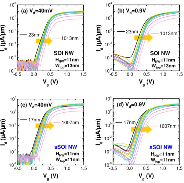
Fig. 3-5. Id-Vg characteristics as a function of Lg in the narrowest NWs for (a,b) SOI and (c,d) sSOI NMOS devices with comparison between (a,c) linear (Vd=40mV) and (b,d) saturation (Vd=0.9V) regions.
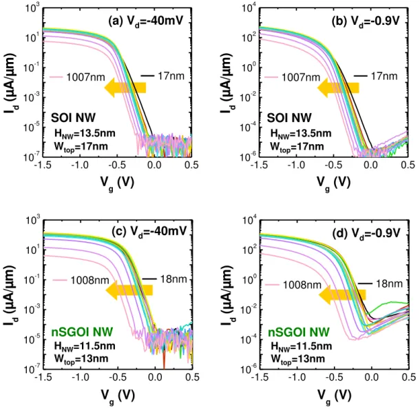
Fig. 3-6. Id-Vg characteristics as a function of Lg in the narrowest NWs for (a,b) SOI and (c,d) nSGOI PMOS devices with comparison between (a,c) linear (Vd=-40mV) and (b,d) saturation (Vd=-0.9V) regions.
Fig. 3-7. Threshold voltage Vt as a function of Lg extracted at linear (|Vd|=40mV) and saturation (|Vd|=0.9V) regions in the widest and the narrowest NW FETs for SOI (a) NMOS and (b) PMOS devices.
Fig. 3-8. Threshold voltage Vt as a function of Lg in the narrowest NMOS NWs at (a) linear (Vd=40mV) and (b) saturation (Vd=0.9V) regions for all the technological parameters.
Fig. 3-9. Threshold voltage Vt as a function of Lg in the narrowest PMOS NWs at (a,c) linear (Vd=-40mV) and (b,d) saturation (Vd=-0.9V) regions for all the technological splits.
Fig. 3-10. Extracted DIBL as a function of Lg in the widest and the narrowest NW FETs for SOI (a) NMOS and (b) PMOS devices.
List of Figures
Fig. 3-12. Extracted DIBL as a function of Lg in the narrowest PMOS NWs for all thetechnological splits.
Fig. 3-13. Subthreshold swing SS as a function of Lg in the widest and the narrowest NW FETs for SOI (a) NMOS and (b) PMOS devices.
Fig. 3-14. Subthreshold swing SS as a function of Lg in the narrowest NMOS NWs at (a) linear (Vd=40mV) and (b) saturation (Vd=0.9V) regions for all the technological parameters.
Fig. 3-15. Subthreshold swing SS as a function of Lg in the narrowest PMOS NWs at (a,c) linear (Vd=-40mV) and (b,d) saturation (Vd=-0.9V) regions for all the technological splits.
Fig. 3-16. (a) Extracted ION and (b) the gain compared with reference SOI as a function of Lg in the narrowest NMOS NWs for all the technological parameters. Fig. 3-17. (a) Extracted ION and (b) the gain compared with reference SOI as a function
of Lg in the narrowest PMOS NWs for all the technological splits.
Fig. 3-18. ION-IOFF performance in the narrowest NW (a) NMOS and (b) PMOS FETs with comparison of stressor impacts.
Fig. 3-19. Effective mobility µeff extracted as a function of Ninv in SOI TGNW and wide FETs at varying temperatures (from 300 K down to 20 K) for (a) NMOS and (b) PMOS devices.
Fig. 3-20. Effective mobility µeff extracted as a function of Ninv in SOI TGNW NMOS FETs with Wtop=10nm and Wtop=30nm at varying temperatures (from 300 K down to 20 K).
Fig. 3-21. Extraction of the (100) top and (110) side-wall mobility contributions at 300K in SOI TGNW FETs as a function of Ninv for (a) NMOS with Wtop=10nm and (b) PMOS with Wtop=30nm.
Fig. 3-22. Extraction of the µtop and µside-wall contributions at 50K in SOI TGNW FETs with Wtop=10nm as a function of Ninv for (a) NMOS and (b) PMOS devices. Fig. 3-23. Effective mobility µeff as a function of Ninv extracted at varying temperatures
for SOI TG and G NW (a) NMOS and (b) PMOS devices.
Fig. 3-24. Effective mobility µeff as a function of Ninv extracted at varying temperatures in SOI wide FET with or without additional H2 anneal process for (a) NMOS and (b) PMOS devices.
List of Figures
Fig. 3-25. Effective mobility µeff as a function of Ninv extracted at varying temperatures,showing (a) comparison between sSOI wide FET and TGNW devices, and (b) comparison between SOI and sSOI TGNW FETs.
Fig. 3-26. Effective mobility µeff at high Ninv as a function of Wtop for SOI and sSOI (a,b) NMOS and (c,d) PMOS FETs at room temperature (300K) with comparison between (a,c) TG and (b,d) G devices.
Fig. 3-27. Effective mobility µeff extracted at high Ninv as a function of temperature in (a,c) SOI and (b,d) sSOI devices for (a,b) NMOS and (c,d) PMOS FETs. Fig. 3-28. Maximum mobility µmax extracted as a function of temperature in SOI and
sSOI (a) NMOS and (b) PMOS TGNW FETs.
Fig. 3-29. Low-field mobility µ0 as a function of Lg with comparison between the widest FETs and narrowest NWs in reference SOI (a) NMOS and (b) PMOS devices.
Fig. 3-30. Low-field mobility µ0 as a function of Lg with comparison among NMOS technological splits in (a) the widest FET and (b) the narrowest NW devices. (c,d) Summary of µ0 gain compared with reference SOI case.
Fig. 3-31. Low-field mobility µ0 as a function of Lg with comparison among PMOS technological splits in (a,b) the widest FET and (c,d) the narrowest NW devices. (e,f) Summary of µ0 gain compared with reference SOI case.
Fig. 3-32. Mobility degradation factor µ in the widest FETs and narrowest NWs for all the technological parameters.
Fig. 3-33. Source/drain resistivity SD in the widest FETs and narrowest NWs for all the technological splits.
Chapter 4
Fig. 4-1. An illustration of typical noise waveform [4-1].
Fig. 4-2. A Lorentzian shaped PSD, plotted for the RTS noise waveform in Fig.4-3 [4-1].
Fig. 4-3. Schematic description of RTS noise, exemplified for a MOSFET [4-1].
Fig. 4-4. Superposition of 4 Lorentzians giving a total spectrum that approximately exhibits a 1/f dependence over several decades of frequency [4-1].
Fig. 4-5. The PSD for low-frequency noise and white noise plotted vs. frequency
List of Figures
Fig. 4-6. Schematic illustration of electrons in the channel of a MOSFET moving inand out of traps, giving rise to fluctuations in the inversion charge density and thereby the drain current [4-1].
Fig. 4-7. Simulation of the mobility fluctuation noise and carrier number fluctuation noise from subthreshold to the strong inversion regime [4-1].
Fig. 4-8. Energy band diagram showing the tunneling transitions of electrons between the conduction band and traps in the gate oxide, (i) corresponds to direct tunneling and (ii) to indirect tunneling via interface traps [4-1].
Fig. 4-9. A schematic of the LFN measurement system 3PNMS with PBA2 and DUT. Fig. 4-10. SId/Id2 as a function of frequency in the (a) SOI and (b) sSOI narrowest
-gate NW NMOS FETs with Lg~110nm, showing good 1/f behavior at threshold voltage (Vg=Vt) up to strong inversion region.
Fig. 4-11. SId/Id2 as a function of frequency in the SOI and nSGOI narrowest -gate NW PMOS FETs with Lg=107-108nm, showing good 1/f behavior at threshold voltage (Vg=Vt).
Fig. 4-12. (a) SId/Id2 as a function of frequency in the narrowest SOI -gate NW NMOS FETs with Lg=113nm, showing large 1/f2 noise components at threshold voltage (Vg=Vt). Id fluctuation as a function of time for sampling frequency of (b) f=1kHz, (c) f=40kHz, and (d) f=1MHz.
Fig. 4-13. (a) SId/Id2 as a function of frequency in the narrowest SOI -gate NW NMOS FETs with Lg=28nm, showing large 1/f2 noise components at threshold voltage (Vg=Vt). Id fluctuation as a function of time for sampling frequency of (b) f=1kHz, (c) f=40kHz, and (d) f=1MHz.
Fig. 4-14. SId/Id2 as a function of frequency in the narrowest SOI -gate NW NMOS FETs with (a) Lg=113nm and (b) short channel Lg=23-28nm, showing 1/f behavior in low-frequency region at threshold voltage (Vg=Vt).
Fig. 4-15. Id dependent (symbols) SId/Id2 and (lines) corresponding (gm/Id)2 curve characteristics normalized by channel size parameters (Wtot and Lg) in reference SOI wide FETs and the narrowest NWs compared with (a) [100]-oriented SOI, (b) SOI with additional H2 anneal, and (c) sSOI for NMOS devices.
Fig. 4-16. Id dependent (symbols) SId/Id2 and (lines) corresponding (gm/Id)2 curve characteristics normalized by channel size parameters (Wtot and Lg) in wide FETs and the narrowest NWs for (a) SOI, (b) nSG-S/D, and (c) nSGOI for PMOS devices.
List of Figures
Fig. 4-17. Comparison of 3-types of PMOS device variants; SOI, nSG-S/D, and nSGOI,in Id dependent (symbols) SId/Id2 and (lines) corresponding (gm/Id)2 curve characteristics normalized by Wtot and Lg for (a) wide FETs and (b) the narrowest NWs.
Fig. 4-18. Schematic of defects in spacers 1 and 2 and/or in Si film contributing to RSD fluctuations in SOI MOSFET architecture.
Fig. 4-19. Id dependent (symbols) SId/Id2 and (lines) corresponding (gm/Id)2 curves with consideration of the scµeff and SRsd term shown in Eq. (4-28), showing (a) the narrowest NW vs. wide FETs in SOI devices, and SiGe S/D vs. SGOI devices in (b) NWs, and in (c) wide FETs.
Fig. 4-20. Hooge parameter H as a function of gate voltage overdrive Vgt for various technological splits in the narrowest (a) NMOS and (b) PMOS NW FETs. Fig. 4-21. (Symbols) SVg1/2 versus Id/gm characteristics and (lines) the linear regression
for extraction of SVfb and scµeff in (a) wide and (b) 1ch-TGNW both N- and PMOS FETs.
Fig. 4-22. SVfb as a function of (a) Wtot and (b) Lg for all the technological splits in NMOS devices.
Fig. 4-23. SVfb as a function of (a) Wtot and (b) Lg for all the technological parameters in PMOS devices.
Fig. 4-24. Coulomb scattering parameter αscμeff as a function of the channel area WtotLg in all the devices with single-channel for (a) NMOS and (b) PMOS FETs. Fig. 4-25. Coulomb scattering parameter αscμeff as a function of low-field mobility µ0
extracted in Figs.3-30b and 3-31d for the narrowest NW (a) NMOS and (b) PMOS FETs.
Fig. 4-26. Nt as a function of (a) Wtot and (b) Lg for all the technological splits in NMOS devices.
Fig. 4-27. Nt as a function of (a) Wtop and (b) Lg for all the technological parameters in PMOS devices.
Fig. 4-28. Nt averaged for Lg in wide and NW FETs for (a) NMOS and (b) PMOS devices, with comparison between SOI and sSOI for NMOS, and among SOI, cSG-S/D, and nSGOI for PMOS.
Fig. 4-29. (a) Demonstration of the extraction and (b) the extracted Nt contribution of top surface and side-walls by the Nt separation method for all the NMOS devices
List of Figures
Fig. 4-30. (a) Demonstration of the extraction and (b) the extracted Nt contribution oftop surface and side-walls by the Nt separation method for all the PMOS devices.
Fig. 4-31. Schematics of the experimental set-up used for charge pumping spectroscopy
[4-94].
Fig. 4-32. Mean Dit obtained by CP measurement as a function of Wtop in wide gated P-i-N diode and 75-multiple channel NW devices.
Fig. 4-33. Vd impact for SId/Id2-Id characteristics of the narrowest NW NMOS FETs in (a) SOI (Lg=113nm) and (b) sSOI (Lg=107nm).
Fig. 4-34. Vd impact for SId/Id2-Id characteristics of the narrowest NW PMOS FETs with short channel in (a) SOI (Lg=17nm) and (b) nSGOI (Lg=23nm).
Fig. 4-35. (Symbols) SVg with normalization by channel size parameters (Wtot and Lg) and frequency as a function of Vd in the (a) SOI and (b) sSOI narrowest NW NMOS FETs.
Fig. 4-36. Comparison of the normalized SVg between our experimental data and ITRS requirements in 2015 and 2026 in NMOS MG FETs [4-95].
Fig. 4-37. (Symbols) SVg with normalization by channel size parameters (Wtot and Lg) and frequency as a function of Vd in the narrowest NW PMOS FETs for (a) SOI, (b) cSG-S/D, and (c) nSGOI devices.
Fig. 4-38. Comparison of the normalized SVg between our experimental data and ITRS requirements in 2015 and 2026 for PMOS MG FETs [4-95].
List of Symbols, Acronyms, and Abbreviations
Symbol Unit Meaning Cacc F (F/cm2) Accumulation layer capacitance (per channel area) CBOX F (F/cm2) Buried-oxide capacitanceCdep F (F/cm2) Depletion layer capacitance Cgb F (F/cm2) Gate-to-body capacitance Cgc F (F/cm2) Gate-to-channel capacitance
Cin F Input capacitance
Cinv F (F/cm2) Inversion layer capacitance Cit F (F/cm2) Capacitance of interfacial traps
Cit_BOX F (F/cm2) Capacitance of traps at Si/BOX interface
Cload F Total load capacitance
Cout F Output capacitance
Cox F (F/cm2) Gate oxide capacitance Ctot F (F/cm2) Total capacitance
Cwire F Wiring capacitance
Dit eV-1cm-2 Density of interface traps
EC eV Conduction band edge energy
Eeff V/cm Effective electric field
EF eV Fermi level
Ei eV Intrinsic Fermi level
EV eV Valence band edge energy
f Hz Frequency (operating frequency = clock frequency)
fmax Hz Maximum operating frequency
fp Hz Frequency of pulse signal in CP technique
gm S Transconductance
h Js Planck's constant (=6.626×10⁻³⁴)
HNW cm Channel height of nanowire
I A Current
ICP A Maximum charge pumping current
Id A (µA/µm) Drain current (normalized by channel width) Id_lin A Drain current in linear region
Id_sat A Drain current in saturation region Id_sub A Drain current in subthreshold region
Ileak A Off-state leakage current
ION A (µA/µm) On-state drain current
Iox A Leakage current due to gate oxide tunneling Isat A (µA/µm) Saturated on-current in short channel devices
Isc A Direct short-circuit current
Isub A Subthreshold leakage current
I(t) A Time dependent fluctuating current
i(t) A Randomly fluctuating component of current k J/K Boltzmann's constant (=1.38×10⁻²³)
K Proportional constant
L cm Channel length
Lg cm Gate length
List of Symbols, Acronyms, and Abbreviations
Symbol Unit Meaningn cm-2 Electron density
n Effective number of gate
N Number of conducting carriers
NA cm-2 Acceptor (hole) doping density
Nch Number of parallel channel finger
ni Intrinsic carrier density in the substrate Ninv cm-2 Inversion carrier density
Nt eV-1cm-3 Oxide trap density
Nt_side-walls eV-1cm-3 Oxide trap density in the channel side-walls Nt_top eV-1cm-3 Oxide trap density in the channel top
p cm-2 Hole density in the substrate
Pall W Overall power consumption
Psc W Direct short-circuit power consumption
Pst W Static power consumption
Psw W Dynamic switching power consumption
q C Elementary charge (=1.602×10⁻¹⁹) Qdep C/cm2 Depletion charge density
Qinv C/cm2 Inversion charge density Qox C/cm2 Oxide charge density
R Resistance
R(s) Autocorrelation function
RSD Source/drain series resistance
S(f) Power spectral density
SI A2/Hz Power spectral density of current noise
SId A2/Hz Power spectral density of the drain current noise SR 2/Hz Power spectral density of the resistance fluctuations SRsd 2/Hz Power spectral density of the RSD fluctuations SV V2/Hz Power spectral density of voltage noise
SVfb V2/Hz Power spectral density of the flat-band voltage noise SVg V2/Hz Power spectral density of the gate voltage noise t s Time
T K Absolute temperature
Thigh-k cm High- gate dielectric thickness
Tox cm Gate oxide (insulator) thickness tsc s Duration of direct short-circuit
TSi cm Si film thickness
TSiO2 cm Gate silicon dioxide thickness
tsw s Duration of switching
V V Voltage
Vbase V Base level of gate voltage pulse in CP technique Vch V Potential along the channel
Vd V Drain (-to-source) voltage
Vdd V Power supply voltage
Vd_lin V Drain voltage in linear region Vd_sat V Drain voltage in saturation region
List of Symbols, Acronyms, and Abbreviations
Symbol Unit MeaningVg V Gate voltage
Vgt V Gate voltage overdrive (=|Vg-Vt|)
Vin V Input voltage
vinj cm/s Injection velocity of carriers vlim cm/s Limiting velocity of carriers
Vout V Output voltage
vsat cm/s Saturation velocity of carries
Vt V Threshold voltage
Vt_lin V Threshold voltage in linear region Vt_sat V Threshold voltage in saturation region
W cm Channel width
Wdep cm Depletion layer width
WSi cm Si body width
Wtop cm Top-view channel width
Wtot cm Total effective channel width
x(t) Variable in time domain
X(f) Fourier-transformed variable in frequency domain z cm Oxide trap location from the channel interface
E J, eV Energy splitting
Eg_Si eV Band gap energy of Si (=1.12)
f Hz Loss of operating frequency by DIBL effect I A Difference between two current levels in RTS Id A Fluctuating (AC) component of drain current N2
Variance of the fluctuating number of carriers
Vg V Constant amplitude of trapezoidal gate voltage pulse
in CP technique
Generalized scaling factor of electric field
H Hooge parameter
sc Vs/C Coulomb scattering coefficient
sw Switching activity rate
µ nmVs/cm2 Mobility degradation factor
Proportionality constant
0 µA/V2 Transistor (transconductance) gain
Frequency or temperature exponent
Qox Fluctuation of oxide charge Vfb Fluctuation of flat-band voltage
µeff Fluctuation of carrier effective mobility 0 F/cm Permittivity in vacuum (=8.854×10⁻¹⁰)
ox Relative permittivity of gate oxide
Si Relative permittivity of silicon (=12)
SiO2 Relative permittivity of silicon dioxide (=3.9)
List of Symbols, Acronyms, and Abbreviations
Symbol Unit Meaning Empirical parameter for Eeff definition Scaling factor of MOSFET or chip size
cm Attenuation length of carrier wave function in oxide n cm Natural length (parameter with respect to SCE) µ0 cm2/Vs Low-filed mobility
µC cm2/Vs Mobility limited by Coulomb scattering µconst cm2/Vs Assumed constant mobility along the channel µeff cm2/Vs Effective mobility
µmax cm2/Vs Peak mobility µn cm2/Vs Electron mobility
µP cm2/Vs Mobility limited by phonon scattering µsat cm2/Vs Effective mobility in saturation region µside-wall cm2/Vs Effective mobility in the channel side-walls µSR cm2/Vs Mobility limited by surface roughness scattering µTG cm2/Vs Effective mobility in tri-gate nanowire devices µtop cm2/Vs Effective mobility in the channel top
µY cm2/Vs Mobility approximated by Y-function method L Pa-1 Longitudinal piezoresistive coefficient
1, 1.0 V-1 First order mobility attenuation factor 2 V-1 Second order mobility attenuation factor C/cm2 Local charge density
SD m Source-drain series resistivity
S/cm Conductivity
stress Pa Applied stress in the longitudinal direction s Time constant of carrier transitions
s Time constant based on SRH process (often =10-10) h s Duration for higher current state in RTS
l s Duration for lower current state in RTS
phonon s Relaxation time due to intervalley phonon scattering trap s Relaxation time due to intervalley phonon scattering ms eV Work function difference between gate and channel
materials
B eV Tunneling energy barrier height
B V Difference between EF and Ei potentials (=|EF-Ei|/q) Bp V B in p-type substrate (NMOS)
S V Surface potential (band bending of substrate)
3PNMS Programmable Point Probe Noise Measuring System
AC Alternate current
ALD Atomic layer deposition
BEOL Back-end of line
BOX cm Buried oxide
CESL Contact etch stop layer
List of Symbols, Acronyms, and Abbreviations
Symbol Unit MeaningCNF Carrier number fluctuations
C-V Capacitance-voltage
CVD Chemical vapor deposition
DC Direct current
DG Double gate
DIBL mV/V Drain induced barrier lowering
DUT Device-under-test
DUV Deep ultraviolet
e-beam Electron beam
CMP Chemical mechanical polishing
CP Charge pumping
EOT cm Equivalent oxide thickness
FD Fully depleted
FET Field-effect transistor
GAA Gate-all-around
g-r Generation-recombination
high- High dielectric constant (permittivity)
HDD Highly doped drain
HH Heavy holes
HP High performance
IC Integrated circuit
IL Interfacial layer
ITRS International Technology Roadmap for Semiconductors
LCR Inductance (L) - capacitance (C) - resistance (R)
LDD Lightly doped drain
LFN Low frequency noise
LH Light holes
LNA Low noise amplifier
LSTP Low standby power
MF Mobility fluctuations
MG Multi-gate
MOSFET Metal-oxide-semiconductor field-effect transistor
NMOS N-channel MOS
NW Nanowire
PBA Programmable biasing amplifier
PD Partially depleted
PDP J Power-delay product
PMOS P-channel MOS
poly- Polycrystalline
PR Piezoresistance
PSD Power spectral density
QM Quantum-mechanical
RF Radio frequency
RTS Random-telegraph-signal
List of Symbols, Acronyms, and Abbreviations
Symbol Unit MeaningSEM Scanning electron microscopy
SGOI SiGe-on-insulator
SOI Silicon-on-insulator
SRB Strained-relaxed buffer
SS mV/dec Subthreshold swing
sSi Strained-Si
sSOI Strained-Si-on-insulator
TEM Transmission electron microscopy
Tri-gate (TG) Triple-gate
-gate (G) Omega-gate
Chapter 1. Introduction
Chapter 1
Introduction
1.1 General Context
1.2.1 MOSFET downscaling -Moore's law-
1.2.2 Power consumption of CMOS logic circuits
1.2.3 End of scaling era?
1.2 Purposes and scopes of this work
Chapter 1. Introduction
1.1 General Context
1.2.1 MOSFET downscaling -Moore's law-
Metal-oxide-semiconductor field-effect transistor (MOSFET) is the core technology of today's microelectronics. MOSFETs are mainly used as switches in logic microcircuits, and the devices can also fulfill other purposes. A modern microprocessor can contain more than 7 billion MOSFETs. Moreover, 128-gigabyte memory card contains 1024 billion (over 1 trillion) MOSFETs, while the card only weighs approximately 0.4g. 1 trillion is comparable to the number of fixed stars in the Andromeda Galaxy, which is the largest galaxy in the local group of galaxies included the Milky Way Galaxy, the solar system, and the earth where we live.
The concept of MOSFET was first invented around 1925-30 by Julius Lilienfeld [1-1,1-2]. After the development of point-contact transistor in 1947 by William Shockley, John Bardeen, and Walter Brattain [1-3], Martin Atalla and Dawon Kahng developed first MOSFET in 1959 [1-4]. The MOSFET technology was combined with the invention of integrated circuit (IC) in 1958 by Jack Kilby (and also by Robert Noyce) [1-5,1-6], and the growth has been accelerated and continued over 50 years up to the present days. The huge growth of semiconductor industry mainly based on silicon devices has lead to the miniaturization, the price drop, and the performance enhancement for lots of appliances and multimedia applications, such as computers and mobile phones.
In 1965, Gordon Moore published a paper [1-7], in which he predicted that density of MOSFETs on a chip would increase twice every 18 months. Although this “Moore's law” is empirically based on data within only 6 years between 1959 when the first Si IC was fabricated and 1965, the law has held amazingly up to the present, over 45 years (Fig.1-1). This clearly means that size reduction of MOSFETs allows increase of the density in an IC chip. The circuit capability thus increases for a constant chip size. However, there are other motivations for downscaling of MOSFET size. Double increase of MOSFETs density in a chip provides reduction of the chip dimensions, which are the length and width, divided by 21/2. This scaling rate is usually represented
Chapter 1. Introduction
as a factor of . In 1974, Dennard et al. published a paper [1-8], and he expressed the scaling benefits. Based on the ideal supposition for maintaining a constant electric field inside the MOSFET, device scaling by the factor (i.e. twice the integration density) increases the switching speed by and reduces the power dissipation by 2. Table 1-1 shows the scaling MOSFET and circuit parameters under the constant field scaling and the generalized scaling rules [1-9]. The generalized scaling rule assumes that the electric field intensity changes by a factor of . Dennard's law was suitable for the chip scaling until around 2005. After, the conventional scaling ended, and the performance enhancement originating from the device scaling, such as microprocessor clock frequency, has been saturated. This performance saturation has been caused by short-channel effects (SCE), which appeared in MOSFETs with aggressively shortened distance between the source and drain regions. Unfortunately, it is anticipated that SCE becomes more salient as the length is downscaled.
Table 1-1. Scaling MOSFET device and circuit parameters [1-9].
2
2
Circuit density (~ 1/A)
2/3
1/3
Power-delay product per circuit (P)
2/2
3/2
1/2
Power dissipation per circuit (P ~ VI)
/ 1 1/ 1 Channel resistance (Rch) 2/ 1/ Drift current (I)
1
Inversion-layer charge density (Qinv)
1/ 1/ Capacitance (C=A/t) / 1/ Voltage (V) Doping concentration (NA, ND) 1 1/ 1/
Depletion-layer width (Wdep)
1
Carrier velocity (v)
Generalized scaling
Constant-field scaling Long Ch. Short Ch.
1/ 1/
1/ Circuit delay time (~ CV/I)
Derived scaling behavior of circuit parameters
1
Electric field (E) Derived scaling behavior of device parameters 1/ 1/ Device dimensions (tox, W, L) Scaling assumptions Multiplicative factor (>1) MOSFET device and circuit parameters
2
2
Circuit density (~ 1/A)
2/3
1/3
Power-delay product per circuit (P)
2/2
3/2
1/2
Power dissipation per circuit (P ~ VI)
/ 1 1/ 1 Channel resistance (Rch) 2/ 1/ Drift current (I)
1
Inversion-layer charge density (Qinv)
1/ 1/ Capacitance (C=A/t) / 1/ Voltage (V) Doping concentration (NA, ND) 1 1/ 1/
Depletion-layer width (Wdep)
1
Carrier velocity (v)
Generalized scaling
Constant-field scaling Long Ch. Short Ch.
1/ 1/
1/ Circuit delay time (~ CV/I)
Derived scaling behavior of circuit parameters
1
Electric field (E) Derived scaling behavior of device parameters 1/ 1/ Device dimensions (tox, W, L) Scaling assumptions Multiplicative factor (>1) MOSFET device and circuit parameters
Chapter 1. Introduction
As shown in Fig.1-1 [1-10], minimum feature size of MOSFETs, which corresponds to the gate length, has been downscaled from 10μm down to 28nm (yellow circles; right y axis) between 1970 and 2011. In parallel, the number of MOSFETs per square millimeter (mm-2) increased from 200 to over 1 million (other objects show data for the four main microprocessor manufacturers; left y axis). The gate length in the current MOSFET generation lies between 22nm and 17nm. In practice, the distance between the source and the drain is approximately 50% shorter than the gate length, resulting in an effective channel length of only ~10nm. It is predicted that the effective channel length will approach about 5nm in 2020, which is only ten-fold size of the lattice parameter of a silicon crystal.
Fig. 1-1. The evolution of MOSFET minimum feature size (gate length) and the density of MOSFETs in microprocessors over time[1-10].
1.2.2 Power consumption of CMOS logic circuits
The most basic component of digital logic microcircuits is a complementary-MOS (CMOS) inverter as a switch. The CMOS configuration was first invented in 1963 by Frank Wanlass [1-11,1-12]. It consists of a symmetrical pairs of two types of MOSFETs, which are an n-channel MOSFET (NMOS FET) and a p-channel MOSFET (PMOS FET), as shown in Fig.1-2a. The source terminal of the NMOS FET is grounded, while the supply voltage Vdd is applied to the PMOS FET source. The gates of both MOSFETs are connected and common signal is input to the gates. The drains are also connected as
Chapter 1. Introduction
the output node. The Cload is the total load capacitance including the output capacitance Cout, the input capacitance Cin, and the wiring capacitance Cwire.
The current through the PMOS FET (IP) flows from the source into the drain and charges up the output voltage to Vdd (pull-up), meanwhile the current through the NMOS FET (IN) flows from the drain into the grounded source and discharges the output voltage to zero (pull-down), as shown in Fig.1-2b and c. In CMOS system, the complementary essence allows only one of the MOSFETs to be switched-on (i.e. one FET of the pair is always switched-off). In principle, the power dissipation thus occurs only during momentary switching when the charging or discharging current flows through the inverter. Therefore, CMOS system dissipates significantly less static power and has higher noise immunity than other logic circuits with resistive loads, such as transistor-transistor logic (TTL) and NMOS logic. Moreover, CMOS process allows a high-density integration of logic functions on an IC. Since these advantages have been efficiently improved, the huge majority of modern IC manufacturing is based on CMOS processes. Source Drain Drain Gate Gate Source Cload Out PMOS NMOS In Vdd Cload Vout PMOS Vin Vdd IP Cload NMOS Vdd Vout Vin IN (a) (b) (c)
Fig. 1-2. (a) Circuit schematic of CMOS inverter. Equivalent circuits of (b) pull-up and (c) pull-down conditions.
Overall power consumption Pall in a CMOS logic IC is defined by the sum of dynamic switching power Psw, direct short-circuit power Psc, and static power Pst as [1-13,1-14]:
Chapter 1. Introduction
st sc sw all P P P P (1-1) with Psw
swCloadVdd2f (1-2) f V I t Psc
sw sc sc dd (1-3)
sw
leak dd
sw
sub ox
dd st I V I I V P 1
1
(1-4)where sw is the switching activity rate, f is the operating frequency (clock frequency),
tsc is the required short-circuit time, Isc is the short-circuit current flowing directly from
the Vdd line to the ground line, and Ileak is the off-state leakage current. The Ileak is
divided into two components: the subthreshold leakage current Isub and the tunneling
current in the gate oxide Iox. Generally, the power consumption Pall is dominated by the
dynamic component Psw and is reduced by the scaling factor 2. Furthermore, the
average energy consumed per switching operation can be reduced by 3. The average switching energy, also known as the power-delay product (PDP), is a figure of merit about energy efficiency in logic circuits. It is the product of dynamic power consumption and duration of the switching tsw (=1/f), thus the PDP is expressed as:
2 dd load sw sw sw sw C V f P t P PDP
(1-5)As mentioned above, the Pst leakage is negligible in theory since CMOS circuits
dissipate power only during switching, and it is the primary advantage of CMOS system.
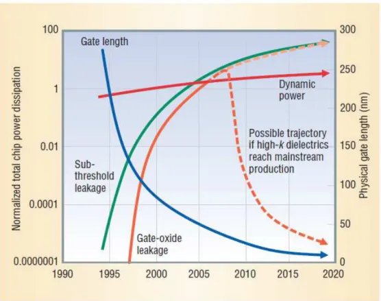
In practice, however, the continuing MOSFET scaling and the resulting circuit density growth has recently caused an unacceptable level of the Pst. Figure 1-3 shows the power consumption trends in CMOS logic IC chips [1-14]. As the size of MOSFETs is decreased with each advanced process technology, the clock frequency of CMOS circuits is increased. As a result, the dynamic switching power Psw has been increased year by year. On the other hand, the static power consumption Pst, which is the sum of the subthreshold leakage and the gate oxide leakage components, is exponentially increased by shortening the gate length of MOSFET. Particularly, the Pst exceeds the Psw after 2005 in the prediction. Therefore, reduction of the Pst has been a major challenge for recent CMOS technology node.
Increase of the Isub is mainly due to short-channel effects (SCE). Meanwhile Iox is increased owing to the aggressively scaled gate oxide thickness for enhancement of the
Chapter 1. Introduction
electrostatic gate control. This gate oxide leakage can be reduced by replacing the conventional gate insulator, silicon dioxide (SiO2), with materials with higher dielectric constant (high-). For the issue of Isub increase, change of the gate architecture has been proposed in order to effectively enhance the electrostatic gate control.
Fig. 1-3. Total chip dynamic and static power dissipation trends based on the International Technology Roadmap for Semiconductors.[1-14].
1.2.3 End of scaling era?
Unfortunately, MOSFETs are thus not perfect switches. The off-current is not zero, the on-current is limited by semiconductor resistance, and the switching takes longer time. Moreover, the switching does not occur suddenly at exact gate voltage bias but needs some voltage range and the gradual change. Furthermore, the switching behavior and the leakage power consumption are degraded by SCE as the size of MOSFET is downscaled, and it has been a serious issue for recent and future technology nodes.
Chapter 1. Introduction
instance, recent MOSFET structures released by Intel are shown in Fig.1-4 [1-15]. Some solutions to overcome the deterioration of the switching properties have been considered by using novel technologies, such as silicon-on-insulator (SOI) substrate [1-16,1-17] (Fig.1-5 [1-18]) and 3D multi-gate (MG) structures [1-10] (such as Tri-Gate device in Fig.1-4). For further performance improvement, solutions to the resolution limit of optical lithography, alternative oxide/metal gate, and high-performance channel materials have been also investigated as well.
Fig. 1-4. Recent MOSFET architectures and process nodes released by Intel Corporation [1-15].
Chapter 1. Introduction
Fig. 1-5. Schematic of MOSFET structure based on silicon-on-insulator (SOI) technology [1-18].
Figure 1-6 shows the schematic of future device technology as reported by the international technology roadmap for semiconductors (ITRS) in 2011 [1-19]. The gate-stack, composed of high- dielectric/metal gate materials instead of SiO2/Poly-Si, has been practically introduced from the 45nm process node in 2007 by Intel (Fig.1-4). This technology is going to be maintained and the materials will be further optimized to obtain better gate control and lower gate leakage current Iox. For high-speed operating devices, strained Si channel exhibiting higher carrier mobility has been intensively investigated. Moreover, substitute materials, such as Ge and III-V compounds, have been also studied to achieve much higher mobility. As mentioned above, SOI and MG technologies have been proposed to improve electrostatic control by the gate and strongly reduce the SCE (i.e. Isub). First commercial MG MOSFET was released in 2011 by Intel, using the structure of a bulk FinFET [1-20] (Fig.1-4). For the next device generation, MG with extremely shrunk body (nanowire) on bulk or SOI substrates has been intensely expected. The gate length of MOSFET should become sub-10nm within 10 years, and approach 6-7nm in 2026. It is awaited that performance requirements
Chapter 1. Introduction
Fig. 1-6. ITRS 2011 “equivalent scaling” process technologies timing compared to overall roadmap technology characteristics (ORTC) and industry “node” naming [1-19]. 2015 2020 2025 0 5 10 15 20 25 L g ( n m ) Year HP LSTP
(a) Gate length L
gITRS2013
Requirement for MG
2015 2020 2025 0.4 0.6 0.8 1.0 0.2 0.3 0.4 0.5 V dd ( V ) Year V d = V dd /2 (V) HP LSTPITRS2013
Requirement for MG
(b) V
dd& V
dFig. 1-7. ITRS requirements for future high performance (HP) and low standby power (LSTP) logic circuits consisting of MG FETs. (a) MOSFET gate length Lg, and (b)
circuit supply voltage Vdd and MOSFET drain voltage Vd are plotted as a function of
year between 2015 and 2026 (sourced from ITRS 2013 data in Table RFAMS1 CMOS technology requirements [1-21]).
Chapter 1. Introduction
1.2 Purposes and scopes of this work
Future MOSFET technology node should require MG architectures. However, it became difficult to rigorously examine the electrical characterizations of MG FETs, especially for NW devices, with general characterization method based on capacitance measurement (such as split C-V). Low-frequency noise (LFN) also provides deep insights into electrical properties of the gate oxide/channel interface in MOSFETs [1-22]. LFN characterization has no lower limit of the necessary MOSFET channel area. Therefore, LFN measurement can be a powerful characterization technique for ultra-scaled NW MOSFETs. From engineering point of view, LFN can be a problem in RF/analog circuits. LFN cannot be completely eliminated and sets a lower limit on signal detection in analog devices and circuits. For instance, when excess LFN (1/f noise) stemming from MOSFET appears in phase noise of voltage-controlled-oscillators (VCO), the signal-to-noise ratio (SNR) in mixers for homodyne receivers is degraded. Consequently, measurements and understanding of LFN are highly important in order to evaluate the electrical interface properties and the performance in MOSFETs.
Nowadays, a large number of reports for LFN measurement even in MG devices (for FinFETs [1-23~1-35] and for NW FETs [1-36~1-45]) have been published. Concerning LFN characterizations in recent MG devices, the origin of 1/f noise is mainly attributed to unified carrier number fluctuations with correlated fluctuations (CNF+CMF). Hung et al. suggested the CNF+CMF model in 1990 [1-46], and then Ghibaudo et al. proposed a more popular definition [1-47]. In practice, the model is mainly suitable for MG devices and have been discussed in previous reports [1-23~1-25,1-28,1-32~1-34,1-36,1-38~1-45]. However, few reports of comprehensive study on each parameter defined in the CNF+CMF model as functions of MOSFET channel size (Wtop and Lg), architectural difference (planar vs. MG), and technological parameters (channel orientation, strain, etc…), have been published.
In intensive investigations of high-/metal gate stack, a number of researches for Hf-based gate dielectric have been reported in MG FinFETs [1-25,1-28~1-34]. But, /metal gate stack. Tachi et
Chapter 1. Introduction
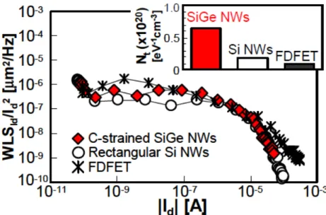
al. reported a figure exhibiting LFN behavior of vertically-stacked GAA NWs in 2009,as shown in Fig.1-8 [1-39]. They found that the trap density of Si NWs is higher than the value of planar FD FET. Therefore, there is a concern about the degraded interface quality in NW FETs with Hf-based high-/metal gate.
Fig. 1-8. Low-frequency noise of Si and c-strained SiGe NWs. Inserted figure is a comparison of oxide trap density (Nt). LG and WNW are ~290nm and ~20nm,
respectively [1-39].
Similarly with the report by Tachi et al., Zhuge et al. reported LFN characterization of GAA NW with thermal Si oxide (SiO2) with higher oxide trap density than conventional SiO2/poly-Si gate stack in 2009 [1-36]. They considered that the degradation could be caused by various surface orientations and small diameter of GAA NW. On the other hand, Crupi et al. reported similar values of oxide trap density between tri-gate and planar NMOS FETs with SiON/poly-Si gate stack in 2006, as shown in Fig.1-9 [1-23]. Contributions of different crystallographic orientations of channel surface among the interfaces (i.e. MG top (and bottom) surface vs. side-walls) into oxide trap density should be thus evaluated in detail.
Chapter 1. Introduction
Fig. 1-9. Effective trap density versus gate voltage overdrive for the 30-fin triple-gate devices (WFIN=60nm, L=1μm) and planar devices (W×L=1μm×1μm). No significant
difference between the two structures is observed. [1-23].
Meanwhile, LFN level decrease was observed in SOI tri-gate NW FETs with SiO2/poly-Si by Feng et al. in 2011 [1-42], and in GAA Si NWFETs with SiO2/TiN by Lee et al. in 2012 as shown in Fig.1-10 [1-43]. It could be ascribed to quantum confinement of carriers due to large surface/volume ratio of NW. This volume inversion impact may also be observed in aggressively scaled NWs with Hf-based high-k/metal gate stack.
Chapter 1. Introduction
Fig. 1-10. Averaged noise spectral densities (symbols) <SId/Id 2
> and (lines) <(gm/Id) 2
> versus Id at Vd=0.1V and f=10Hz for 7-, 9-, and 12-nm dNW, respectively. All the left
axes represent <SId/Id 2
>, whereas all the right axes (red colored) represent <(gm/Id) 2
> multiplied by a constant. The symbols within the dotted circle at the same current level (1μA) are for the comparison of <SId/Id
2
> for each dNW. [1-43].
Influence of strain technology into the interface quality has also been a significant concern and has been studied. For improvement of NMOS performance, tensile strained Si fabricated on SiGe virtual layers has been used and reported the LFN characteristics mostly for planar FETs [1-22,1-48~1-54]. The upgraded [1-48~1-50], constant [1-22], and degraded [1-51~1-54] LFN results compared with reference Si devices. For example, Fig.1-11shows a deteriorated oxide trap density with increase of Ge content in strained-relaxed-buffer (SRB) SiGe virtual layer reported by Wang et al. in 2007[1-54]. LFN data of sSi NW is necessary for future CMOS node.
Chapter 1. Introduction
Fig. 1-11. Relationship between equivalent oxide traps per unit area Nt and scattering
parameter α and with different Ge content of SRB layers. [1-54].
For PMOS enhancement, compressive strained channel has been fabricated by SiGe source/drain (S/D) and SiGe channel formations. There are few reports of LFN study for SiGe S/D technique in planar [1-55~1-57] and NW [1-45] FETs. LFN properties for SiGe channel FinFETs [1-29~1-31] and NWs [1-37,1-38] have been investigated. However, as Tachi et al. reported a 3.5 times higher oxide trap density for SiGe NWs than for Si NWs (Fig.1-8[1-39]), there is still a concern about the interface quality.
As a consequence, important concerns for ultra-scaled NW MOSFETs should be discussed in detail as follows;
(i) CNF+CMF model parameters as a function of channel size down to NW (ii) NW FETs with advanced Hf-based high-/metal gate stack
(iii) Contributions of different crystallographic orientations of channel surface (iv) Large channel surface/volume ratio in NW
(v) Strained NW technology;
NMOS - tensile strain PMOS - compressive strain
Chapter 1. Introduction
Accordingly, the purpose of this work is experimental and comprehensive investigation of electrical characteristics in gate oxide/channel interface by LFN and carrier transport measurements in ultra-scaled NW MOSFETs with Hf-based high-/metal gate stack, in order to evaluate the significant concerns of (i)-(v).
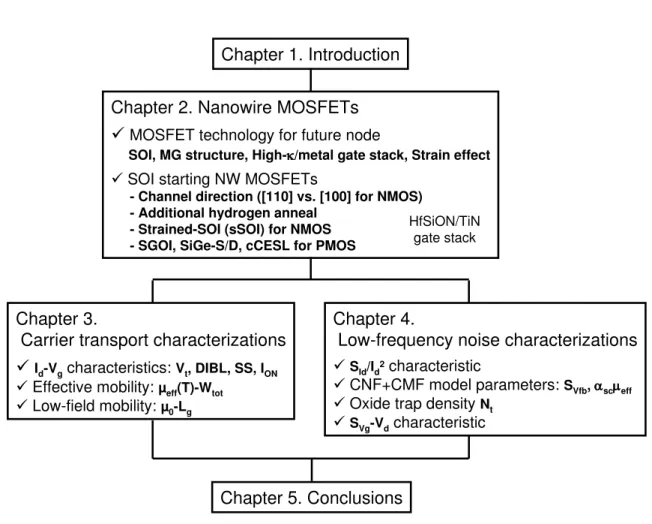
Our silicon nanowire (NW) MOSFETs were fabricated from advanced fully-depleted SOI (FD-SOI) substrate, and with Hf-based high-/metal gate stack (HfSiON/TiN) in order to suppress detrimental SCE and gate leakage. In addition, strain introduction technologies to the channel were additively processed to efficiently improve the MOSFET's performance. Tensile strained-SOI substrate was used for NMOS FETs, whereas compressive stressors were used for PMOS devices. Compressively strained Si channel can be processed by raised SiGe S/D and contact-etch-stop-layer (CESL) formations. In addition, strained SiGe-on-insulator channel was also fabricated for further high-performance PMOS FETs. These fabrication technologies and processes are described in detail in chapter 2.
The gate oxide/channel interface characteristics in the various NW MOSFETs are examined on carrier transport characterizations as the channel properties in chapter 3, and LFN characterizations for the interface properties in chapter 4. In chapter 3, DC gate voltage dependent drain current (Id-Vg), temperature dependent effective mobility (µeff), and low-field mobility (µ0) characteristics are investigated. In chapter 4, drain current noise SId/Id2 behavior, parameter evaluations based on advanced 1/f noise model (involving flat-band voltage noise SVfb, Coulomb scattering parameter scµeff, and oxide trap density Nt), and drain bias dependent gate voltage noise (SVg-Vd) behavior compared with the ITRS requirements are characterized.
Finally, our study on electrical characterizations for the oxide/channel interface in NW MOSFETs is concluded in chapter 5. The perspective of LFN investigation on future device nodes is described.

![Fig. 2-4. The drain current as a function of the gate voltage in a MOSFET [2-1].](https://thumb-eu.123doks.com/thumbv2/123doknet/12856195.368248/58.892.210.684.195.494/fig-drain-current-function-gate-voltage-mosfet.webp)
![Fig. 2-8. Illustration of C tot -V g characteristic in bulk Si NMOS FET (Illustration of QM and poly-silicon depletion effects on C-V) [2-17]](https://thumb-eu.123doks.com/thumbv2/123doknet/12856195.368248/63.892.216.669.537.868/fig-illustration-characteristic-nmos-illustration-silicon-depletion-effects.webp)
![Fig. 2-10. Dependence of DIBL and SS on the scaling parameter [2-21].](https://thumb-eu.123doks.com/thumbv2/123doknet/12856195.368248/67.892.235.678.188.852/fig-dependence-dibl-ss-scaling-parameter.webp)
![Fig. 2-13. Band gap energy as a function of relative permittivity for various dielectrics [2-43~2-45]](https://thumb-eu.123doks.com/thumbv2/123doknet/12856195.368248/71.892.239.649.581.891/fig-band-energy-function-relative-permittivity-various-dielectrics.webp)