HAL Id: tel-01699426
https://tel.archives-ouvertes.fr/tel-01699426
Submitted on 2 Feb 2018HAL is a multi-disciplinary open access archive for the deposit and dissemination of sci-entific research documents, whether they are pub-lished or not. The documents may come from teaching and research institutions in France or abroad, or from public or private research centers.
L’archive ouverte pluridisciplinaire HAL, est destinée au dépôt et à la diffusion de documents scientifiques de niveau recherche, publiés ou non, émanant des établissements d’enseignement et de recherche français ou étrangers, des laboratoires publics ou privés.
Physical modelling of junction fabrication processes on
FDSOI substrate for the 10 nm node and below
Anthony Payet
To cite this version:
Anthony Payet. Physical modelling of junction fabrication processes on FDSOI substrate for the 10 nm node and below. Micro and nanotechnologies/Microelectronics. Université Grenoble Alpes, 2017. English. �NNT : 2017GREAY034�. �tel-01699426�
TH `
ESE
Pour obtenir le grade de
DOCTEUR DE LA COMMUNAUT ´
E UNIVERSIT ´
E
GRENOBLE ALPES
Sp ´ecialit ´e : Physique appliqu ´ee Arr ˆet ´e minist ´eriel : 7 Ao ˆut 2006
Pr ´esent ´ee par
Anthony PAYET
Th `ese dirig ´ee parPatrice GERGAUD
et codirig ´ee parIgnacio MARTIN-BRAGADO
pr ´epar ´ee au sein CEA LETI
et deEcole doctorale de Physique
Mod ´elisation
physique
des
proc ´ed ´es de fabrication des
jonc-tions FDSOI pour le nœud 10 nm et
en-dec¸ `a
Th `ese soutenue publiquement le18 Mai 2017, devant le jury compos ´e de :
M. Alain CLAVERIE
Directeur de recherche, CNRS CEMES, Pr ´esident Mme Lourdes PELAZ
Professeur, Universit ´e de Valladolid (Espagne), Rapporteur Mme Evelyne LAMPIN
Charg ´ee de recherche, CNRS IEMN, Rapporteur M. Fr ´ed ´eric LANC¸ ON
Acknowledgements
First and foremost, I would like to thank all of my advisors, beginning with my di-rectors, Patrice Gergaud and Ignacio Martin-Bragado who have followed me during these three years. Next, it is unthinkable not to mention my supervisors, Jean-Charles Barb´e, Cl´ement Tavernier and Roberto Gonella for their insightful comments in their respective field. Finally, a great thanks to Benoˆıt Skl´enard, who not only paved the way for my PhD as a former student but also thoroughly accompanied me on it as a supervisor.
I am also greatly grateful to all of the TCAD team members in STMicroelectronics. First, to recognise me as a part of the team even if I was rarely present. Thanks to S´ebastien Gallois-Garreignot, Floria Blanchet, Denis Rideau, Fr´ed´eric Monsieur Olivier Nier as well as the new team members and of course all of the PhD students I met there. In CEA laboratory, I would like to express my gratitude to all the LETI/LSM mem-bers to have introduced me to the TCAD field. These years — almost four — along you were insightful as they shaped my future. Big thanks to all of you: Estelle Brague, Olga Cueto, Pierrette Rivallin, S´ebastien Martinie, Benoit Mathieu, Philippe Blaise, Fran¸cois Triozon, Joris Lacord, Marie-Anne Jaud, H´el`ene Jacquinot, Luca Lucci, Patrick Martin, Marina Reyboz, Pascal Scheiblin and Anne-Sophie Royet. Of course I would like to thank people I have encountered during my various errands and experiments and who helped me: Perrine Batude, Christophe Licitra, Anne-Marie Papon, Flavia Piegas Luce, Caroline Curfs, Samuel Tardif and so much more! Thanks to you all.
Going on, I would like to thank all the PhD students — and encourage those who are still — whom I have met during these years. Huge thanks to Leo Bourdet, Gabriel Mugny, Yvan Denis, Fabio Pereira, Cl´ement Sart, Anouar Idrissi-Eloudrhiri, Luca Pasini, Aurore Bonnevialle. And of couse special mentions to Kevin Morot and Pierre Dorion who have endured me throughout these years. Quick thanks to Zaiping Zeng and Eamon McDermott who are not PhD students but shared some quality tea time with us.
I would like to courteously thank my reading committee members Lourdes Pelaz and Evelyne Lampin for their time and interest in my PhD, as well as Alain Claverie and Fr´ed´eric Lan¸con to be part of my defense commitee.
Last, but by no means least, thanks to my family, their love and encouragement during these years, you made me who I am. As we say in Reunion Island “Merci zot tout’ ”.
Research is to see
what everybody else has seen,
and to think
what nobody else has thought.
Contents
List of Figures vii
List of Tables xiii
I Context and goals of this work 1
1 Technological context . . . 1
1.1 Devices scaling throughout the years . . . 1
1.2 New approach: 3D sequential integration . . . 3
1.3 New material: Silicon-germanium alloys . . . 6
1.4 The 3D sequential integration process and its challenges . . . 6
2 The amorphous to crystalline transition . . . 10
2.1 Phase structures . . . 10
2.2 Recrystallisation thermodynamics and kinetics . . . 14
2.3 Its numerous dependencies . . . 17
3 Simulation context: atomistic simulations. . . 20
3.1 Ab initio methods . . . 21
3.2 Molecular Dynamics methods . . . 22
3.3 Monte Carlo methods . . . 23
4 Scope and aim of this thesis . . . 25
5 French summary — R´esum´e . . . 26
II Silicon and germanium SPER: LKMC and MD investigations 31 1 MMonCa LKMC model: handling of the substrate orientation . . . 32
2 Molecular Dynamics SPER investigations . . . 35
2.1 MD SPER background . . . 35
2.2 Amorphous phase generation and characterisation . . . 37
2.3 Simulation cell preparation . . . 42
2.4 <100> silicon SPER . . . 43
2.5 <111> silicon SPER . . . 45
2.6 <110> silicon SPER . . . 51
3 Summary . . . 53
4 French summary — R´esum´e . . . 55
III Doped silicon SPER: The case of boron 59 1 Experimental background . . . 60
iv Contents
2.1 Point and extended defect reactions: OKMC model . . . 60
2.2 Phase transition model: LKMC model refinement . . . 65
3 Results and observations . . . 68
3.1 Carrier concentration after anneal . . . 68
3.2 Model behaviour vs. a δ-profile . . . 68
3.3 Model behaviour vs. a gaussian profile . . . 70
3.4 Interface roughness . . . 71
3.5 Further observations . . . 72
4 Summary . . . 74
5 French summary — R´esum´e . . . 75
IV Relaxed silicon germanium SPER 79 1 Germanium impacts on SPER velocities and activation energies . . . 80
2 LKMC model: refinement of the bond breaking model . . . 80
3 Results and observations . . . 82
3.1 Regrowth velocity . . . 82
3.2 Extracted activation energy . . . 83
3.3 Observations . . . 85
3.4 Hypotheses on the orientation impact . . . 87
3.5 Interface roughness . . . 89
4 MD calculations . . . 91
4.1 Simulation cell preparation . . . 91
4.2 Results . . . 91
5 Summary . . . 94
6 French summary — R´esum´e . . . 95
V Strained silicon germanium SPER 99 1 Strained SiGe alloy fabrication. . . 100
2 In-Situ observations experimental setup . . . 101
2.1 Background in X-ray diffraction . . . 101
2.2 The European Synchrotron Research Facility Experiment setup . . 103
2.3 Results . . . 105
3 Further experimental observations . . . 111
3.1 HR-XRD (224)RSM . . . 111
3.2 TEM images. . . 111
3.3 Results and discussion . . . 112
4 MD simulations . . . 115
5 Summary . . . 116
Contents v
VI Summary and further work directions 121
1 Summary . . . 121
1.1 Silicon or germanium SPER . . . 121
1.2 Silicon-germanium SPER. . . 123
2 Directions for future work . . . 124
Appendices
125
A Formation energies for Boron-Interstitial complexes in silicon crystal 127
B ESRF data analysis workflow 129
C List of communications 133
List of Figures
I.1 Number of computations per joule dissipated. The Koomey’s law states that the efficiency doubles every 1.57 years. Data from [Koomey et al. 2011], [Dong et al. 2014] and the first CPU-only based supercomputer on the Green 500 list, the ZettaScaler-1.6 . . . 2
I.2 The different CMOS transistor technologies . . . 3
I.3 Parallel integration process flow: a) two wafers are separately processed and b) contacted afterwards . . . 4
I.4 3D integration process flow: a) bottom transistors are processed, b) top transistors are processed, c) contacts are made. . . 4
I.5 Description of the 3D integration process flow at the transistor level. The bottom transistor is processed with a high temperature budget, an interlayer is deposited and the top transistor is processed with a low temperature budget 5
I.6 TEM images of two stacked transistors fabricated according to the 3D inte-gration process [Brunet et al. 2016] . . . 5
I.7 Stable thermal budgets for FET fabrication using the CoolCubeTM integra-tion [Batude et al. 2015] . . . 5
I.8 Hole mobility incremental performance boost by adding compressive strain and germanium. From [Cheng et al. 2015] . . . 7
I.9 Transistor performances increase due to inclusion of a compressively strained SiGe alloy channel. From [Cheng et al. 2012]. . . 7
I.10 Strained SiGe manufacturing by epitaxial growth on a relaxed silicon layer. . 8
I.11 Junction formation steps with SPER technique: a) source and drain are amorphised, b) the SPER reaction is activated by an anneal and subse-quently activates the source and drain regions . . . 9
I.12 Sketch of a single atomic collision and the resulting cascade. Vacancy and interstitial defects are the result of a single cascade . . . 9
I.13 Continuous cascades leading to a continuous amorphous layer . . . 10
I.14 Sketch revealing the difference between a) SPER and b) random nucleation growth (RNG) . . . 11
I.15 The diamond structure. Views generated by VESTA [Momma & Izumi 2011] . . . 12
I.16 Partial distribution function g(r) comparison between crystalline and amor-phous silicon. The amoramor-phous curve is derived from experimental work of [Laaziri et al. 1999] . . . 14
viii List of Figures
I.18 Arrhenius plot of the SPER rate of silicon on three substrate orientations. Data from [Csepregi et al. 1978], [Roth et al. 1990] and [Johnson & McCal-lum 2007] . . . 16
I.19 Regrowth rates for silicon and germanium SPER showing their substrate orientation dependences. Experimental data from [Csepregi et al. 1978] and [Darby et al. 2013]. Model from [Custer 1992] . . . 18
I.20 SPER rates under uniaxial stresses, [Rudawski et al. 2008] results and [Skl´enard
et al. 2013]’s model . . . 19
I.21 SPER rate enhancement regarding several doping impurities, data from [Johnson & McCallum 2007] . . . 20
I.22 Time and length scales of the several modelling possibilities and their re-spective application fields . . . 21
I.23 Flow chart of the Molecular Dynamics algorithm . . . 23
I.24 Flow chart of the Bortz, Kalos and Liebowitz algorithm [Bortz et al. 1975] for Kinetic Monte Carlo simulations . . . 25
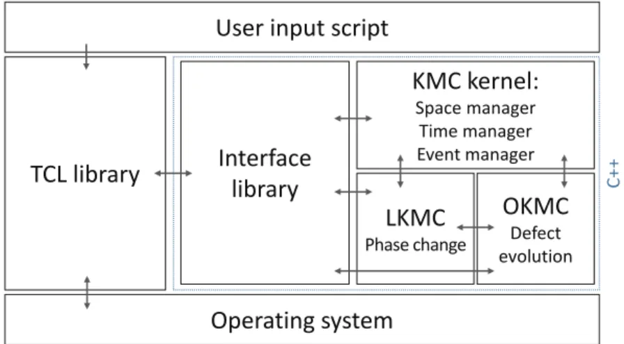
I.25 Structure of MMonCa, the KMC simulator used in this work . . . 26
II.1 Sketch of incomplete six-fold rings lying at the amorphous-crystalline inter-face. Amorphous atoms are coloured, crystalline ones in white. Highlighted bonds must be broken to recrystallise the whole six-fold ring . . . 33
II.2 Deciding tree for choosing the local configuration during SPER . . . 34
II.3 A {111} local configuration (a) and its twin defect (b) . . . 34
II.4 Simulation cells used to evaluate the substrate orientation dependence of the SPER rate. Only the (100) and (122) cells are presented, accounting for a ro-tation of θ = 0◦ and θ = 70◦ . . . 36
II.5 Comparison between experiments and LKMC simulation of the SPER rate dependency of the substrate orientation. Experimental data from [Csepregi
et al. 1978] and [Darby et al. 2013] . . . 37
II.6 The bond defect . . . 38
II.7 Distribution function of several amorphous phases generated with differ-ent bond defect concdiffer-entrations. Melt-quench generated amorphous phase is shown for comparison. Experimental data from [Laaziri et al. 1999] . . . 40
II.8 Bond angle distributions of several amorphous phases generated with differ-ent bond defect concdiffer-entrations. Melt-quench generated amorphous phase is shown for comparison . . . 40
II.9 Structure factor curves . . . 41
II.10 Schematic of the interface roughness interpretation. The cell is divided into subdivisions, where the α-c interface position is extracted, giving access to the average and standard deviation values of the interface position . . . 42
List of Figures ix
II.11 Simulation cell preparation for MD calculations. Views generated by OVITO [Stukowski 2010] 43
II.12 Plot of the extracted α-c interface vs. time for MD calculations of <100> silicon at 1800K. The resulting extracted SPER rate is shown . . . 44
II.13 Arrhenius plot of the SPER rates for the <100> silicon substrate orientation at MD temperatures. Extrapolations of experimental data from [Csepregi
et al. 1978], [Roth et al. 1990] and [Johnson & McCallum 2007] are plotted, as well as KMC and MD simulations results . . . 45
II.14 Arrhenius plot of the SPER rates for the <100> silicon substrate orienta-tion at process temperature. Extrapolaorienta-tions for MD simulaorienta-tions results are plotted. Experimental data from [Csepregi et al. 1978], [Roth et al. 1990] and [Johnson & McCallum 2007] . . . 45
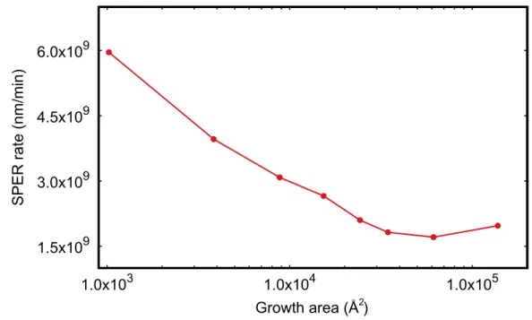
II.15 Molecular Dynamics extracted SPER rate on <111> substrate orientation for different cell sizes . . . 47
II.16 <110> view of cell during <111> SPER. Twin defects are invariably situated
after a few layers from the initial α-c interface (dotted line) for any growth area. Views generated by OVITO[Stukowski 2010] . . . 48
II.17 MD simulations of the α-c interface evolution over time for several temper-atures . . . 49
II.18 Molecular Dynamics SPER rate on <111> substrate orientation for different temperatures . . . 50
II.19 α-c interface evolution over time for a 1500K anneal . . . 51
II.20 State of the simulation cell after 141ns anneal at 1600K during a <110> substrate orientation MD calculation. The original α-c interface is plotted in dots. {111} interfaces are easily identifiable . . . 52
II.21 Molecular Dynamics SPER rate on <110> substrate orientation for differ-ent temperatures. Experimdiffer-ental data from [Csepregi et al. 1978, Drosd & Washburn 1982]. . . 53
III.1 Schematic of the possible reactions in the OKMC model: diffusion of a defect, binding of several defects and break-up of an extended defect . . . 61
III.2 Comparison between experimental data [Mirabella et al. 2008] and OKMC simulations for boron diffusion and clustering in amorphous silicon . . . 64
III.3 Convergence study on the update criterion to yield correct GFLS factor with a minimum computation impact for the cell size used in these investigations 67
III.4 Sketch of the amorphous-crystalline interface during SPER. As the BIC does not take place in SPER reaction, slow recrystallising <111> fronts appear around it. . . 68
x List of Figures
III.5 20 keV as implanted boron concentration profiles for two different doses and hole densities after 900◦C anneal during 10 s for two different implant doses. Experimental data from [Solmi et al. 1990]. The hashed part represents the boron inactivated by the clustering reaction . . . 69
III.6 SPER rate increases for a 500◦C anneal. Experimental data from [Park
et al. 1988, Gouy´e et al. 2010, Johnson et al. 2012]. GFLS 0 and GFLS 1 show the incremental refinement of the LKMC model . . . 70
III.7 SPER rate versus a boron profile at T=500◦C. Data from [Jeon et al. 1989]. The KMC model yields good agreement with experimental data for the SPER rate versus the boron concentration.. . . 71
III.8 Boron concentration profile used to investigate interface roughness in pres-ence of boron and the positions of the α-c interface where snapshots were taken . . . 72
III.9 2D cross-section views of atoms at the α-c interface at three different boron concentration levels. Views generated with Ovito [Stukowski 2010]. . . 72
III.10 Example of dopant redistribution during SPER. P profiles at different times are shown during a RTA at 350◦C. Original α-c interface at 220 nm. The free surface at 0 nm. Data from [Simoen et al. 2009] . . . 73
IV.1 SPER rates and activation energies in SiGe alloys . . . 80
IV.2 Two possible configurations for atom 1 to be recrystallised on a <110> interface: either with atom 2 or 3. As atom 2 or 3 can be different in an alloy, the configurations should yield different recrystallisation probabilities. Red atoms are amorphous, to be filled sites, and blue are crystalline. . . 81
IV.3 Schematic view of the simulation box used for SiGe SPER simulations. . . . 83
IV.4 Composition dependence of the recrystallisation rate during SiGe SPER at 450◦C. Experimental data from [Haynes et al. 1995] and [Kringhøj & Elli-man 1994] . . . 84
IV.5 Composition dependence of extracted activation energy for SiGe alloys SPER. The activation energy presents a maximum for Si60Ge40. Activation energies
extracted on limited temperature ranges are shown in dashed lines. Low tem-perature range: 300-450◦C. High temperature range: 450-650◦C. Solid line is the extraction on the whole temperature range. Experimental values from [Haynes et al. 1995] and [Kringhøj et al. 1995] . . . 84
IV.6 Experimental [Haynes et al. 1995, Kringhøj & Elliman 1994] and simulated SPER rates dependence on the germanium content on the main orientations during a 450◦C anneal. . . . . 88
List of Figures xi
IV.7 Available experimental [Csepregi et al. 1978,Darby et al. 2013] and simulated [Martin-Bragado 2012] normalized SPER rates dependence on substrate ori-entation during SiGe alloys recrystallisation . . . 88
IV.8 Cross-section of amorphous-crystalline interfaces after a 70 nm recrystalli-sation with the KMC model at 450◦C. Interface are faced up and shifted by 10 nm each to allow comparison. The SiGe alloys exhibit rough interfaces, particularly in the Ge-rich region. . . 89
IV.9 Bright-field cross-sectional TEM image of a SiGe 20% sample, grown on a graded buffer to avoid stress-related roughness, after a 70 nm recrystallisa-tion at 500◦C. . . 90
IV.10 Ratio of performed events during a M (100) recrystallisation. The local anisotropy brought by the competition between events leads to a rougher interface in Ge-rich alloys forcing more µ(110) recrystallisation events to be performed. This impacts the ratios between M (100) and M (110) SPER rates. . . . 91
IV.11 SiGe alloys lattice constants calculated at 300K with MD simulations. Ex-perimental data from [Dismukes et al. 1964]. . . 92
IV.12 <010> view of MD simulation cell states for different germanium concentra-tions after a 30 ns anneal at 1700K. Views generated by OVITO[Stukowski 2010] 92
IV.13 Interface evolution over time for several SiGe alloys by MD calculations . . . 93
IV.14 Extracted activation energies for SiGe alloys from several techniques: exper-imental data, LKMC model and MD calculations . . . 93
IV.15 Germanium concentration profiles at 0 ns and 30 ns during SiGe alloys SPER 94
V.1 TEM image of a SiGe layer epitaxially grown on silicon. Region 1 shows a highly defective layer with numerous threading dislocations due to the lattice mismatch. Region 2 is a relaxed SiGe layer. Adapted from [Harame et al. 2004]100
V.2 Schematic of the atomic scattering happening when X-rays are applied to a crystalline structure . . . 101
V.3 Schematic of Bragg’s law for diffraction in crystalline materials . . . 102
V.4 Scheme of the reciprocal space map of a cubic structure and a vector repre-sentation of the diffraction conditions in the reciprocal space . . . 102
V.5 Schematic showing the difference between strained and relaxed heteroepi-taxial layers . . . 103
V.6 Theoretical θ − 2θ curve using a (004) reflection converted in a Qz scan of a
SiGe layer epitaxially grown on a Si substrate . . . 104
V.7 Experimental installation for (004) HR-XRD carried out at the ESRF . . . . 104
V.8 θ-2θ curves converted in a Qz scan of SiGe layers after SPER with the highest
thermal budgets. Theoretical positions of the layer peaks for the strained and relaxed SiGe layers are shown . . . 106
xii List of Figures
V.9 Juxtaposed (004)RSMs of SiGe 22% and SiGe 42% showing partial relax-ation and total relaxrelax-ation. RSMs taken on samples with the highest thermal budget. RSM of SiGe 22% is shifted by -0.10 in Qx, allowing comparison . . 106
V.10 SiGe layer thickness evolution during the SPER of strained SiGe 12% with several temperatures . . . 109
V.11 SiGe layer thickness evolution during the SPER of strained SiGe 22% with several temperatures . . . 109
V.12 Schematic of the end of a layer recrystallisation in case of a rough interface. As some parts are still amorphous they will be recrystallised along <111> direction, slower than the [100] direction . . . 110
V.13 θ-2θ curves for SiGe 22% with the same layer thickness but different tem-peratures. Positions of the important Qz points are given . . . 110
V.14 (224)RSM for the sample SiGe 22% recrystallised at 460◦C . . . 112
V.15 (224)RSM for the sample SiGe 22% recrystallised at 540◦C . . . 112
V.16 Cross-section TEM images for SiGe layers recrystallised at 460◦C and 520◦C. Yellow lines symbolise the boundaries of the SiGe layer . . . 113
V.17 High-resolution cross-section TEM image showing hairpin dislocations in a recrystallised SiGe 22% layer . . . 113
V.18 Plan view TEM images for SiGe layers recrystallised at 460◦C and 520◦C.
Diffraction g vectors are given . . . 114
V.19 α-c interface roughness from MD simulations after 3 nm recrystallisation of strained SiGe 40% . . . 115
V.20 <100> views of MD simulations after 3 nm recrystallisation of strained SiGe 40%. The extracted average α-c interface position and their standard deviations are shown . . . 116
B.1 A single snapshot of the Maxipix 2D sensor. Regions of interest and the diffracted peak are shown . . . 129
B.2 (004)RSM resulting of a concatenation of transformation into reciprocal space of numerous snapshots during a XRD experiment. . . 130
B.3 Zoomed image of (004)RSMs before and after interpolation on a cartesian grid131
B.4 Interpolated (004)RSM. . . 132
List of Tables
I.1 Experimental extractions of the activation energy for pure silicon SPER . . 16
I.2 Experimental extractions of the activation energy for pure germanium SPER 17 II.1 Values used in the LKMC model . . . 35
II.2 Simulation and experimental extractions of the prefactors and activation energies in pure silicon SPER . . . 44
II.3 Cell sizes, growth areas and number of atoms. . . 46
II.4 The interpolation ranges and extracted SPER rates . . . 49
III.1 Defect reactions in amorphous silicon . . . 63
III.2 Point defect parameters for reaction in amorphous silicon . . . 63
III.3 Potential energies for Boron-Dangling bonds complexes in amorphous sili-con. Values from [Martin-Bragado & Zographos 2011] . . . 63
III.4 Point defect reactions in crystalline silicon . . . 64
III.5 Parameters used for binding and diffusion of point defects in crystalline silicon. Values from [Martin-Bragado et al. 2005] . . . 64
III.6 Defect energy level at T=0K for charge state transition in crystalline silicon. The valence band maximum is used as the reference. Values from [ Martin-Bragado et al. 2005] . . . 64
III.7 Defect reactions at the α-c interface during SPER . . . 65
IV.1 SPER activation energies for each chemical bond used in the model . . . . 82
IV.2 Local configuration prefactors for each chemical bond used in the model . . 82
V.1 Thermal budgets applied during HR-XRD experiments . . . 105
V.2 Activation energies for strained SiGe layer SPER . . . 108
V.3 Critical thicknesses for the layers used in this work derived from [Paine et al. 1990] for the emergence of strain relaxation phenomenon during SPER114 A.1 Formation energies for Boron-Interstitial complexes in crystalline silicon . . 127
Chapter I
Context and goals of this work
Contents
1 Technological context . . . 1
1.1 Devices scaling throughout the years . . . 1
1.2 New approach: 3D sequential integration . . . 3
1.3 New material: Silicon-germanium alloys . . . 6
1.4 The 3D sequential integration process and its challenges . . . 6
2 The amorphous to crystalline transition . . . 10
2.1 Phase structures. . . 10
2.2 Recrystallisation thermodynamics and kinetics. . . 14
2.3 Its numerous dependencies . . . 17
3 Simulation context: atomistic simulations . . . 20
3.1 Ab initio methods . . . 21
3.2 Molecular Dynamics methods . . . 22
3.3 Monte Carlo methods. . . 23
4 Scope and aim of this thesis . . . 25
5 French summary — R´esum´e . . . 26
1
Technological context
1.1
Devices scaling throughout the years
The semiconductor industry is in a steady evolution since the beginning of the electronic computer, the Electronic Numerical Integrator Analyser and Computer, or ENIAC, until now. These regular evolutions have been condensed into the now famous Moore’s law, stating that the density of transistor is relatively doubling every two years. The industry followed this trend until the middle of the 2010 decade, where the International Technology
2 Chapter I. Context and goals of this work
Roadmap for Semiconductors predicted a decrease in this trend1 and one of the industry
leader, Intel, has slowed down its research and development cycles as the device scale approach the 10 nm gate length2.
Another way to see the steady evolution of the semiconductor industry is introduced by Koomey et al. [Koomey et al. 2011]. In the publication, the team concludes that the number of computations per energy dissipated has been doubling around every 1.57 years. This trend, named Koomey’s law, has been surprisingly well followed since the beginning of electronic computers, as it can be seen in Figure I.1, contrary to the Moore’s law 3, which seems to slow down.
10-2 100 102 104 106 108 1010 1012 1014 1940 1950 1960 1970 1980 1990 2000 2010 2020
GFLOPS per Watt
Years
Figure I.1: Number of computations per joule dissipated. The Koomey’s law states that the efficiency doubles every 1.57 years. Data from [Koomey et al. 2011], [Dong et al. 2014] and the first CPU-only based supercomputer on the Green 500 list, the ZettaScaler-1.6
The industry is approaching the limits of the Complementary Metal Oxide Semicon-ductor (CMOS) technology in term of gate length. The advanced nodes below 20 nm are technically very challenging to process as several issues have been encountered, such as short channel effect, gate and junctions leakages. To overcome these issues, several architectures have been proposed. From bulk CMOS, planar Fully Depleted Silicon on Insulator (FDSOI), TriGate or FinFET architectures have been introduced to cope the aforementioned issues [Ferain et al. 2011] (seeFigure I.2). As an example, to increase the electrostatic control of the gate, two possibilities exist. First, from bulk CMOS, the in-troduction of a depleted silicon layer over an oxide in FDSOI structures greatly enhances the electrostatic control [Weber et al. 2008]. This method can be seen in Figure I.2a. Another way to increase this control is to create a larger contact area between the gate
1http://bit.ly/2jXtu2S
2
http://bit.ly/1LGd3ly
3
1. Technological context 3 Drain Source Gate Drain Source Buried Oxide Gate
Bulk device FDSOI device
(a) 2D sketches of bulk and FDSOI devices
Double Gate / FinFET TriGate Gate Oxide Fin Gate Gate Fin
(b) 2D sketches of FinFET and TriGate devices based on bulk base
(c) 3D sketches on FinFET (left) and TriGate (right) devices based on a FDSOI substrate. Adapted from [Ferain et al. 2011]
Figure I.2: The different CMOS transistor technologies
and the channel. Three dimensional transistors thus appeared. Sketches of these 3D transistors, either TriGate or FinFET are drawn in Figure I.2b. Ultimately, one of the best electrostatic control can be achieved by combining the two former methods. This results in 3D transistors with a FDSOI base as in Figure I.2c.
1.2
New approach: 3D sequential integration
The fact that the transistors are now very efficient, thus producing less heat, allowed a new approach to device scaling. It is indeed possible to stack transistors in order to virtually double the transistors density with the same footprint and thus continuing the Moore’s law. This technique is called 3D integration.
3D integration is usually invoked for a parallel 3D integration where two parts are pro-cessed separately and bonded together with Through Silicon Vias (TSV). This technology is used to improve integration density and lower interconnect delay and latency issues be-tween several circuits. A basic scheme of this technology is shown in Figure I.3.
However, this technique cannot be used to front-end processing with transistors as the alignment of the two wafers during bonding is not fine enough to allow high performances. A new approach to effectively double the transistor density and overcome the alignment issue has been introduced. The technique is called 3D sequential integration and consists of sequentially processing two layers of transistors and connect them in a last step. Both top and bottom transistors are based on the FDSOI architecture. The process integration
4 Chapter I. Context and goals of this work
scheme is summarised in Figure I.4.
a) Wafers separately processed
b) Stacking and bonding
Figure I.3: Parallel integration process flow: a) two wafers are separately processed and b) contacted afterwards
a) Bottom transistors processing b) Top transistors processing
c) Contacting
Figure I.4: 3D integration process flow: a) bottom transistors are processed, b) top transistors are processed, c) contacts are made
The 3D sequential integration technique possesses its own challenges in order to com-pete with the more traditional integration techniques, id est FinFET, TriGate or FDSOI integrations. Indeed, the allowed thermal budget for the top layer must be reduced to a minimum in order to keep the bottom transistor from any degradations. These degrada-tions, reduced salicide stability, gate oxide growth, dopant diffusion and deactivation, can severely hinder the performance of the bottom transistors [Batude et al. 2011a, Batude
et al. 2013]. A simple scheme of the 3D integration process can be seen in Figure I.5. First, the bottom transistor is processed with a conventional high temperature thermal budget. Secondly, a SOI substrate is bonded via a low temperature (200◦C) molecular bonding, thus allowing a full transfer of the crystalline layer. A Transmission Electron Microscopy (TEM) cross-section image of the process result [Batude et al. 2011b] can be seen in Figure I.6.
For the technological process considered in this work, several thermal budgets have been considered. Figure I.7 shows the thermal budgets (TB) that yield a stable FET. The maximal aimed thermal budget is therefore 500◦C-5h for the top layer. One of the challenge is to sufficiently activate the dopants with such a low thermal budget, particularly when it is compared with conventional ones that are around 1100◦C. It is
1. Technological context 5
Figure I.5: Description of the 3D integration process flow at the transistor level. The bottom transistor is processed with a high temperature budget, an interlayer is deposited and the top transistor is processed with a low temperature budget
Figure I.6: TEM images of two stacked transistors fabricated according to the 3D integration process [Brunet et al. 2016]
°
Figure I.7: Stable thermal budgets for FET fabrication using the CoolCubeTM integration [Batude et al. 2015]
6 Chapter I. Context and goals of this work
therefore not possible to use conventional process — rapid thermal anneal (RTA) — to activate the dopants. Fortunately, there are other processes that can activate dopants with a low thermal budget. Very short anneal enabled by dynamic surface anneal, an annealing technique using a nanosecond LASER, appears to be a promising candidate to activate the top transistor [Batude et al. 2015, Cristiano et al. 2016]. This technique uses a Liquid Phase Epitaxial Regrowth reaction or LPER, where the amorphous phase is liquefied using nanosecond LASER pulses but not the cristalline one.
The Solid Phase Epitaxial Regrowth (SPER) can also place doping atoms into the lattice sites, thus activating them, with a thermal budget in accordance with the limitations of 3D sequential integration. In the 3D integration, the top transistor is thus processed using SPER for dopant activation. Contrary to the LPER, both phases stay solid in the SPER reaction. After a SPER process, a very high concentration of electrically active dopants is achieved far above equilibrium [Solmi et al. 1990]. In this work, the latter option will be investigated.
1.3
New material: Silicon-germanium alloys
Along with the formerly introduced new architectures, silicon-germanium (SiGe) alloys have been considered by the semiconductor industry as a replacement of only silicon-based transistors, in order to furtherly increase transistor performance. This performance increase can be achieved in two ways. First, with a silicon channel, compressive strained SiGe source and drain increase the hole mobility in the channel, as in [Ghani et al. 2003]. Second, by growing directly a compressive SiGe alloy layer for the whole junction, source - channel -drain, as in [Cheng et al. 2012].
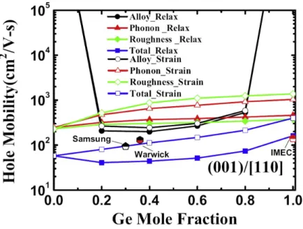
By compressively straining a Si, Ge or SiGe alloy channel, light and heavy bands split. Light holes are thus more populated and the hole mobility is increased. Moreover, as the germanium holes have lighter masses, the use of strained SiGe alloys, instead of only strained silicon, combines the performance boost of strain and germanium inclusions [Cheng et al. 2015]. The hole mobility incremental performance boost can be seen in
Figure I.8. Ultimately the device performances are boosted as it can be seen inFigure I.9. In the 3D sequential integration, a strained SiGe-based transistor is used, as it offers the best performances possible in conjunction with an FDSOI architecture.
1.4
The 3D sequential integration process and its challenges
The former sections introduced the architecture — FDSOI — and material — strained SiGe alloys — that are used within a 3D sequential integration. However, this integration raises numerous challenges. They will be presented in the following sections.
1. Technological context 7
Figure I.8: Hole mobility incremental performance boost by adding compressive strain and germanium. From [Cheng et al. 2015]
Figure I.9: Transistor performances increase due to inclusion of a compressively strained SiGe alloy channel. From [Cheng et al. 2012]
1.4.1 Strained SiGe layer manufacturing
The manufacturing of strained SiGe layer is rather difficult and could be the object of an entire chapter. The work presented here will not focus on this issue but will only highlight the difficulties of such a process.
SiGe alloys have their own lattice constants for each germanium concentration. The lattice constant can be roughly approximated by a linear interpolation as a function of the germanium content between the pure silicon lattice constant (5.43 ˚A) and the pure germanium one (5.66 ˚A). When epitaxially grown on a silicon substrate, the SiGe alloys has to match the lattice constant of the substrate, as it can be seen in Figure I.10. This
8 Chapter I. Context and goals of this work
results in a biaxially compressive strained SiGe layer.
aSi aSi0.7Ge0.3 aSi SiGe epitaxy Relaxed SiGe Relaxed Si Compressed SiGe layer a S i0.7 Ge 0.3
Figure I.10: Strained SiGe manufacturing by epitaxial growth on a relaxed silicon layer.
The strain resulting from the lattice mismatch is elastically stored in the grown layer and more grown thickness means more elastic energy. However, the grown thickness must be kept below a critical thickness to prevent the grown layer to relax via the formation of misfit dislocations. This issue has been thoroughly investigated in the following works [Matthews & Blakeslee 1974,People & Bean 1985,Paine et al. 1991,Hartmann et al. 2011].
In fine up to 40 nm SiGe layer containing up to 40% of germanium can be epitaxially
grown on a silicon substrate. These limits match with the 3D sequential integration requirements, where a layer with less than 30 nm is grown.
1.4.2 Amorphisation and SPER
A low thermal budget — fixed below 500◦C-5h — has been introduced in the transistor processes in order to stay within the constraints imposed by the 3D sequential integration process. The solid phase epitaxial regrowth verifies the 3D sequential constraints and activate the dopant. Dopant activation via SPER can be resumed into three steps. Firstly damage is created to a crystalline substrate for it to become amorphous, i.e a disordered phase. This step is called the pre-amorphisation implant (PAI). Secondly, the dopant is implanted. Finally, the substrate is annealed and the amorphous phase previously generated recovers its crystallinity, through the aforementioned SPER process. This step also places the dopant into the lattice positions, thus activating them and will be presented in the following section. Figure I.11 presents the two main steps in a) and b), where the PAI and dopant implantation are merged into step a). This is possible only in the case
1. Technological context 9
where the dopant has a high enough mass to amorphise the substrate. In the case of light atoms, such as boron, two implantations are made, one to amorphise the substrate and one to place the boron atoms.
Buried Oxide (BOX)
Figure I.11: Junction formation steps with SPER technique: a) source and drain are amorphised, b) the SPER reaction is activated by an anneal and subsequently activates the source and drain regions
Amorphous silicon or silicon-germanium layers can be achieved with high energy im-plantation into crystalline layers. Upon imim-plantation, each ion collides with lattice atoms and expels them from their lattice sites, thus creating interstitial and vacancy point de-fects. Each lattice atom that has been expelled possesses a kinetic energy given by the collision with the implanting ion. These expelled atoms can thus in turn collide with other lattice atom, creating successive collision events, called a cascade. Such an event can be seen in Figure I.12. During the implantation, the point defects may recombine if there is enough lattice vibration. This substrate healing, called dynamic annealing, is directly linked to the temperature during implantation. When the lattice is heavily damaged, it will reorganise itself into small amorphous pockets.
Incindetal ion
Figure I.12: Sketch of a single atomic collision and the resulting cascade. Vacancy and interstitial defects are the result of a single cascade
The amount of damage produced by the implantation is proportional to the mass, dose and energy of the incoming atoms. Higher masses and energies yield a higher inertia for the incoming atom, thus giving it a higher damage power. The dose, how many atoms are implanted by units of area, increases the probability of amorphisation of the volume.
10 Chapter I. Context and goals of this work
With high enough doses and dose rates, the small amorphous pockets grow large and finally form a continuous amorphous layer on top of the crystalline phase. These steps are sketched in Figure I.13.
Vacancy Interstitial
Ion implant
a) b) c)
Amorphous pockets
Figure I.13: Continuous cascades leading to a continuous amorphous layer
In the 3D sequential integration, the amorphisation process is challenging. Indeed, a non-damaged crystalline seed is required for the subsequent recrystallisation. As the transistor architecture is FDSOI with a material thickness below 30 nm, as it can be noted in Figure I.6, the amorphisation control is difficult. Too little amorphisation and the transistor will not perform well due to less active dopants. A too deep amorphisation and the device performs even worse as the single crystal is destroyed. Indeed, without a proper crystalline seed, the SPER cannot happen. In this particular case, Random Nucleation Growth (RNG) happens and yields a polycrystal. Due to its poor electrical performances, a polycrystal must be avoided with utmost importance, reinforcing the need of precision during PAI. The interested reader can consult [Spinella et al. 1998]. The differences between these reactions are highlighted in Figure I.14. The process window is therefore tiny. Fortunately, this window can be revealed with careful upstream preparation with atomistic simulations that have been consistent with experimental data on the whole SiGe alloy spectrum [Payet et al. 2016a].
2
The amorphous to crystalline transition
2.1
Phase structures
2.1.1 Crystalline siliconUnder pressure and temperature conditions encountered during semiconductor processes — from -3 to +3 GPa and below 1600K — the lowest energy phase of crystalline silicon (c-Si) is the diamond structure [Kaczmarski et al. 2005], as seen in Figure I.15a. The diamond structure is often described as an interlacing of two face-centred cubic system
2. The amorphous to crystalline transition 11
c-Si α-Si
α-Si agglomerates crystallites
a) SPER
b) RNG
Figure I.14: Sketch revealing the difference between a) SPER and b) random nucleation growth (RNG)
that are shifted between each other by one fourth of the lattice unit in [100], [010] and [001] orientation. The diamond structure can also be described as a Zincblende structure with a unique atom instead of a two-atom alternation, as it can be seen in Figure I.15a. In this structure, each silicon atom are covalently bonded with 4 other atoms. A single silicon atom has an electronic structure of [Ne]3s23p2, but in order to minimise the atom
total energy, 3s and 3p orbitals hybridise into a sp3 orbital. The covalent bonds form
therefore a regular tetrahedron with an angle of 109◦ between each bond.
The silicon unit cell contains 8 atoms, as seen in Figure I.15a, with a lattice parameter of
aSi=5.43072 ˚A at 300K [Pichler 2004], giving a concentration of 5×1022 cm−3. At room
temperature, the bond length between two atoms is aSi·
√
3/4 = 2.352 ˚A. Each silicon atom has 4 first neighbours at a distance of aSi·
√
3/4, 12 unique second neighbours at a distance of aSi·
√
2/2 and 12 unique third neighbours at a distance of aSi·
√
11/4. Two dimensional projections of the silicon lattice along [100], [110] and [111] can be seen in
Figure I.15b, Figure I.15c and Figure I.15d, respectively.
The structure of SiGe alloys is the same as pure silicon, as germanium and silicon atoms possess the same outer shell electronic configuration. However, the germanium atom is bigger and the alloy lattice constant can be approximated by the Vegard’s law. The Vegard’s law is an empirical rule stating that a linear relation exists, at constant temperature, between the crystal lattice constant of an alloy and the concentrations its pure elements. More precisely in the case of SiGe alloys, the Vegard’s law is not stricto
sensu followed as experimental data [Dismukes et al. 1964, Kasper et al. 1995] and first principle calculations [de Gironcoli et al. 1991] have shown.
12 Chapter I. Context and goals of this work
[100] [010]
[001]
(a) Three dimensional view (b) View in <100> direction
(c) View in <110> direction (d) View in <111> direction
2. The amorphous to crystalline transition 13
2.1.2 Amorphous silicon
The amorphous phase is often described as a continuous random network (CRN). The structure of amorphous silicon (α-Si)— or a SiGe alloy — shares some properties with the crystalline phase. Atoms are still covalently bond to four nearest neighbours with bond lengths that do not significantly differ between the two phases. In SiGe alloys as well as pure silicon or germanium, amorphous phases are always less dense (∼2%) than crys-talline ones [Custer et al. 1994, Laaziri et al. 1995]. Bond angles however deviate from the crystalline phase. Experimental data from high energy X-ray diffraction of amor-phous silicon present an average of the bond angle distortion (∆θ) between 9-10◦ [Laaziri
et al. 1999]. These two properties can be viewed with the partial distribution function
g(r) (PDF) comparison between the two phases. This function describes the probability
to find an atom at a given distance from the centre of another atom. Mathematically,
g(r) is defined as [Takeshi & Billinge 2012a]:
g(r) = 1 4N πr2ρ 0 X i,j δ r − |Ri − Rj| ! (I.1)
where N is the number of total atoms, ρ0 is the material density — here 0.049 at/˚A3
[Laaziri et al. 1995] — and |Ri− Rj| is the distance between atoms i and j. A high value
means the presence of atoms whereas a low value means a void. As a diamond lattice crystal is well ordered, neighbour peaks are easily identifiable. The PDF of amorphous and crystalline silicon can be seen at Figure I.16. Experimental data are derived from the radial distribution function R(r) (RDF) of [Laaziri et al. 1999]. The link between the PDF g(r) and the RDF R(r) is R(r) = 4πr2ρ0g(r) [Takeshi & Billinge 2012b].
Both phases share the same order at close range as one can see the first and second peaks that symbolize the first and second nearest neighbours presences. However, amor-phous silicon loses long range order as the function shows no more peaks after 4 ˚A. The bond length is also preserved as the first peak coincides between the two curves. Due to this loss of order, amorphous silicon or germanium possesses a lower melting point than their crystalline counterparts, as seen by [Donovan et al. 1985].
Furthermore, amorphous phases host several defects. The first defect experimentally seen was an undercoordinated atom, called the dangling bond defect, due to its detectability by the Electron Spin Resonance (ESR) method [Brodsky & Title 1969]. From ESR measure-ments, the concentration of dangling bonds in amorphous silicon is around 2 × 1020cm−3.
Later [Pantelides 1986] introduced an overcoordinated defect, called floating bond. Fi-nally, tight-binding approach confirmed the presence of neutral dangling bonds, positively and negatively charged dangling bonds and floating bonds in amorphous silicon [Knief & von Niessen 1999]. Contrary to the dangling bonds, floating bonds are not susceptible to
14 Chapter I. Context and goals of this work 0 2 4 6 8 10 12 14 16 18 20 0 2 4 6 8 10
Pair distribution function g(r)
r(Å)
Crystalline silicon Amorphous silicon
Figure I.16: Partial distribution function g(r) comparison between crystalline and amorphous silicon. The amorphous curve is derived from experimental work of [Laaziri et al. 1999]
the ESR method hence their concentration is not known.
2.2
Recrystallisation thermodynamics and kinetics
Due to this loss of its long-range order, the α-Si or α-Ge has a higher Gibbs free energy than its crystalline counterpart. The recrystallisation reaction is therefore thermody-namically favourable as the difference in Gibbs free energy between an amorphous and a crystalline atom, ∆Gαc≡ Gα− Gc, is positive. This free energy can be written:
∆Gαc(T ) = ∆Hαc(T ) − T ∆Sαc(T ), (I.2)
where ∆Hαc and ∆Sαc are the recrystallisation enthalpy and entropy, respectively.
En-thalpies and entropies can be extracted via Differential Scanning Calorimetry (DSC) by determining the specific heat capacity of the recrystallisation. Donovan et al. [Donovan
et al. 1985] determined a crystallization enthalpy of 11.9 ± 0.7 kJ/mol (at 960 K) and 11.6 ± 0.7 kJ/mol (at 750 K) for silicon and germanium respectively of ion-implantation generated amorphous layers.
The amorphous to crystalline transition has been established as thermodynamically favourable reaction. However, the reaction has to be thermally activated, as it can be seen in Figure I.17. This graphical representation shows that even if the reaction is thermodynamically favourable (∆Gαc> 0), an energetic barrier ∆G∗ has to be overcome.
The growth rate of the recrystallisation or the rate of the moving amorphous-crystalline interface, can be written [Olson & Roth 1988,Lu et al. 1991], within the Transition State
2. The amorphous to crystalline transition 15 α Si Si G* Gαc Recrystallisa on E n e rgy (eV )
Figure I.17: Energetic representation of the SPER reaction
Theory of thermally activated growth [Christian 1965]:
v = kBT h f λ 1 − exp − ∆Gαc kBT ! × exp − ∆G∗ kBT ! (I.3)
where kBT /h is the lattice vibration frequency, f is the fraction of sites where the atomic
rearrangement can occur, λ is the distance that the interface moves during a unique re-arrangement. Finally, ∆G∗ is the SPER activation free energy.
∆G∗ ≡ ∆H∗− T ∆S∗, where ∆H∗ is the activation enthalpy and ∆S∗ is the activation
entropy. Furthermore, within the framework of the transition state theory for a bimolec-ular reaction, the relationship between the activation energy and the activation enthalpy can be written as follow [Atkins 2009]:
E∗ = ∆H∗+ kBT (I.4)
Moreover, in the case of the SPER reaction, ∆H∗ kBT , yielding ∆G∗ ∼= E∗− T ∆S∗.
The Equation I.3 can now be rewritten:
v = v0× exp − ∆E∗ kBT ! (I.5) With v0 v0 = kBT h f λ 1 − exp − ∆Gαc kBT ! × exp ∆S∗ kB ! (I.6)
At 600 ◦C, 0.137 < ∆Gαc < 0.217eV [Donovan et al. 1985, Roorda et al. 1991] thus
16 Chapter I. Context and goals of this work
Equation I.5 can be rewritten under the form of an Arrhenius equation [Arrhenius 1889]
v = A × exp(−E∗/kBT ). The activation energy for the SPER reaction can be extracted
via temperature dependent experiments with E∗ ≡ −kB∂(log v)/∂(T−1). Examples are
given in Figure I.18 where the regrowth rates of silicon on several substrate orientations are plotted. The regrowth rate is extracted by measuring the α-c position over time. Two main experimental techniques are used, either Rutherford Backscattering Spectrometry (RBS) or in situ Time Resolved Reflectometry (TRR). Several authors have extracted the activation energy for pure silicon SPER, as seen in Table I.1. The activation energy for pure silicon SPER is now widely admitted to be 2.7 eV. For germanium, similar experiments have been done, with results are compiled inTable I.2. For pure germanium, the value of 2.17 eV is widely used. Finally, the case of SiGe alloys will be introduced later in this work.
Reference Temperature range (◦C) E∗ (eV) [Csepregi et al. 1978] 450-575 2.35 ± 0.1 [Olson & Roth 1988] 500-1000 2.68 ± 0.05
[Roth et al. 1990] 500-750 2.70 ± 0.02
[McCallum 1996] 480-660 2.7
Table I.1: Experimental extractions of the activation energy for pure silicon SPER
10-2 10-1 100 101 102 103 104 0.95 1 1.05 1.1 1.15 1.2 1.25 1.3 1.35 1.4 750 800 850 900 950 1000 1050
SPER rate (nm/min)
103/T (K-1) Temperature (K)
(100) Csepregi et al. (100) Roth et al. (100) Johnson & McCallum (110) Csepregi et al. (111) Csepregi et al.
Figure I.18: Arrhenius plot of the SPER rate of silicon on three substrate orientations. Data from [Csepregi et al. 1978], [Roth et al. 1990] and [Johnson & McCallum 2007]
2. The amorphous to crystalline transition 17
Reference Temperature range (◦C) E∗ (eV)
[Csepregi et al. 1977b] 310–370 2.0
[Donovan et al. 1985] 417–457 2.17
[Lu et al. 1991] 300-365 2.17 ± 0.2
[Kringhøj & Elliman 1994] 290-430 2.02 ± 0.015
[Haynes et al. 1995] 290-390 2.19 ± 0.02
[Johnson et al. 2008] 300-540 2.15 ± 0.04
[Claverie et al. 2010] 300-540 2.16
Table I.2: Experimental extractions of the activation energy for pure germanium SPER
2.3
Its numerous dependencies
2.3.1 Substrate orientationAs it can be seen in Figure I.18, the silicon regrowth rates differ upon the substrate ori-entation. Measurements of the regrowth rate along different orientations confirmed this trend, as seen in Figure I.19. The SPER rate heavily depends on the substrate orienta-tion on silicon [Csepregi et al. 1978] and germanium [Darby et al. 2013]. However, even with these changes of the SPER rate, the activation energy is still 2.7 eV for silicon. The orientation impacts only the pre-exponential factor of the Arrhenius equation [Csepregi
et al. 1978].
To understand this phenomenon, Csepregi et al. suggested that the layer-by-layer recrys-tallisation occurs at kink sites on <110> ledges on {111} orientations terraces [Csepregi
et al. 1978]. The substrate orientation dependence thus comes from the density of <110> available ledges. Furthermore, Spaepen [Spaepen 1978] noted that the recristallisation mechanism involves a bond that has to be broken. Finally, these two concepts were re-fined in a model based on the bond density that are available to be broken at the α-c interface [Custer 1992]. The model of Custer yields very good agreement with the sub-strate orientation dependence of silicon, as it is shown in Figure I.19.
This bond breaking model has been reviewed as the most propable mechanism [Aziz 1992] amongst other proposed mechanisms for SPER. The model relies on the generation of dangling bonds at the α-c interface caused by breaking a bond. The dangling bonds furthermore migrate along the interface and reconstruct it along their way.
2.3.2 Hydrostatic pressure and non-hydrostatic stress
In the previous section, the SPER rate has been shown to follow an Arrhenius behaviour, in Equation I.3with an energy barrier of ∆G∗ furtherly reduced to an activation energy.
However, if we fully expand the Gibbs free-energy, it yields:
18 Chapter I. Context and goals of this work 0 0.2 0.4 0.6 0.8 1 0 10 20 30 40 50 60 70 80 90
SPER rate (normalized to (100) rate)
Angle (o) Si Csepregi et al.
Ge Darby et al. Si model Custer
Figure I.19: Regrowth rates for silicon and germanium SPER showing their substrate orientation dependences. Experimental data from [Csepregi et al. 1978] and [Darby et al. 2013]. Model from [Custer 1992]
where ∆E∗ is the activation energy, ∆S∗ the entropy change and ∆V∗ the volume change upon recrystallisation. The SPER thus have also a pressure dependence. Using the same approximations as before, Equation I.5 becomes:
v = v0× exp −
∆E∗+ P ∆V∗
kBT
!
(I.8)
∆V∗ is also called activation volume to parallel the activation energy. This activa-tion volume can be extracted during an isothermal pressure-dependent experiment with ∆V∗ = −kBT ∂(log v)/∂P . Lu et al. [Lu et al. 1991] measured an exponential
in-crease of the SPER rate with the hydrostatic pressure, giving a negative activation vol-ume. They extracted ∆V∗ = −0.28 ± 0.03ΩSi with ΩSi = 12.1cm3/mol for silicon and
∆V∗ = −0.46Ω
Ge with ΩGe= 13.6cm3/mol.
Aziz et al. [Aziz et al. 1991] expanded the notion of activation volume for non-hydrostatic pressure by introducing a second order tensor: ∆Vij∗. Assuming that the SPER reaction is bounded by a single process and extending the transition state theory a non-hydrostatic stress represented by a second order strain tensor σij yields:
v(σ) = v(σ = 0) × exp σij∆V ∗ ij kBT ! (I.9)
The activation volume is therefore extended to an activation strain tensor ∆Vij∗. Aziz et al. conducted experiments on silicon <100> SPER with an in–plane uniaxial stress over the range of ±600MPa. Their results show a SPER rate decrease with a tensile uniaxial stress and an increase with a compressive uniaxial stress. More recent experiments conducted by Rudawski et al. [Rudawski et al. 2008] on silicon <100> SPER with an extended
2. The amorphous to crystalline transition 19
range (±1.5GPa) show a decrease with tensile stress but no increase with compressive stress. This behaviour of the SPER rate regarding an uniaxial stress has been previously modelled into a Kinetic Monte Carlo model by Skl´enard et al. [Skl´enard et al. 2013]. The model states that the SPER reaction can be divided into two parts. First is a nucleation of an island and second its growth along <110> ledges. The SPER reaction can therefore be seen as a Frank–van der Merwe epitaxial growth mode. Under tensile or compressive stress, the nucleation rate is insignificantly change. However, the ledge recrystallisation rate is severely hindered under compressive stress whereas not hindered under tensile stress. Further details of the model and its implementation can be found in [Skl´enard
et al. 2013]. The model as well as the experimental data from Rudawski et al. are shown in Figure I.20.
Figure I.20: SPER rates under uniaxial stresses, [Rudawski et al. 2008] results and [Skl´enard
et al. 2013]’s model
2.3.3 Impurities
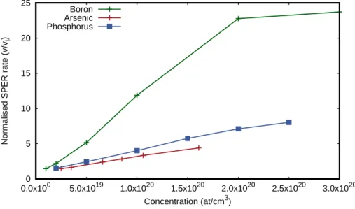
In the 3D integration structures, the SPER process aims to improve the dopant activation. SPER rate is strongly enhanced in presence of dopants. Csepregi et al. have seen that group III and V atoms implanted into <100> silicon tremendously enhances the SPER rate. The enhancement is dependent on the atom used, as it can be seen in Figure I.21.
This trend has been confirmed within numerous others investigations [Olson & Roth 1988,
McCallum 1999,Johnson & McCallum 2004]. However, at high concentration, the dopant can be pushed towards the surface during the SPER. This phenomenon called snow plough has been observed during arsenic SPER [Hopstaken et al. 2004,Demenev et al. 2012] and fluorine too [Mastromatteo et al. 2010]. High boron concentration does not lead to dopant redistribution. However [Gouy´e et al. 2010] has experience a limit to the SPER rate in-crease due to doping. Indeed, above 3×10²⁰ /cm3 boron concentration, the SPER rate
20 Chapter I. Context and goals of this work 0 5 10 15 20 25 0.0x100 5.0x10¹⁹ 1.0x10²⁰ 1.5x10²⁰ 2.0x10²⁰ 2.5x10²⁰ 3.0x10²⁰
Normalised SPER rate (v/v
i ) Concentration (at/cm3) Boron Arsenic Phosphorus
Figure I.21: SPER rate enhancement regarding several doping impurities, data from [Johnson & McCallum 2007]
does not increase anymore. Finally, aluminium and carbon, nitrogen or oxygen are known to decrease the SPER rate, even at moderate concentrations (< 1 × 10²⁰ at./cm3) [ John-son & McCallum 2007,Chevacharoenkul et al. 1991, Strane et al. 1996, Narayan 1982]. Lietoila et al. co-implanted both group III and V atoms at the same concentration and investigated the impact of this co-implantation during silicon SPER [Lietoila et al. 1982]. The co-implantation shows no SPER increase thus affirming that an electrostatic influ-ence is the cause of the SPER enhancement with doping impurities.
A model for the impact of doping impurities on the SPER rate has been developped and refined [Williams & Elliman 1983, Lu et al. 1991, Johnson & McCallum 2007, Johnson
et al. 2012]. This model is based on the assumption that the SPER rate is proportional to the concentration of defects responsible for the SPER. This defect concentration is also proportional to the Fermi level. As the substitutional doping impurities shift the Fermi level, the defect concentration will increase thus increasing the SPER rate. This model, called Generalised Fermi Level Shifting (GFLS), will be presented in-depth in chapter III. The interesting case of the germanium concentration influence during SiGe alloys SPER will be in-depth studied in chapter IV.
3
Simulation context: atomistic simulations
Technology Computer Aided Design (TCAD) is a division of Electronic Design Automa-tion aimed to model and simulate all aspects of a device fabricaAutoma-tion. This includes the modelling of process fabrication of a transistor, to the behaviour of several logic gates together. In the front-end processing of transistors, TCAD simulations are used in order
3. Simulation context: atomistic simulations 21
to simulate the process steps of the junction formation. The goal is to know the character-istics, such as defect concentration, dopant activation, stress distribution, of the junction for a specific parameter set and thus find the fittest set of parameters.
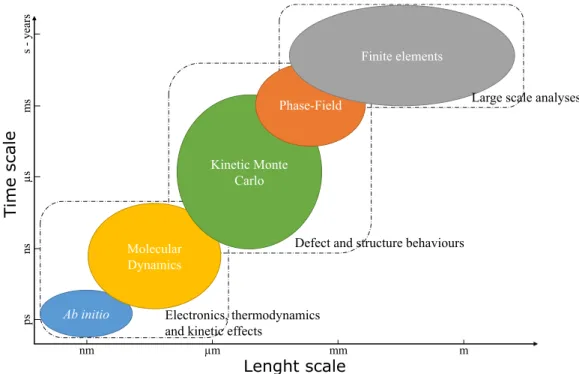
TCAD tools span over several timescales and length scales, as it can be seen inFigure I.22. Continuum models, sets of differential equations, can model macroscopic behaviours for large scales. However they lack the physical comprehension of the underlying mechanism generating the behaviour. Atomistic models compromise the simulation scales for a bet-ter grasp of the mechanisms occurring during the reaction. Atomistic simulations can be sorted into three different classes that will be explained in the following sections.
Lenght scale
Time scal
e
Figure I.22: Time and length scales of the several modelling possibilities and their respective application fields
3.1
Ab initio methods
Ab initio methods are non-empirical quantum mechanical methods used to investigate the
fundamental properties of materials. These methods use the full Schr¨odinger equation to investigate many-body systems. However, several approximations have to be introduced in order to be able to solve the Schr¨odinger equation.
As the ab initio methods are more often used to compute material properties of forma-tion energies, the Schr¨odinger equation can be written within time-independent, non-relativistic Born-Oppenheimer approximation:
22 Chapter I. Context and goals of this work
where T is the kinetic energy, Vext the external potential seen by the electrons and U
the electron-electron interaction. H is the Hamiltonian of the structure and Ψ its wave function.
There are numerous ways to define the wave function of a system. The simplest one is the Hartree-Fock method. However this method needs a huge computational effort. The wave function computation has been greatly simplified by the Hohenberg & Kohn theorem that states that the electron density is sufficient to describe the fundamental state of the system [Hohenberg & Kohn 1964]. This method is called the Density Functional Theory, or DFT, and has been widely used in materials science to investigate the ground state of a system. From the ground state of between several systems, formation energies of a certain defect can be deducted. Ab initio simulations are usually done with cells containing less than 1000 atoms and require large amount of computational time. However, they allow in-depth analyses of material properties.
3.2
Molecular Dynamics methods
Molecular dynamics (MD) method is a deterministic computer simulation used for in-vestigating the movement of vast numbers of particles. The molecular dynamics method can be used to investigate the motion of a system towards its lowest free energy state. The method originates from the late 1950s [Alder & Wainwright 1959]. The position and movement of an atom i in a system containing n atoms are governed by the Newton’s equations of motion:
mi
d2r
i
dt2 = Fi(r1, r2, ..., rn) (I.11)
where mi is the mass of the atom i, ri its position and Fi the forces upon it.
The force Fi computation is done with an interatomic potential. Several types of
poten-tial can be used, depending on the reaction and accuracy wanted. For example, when electron density of states or excited states are needed, potentials derived from ab initio methods are to be used but are extremely computationally demanding. Empirical poten-tial alleviate the computation costs but are bounded to certain atom type and must be carefully adjusted. For silicon SPER MD calculations, several many-body potentials can be used: Tersoff [Tersoff 1989], Environment Dependent Interatomic Potential (EDIP) [Bazant & Kaxiras 1996,Bazant et al. 1997,Justo et al. 1998], Stillinger-Weber [Stillinger & Weber 1985] or the Bond Order Potential (BOP) [Gillespie et al. 2007].
Figure I.23 succintly presents the algorithm for MD calculations. At the beginning, the atoms positions and velocities are initialised. Then the forces applied to each atom are calculated and the new atomic positions and velocities are calculated according the Newton’s equation. This step can be solved using the Verlet integration [Verlet 1967]. This loops is repeated until a certain time limit.
3. Simulation context: atomistic simulations 23
Figure I.23: Flow chart of the Molecular Dynamics algorithm
For silicon Molecular Dynamics, cells containing less than 50000 atoms have been used and the simulated time rarely exceeds 50 ns. This atomistic simulation method computational cost is directly linked to number of atoms in the cells and the simulated time. For the numbers discussed before, a simulation can be run below 10000 hours. Compared to
ab initio simulations, molecular dynamics ones can give insights on the kinetic effects
during reactions but at the cost of the loss of some intrinsic properties. For example, using the Tersoff potential during a MD simulation, the melting point temperature for silicon is found around 2400 K [Marqu´es et al. 2001], well above the value found in the experiments, 1685 K [Mayer & Lau 1990]. This method is unfortunately unsuitable to compute processes applied on a whole transistor.
3.3
Monte Carlo methods
The Monte Carlo method is a group of algorithms that is broadly used to solve problems in several fields, Mathematics and Physics, among others. The Monte Carlo method was developed by Metropolis & Ulam [Metropolis & Ulam 1949] in the end of the 40’s decade to investigate thermonuclear related problems. The name, Monte Carlo, comes from an area in Monaco famous for its casinos. The core idea of a Monte Carlo method is to solve a problem via a large set of random numbers, hence the relation with casinos. Although


![Figure I.24: Flow chart of the Bortz, Kalos and Liebowitz algorithm [Bortz et al. 1975] for Kinetic Monte Carlo simulations](https://thumb-eu.123doks.com/thumbv2/123doknet/12889559.370554/42.892.291.602.107.716/figure-bortz-kalos-liebowitz-algorithm-bortz-kinetic-simulations.webp)