1
Supporting Information
An Ultracompact GRIN-Lens-Based Spot Size Converter using Subwavelength Grating Metamaterials
José Manuel Luque-González,1* Robert Halir1, J. Gonzalo Wangüemert-Pérez,1 José
De-Oliva-Rubio1, Jens H. Schmid2, Pavel Cheben2, Íñigo Molina-Fernández,1 and Alejandro
Ortega-Moñux1
Mr. J. M. Luque-González, Dr. R. Halir, Prof. J. G. Wangüemert-Pérez, Dr. J. De-Oliva-Rubio, Prof. Í. Molina-Fernández and Dr. A. Ortega-Moñux.
1Universidad de Málaga, Dept. de Ingeniería de Comunicaciones, ETSI Telecomunicación,
Campus de Teatinos s/n, 29010 Málaga, España E-mail: [email protected]
Dr. J. H. Schmid and Dr. P. Cheben
2National Research Council Canada, 1200 Montreal Road, Bldg. M50, Ottawa K1A 0R6,
Canada
Abstract
We provide supporting information on the behavior of the proposed GRIN metamaterial when it is fed by TM polarized input light, a theoretical discussion about the normalized expansion ratio and alternative designs for silicon thicknesses of 250 nm and 300 nm.
1. Behavior of the GRIN metamaterial SWG structure for the TM polarization
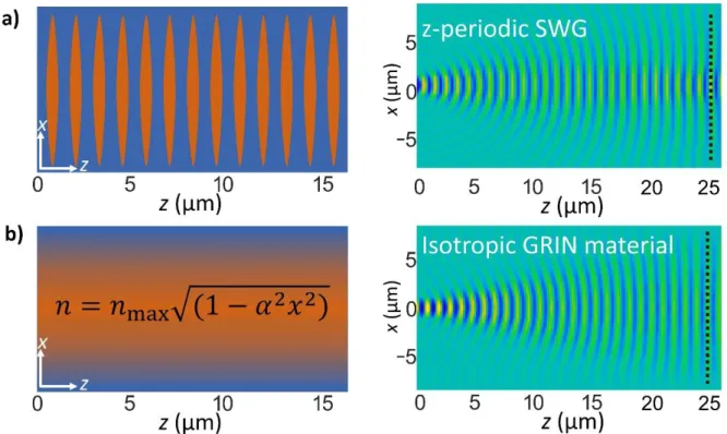
In the main manuscript we show that the GRIN metamaterial works as a spot size converter for TE polarization with anisotropy playing a key role in reducing the device length. Here we discuss, by using 3D-FDTD simulations, the behavior of the GRIN metamaterial for TM polarization. In Figure S1(a) we show the real part of the simulated TM electric field. Then, we propagate the same TM input field along an isotropic GRIN material [see Fig. S1(b)]. By comparing these two propagations it is apparent that the structure is behaving as an isotropic GRIN metamaterial. This result is expected since in a z-periodic SWG structure the anisotropy affecting the TM modes is negligible compared with the TE modes[S1]. In this device, for the TE polarization we require about 11 μm to achieve the desired expansion, while for TM
2
polarization about 24 μm are required. Thus, the main consequence of the isotropic nature of the metamaterial for TM modes is the longer collimation distance.
2. Normalized expansion ratio in anisotropic media
We use the normalized expansion ratio (NER) to compare different state-of-the-art spot size converters. The NER is defined as[S2]:
𝑁𝐸𝑅(𝜆) =𝑤𝑜𝑢𝑡/𝑤𝑖𝑛
𝐿/𝜆 · 𝐼𝐿(𝜆) = 𝐸𝑅̅̅̅̅ · 𝐼𝐿(𝜆), (S. 1)
where 𝑤out and 𝑤in are the widths of the output and input waveguides, L is the length of the spot size converter, λ is the vacuum wavelength of the propagating light and IL are the insertion losses (in linear scale). This parameter can be interpreted as an expansion ratio (𝐸𝑅 = 𝑤𝑜𝑢𝑡/𝑤𝑖𝑛), normalized by the electrical length of the device (𝐿/𝜆), and by the insertion losses of the device 𝐼𝐿(𝜆) = 𝑃𝑜𝑢𝑡(𝜆)/𝑃𝑖𝑛(𝜆). While insertion losses are highly implementation specific and thus difficult to treat analytically, the expansion ratio is more amenable to such a treatment. In the following we present and analytic estimation of the maximum value of 𝐸𝑅̅̅̅̅ =
𝐸𝑅
𝐿/𝜆 by using the well-known gaussian beam propagation formulas for isotropic and anisotropic media.
The width expansion of a gaussian beam propagating through a homogeneous isotropic material can be calculated as[S3]
𝑊(𝑧) ≈ 𝜃0· 𝑧, (S.2) 𝜃0 =𝜋·𝑊(0)𝜆 𝑛⁄ , (S.3)
where 𝑊(𝑧) is the beam radius at a distance z, 𝜃0 is the divergence cone half-angle, λ is the free-space operating wavelength, n is the refractive index of the material and 𝑊(0)is the beam radius at z=0.
The above expressions can be used to evaluate the (ER̅̅̅̅) of a gaussian beam propagating through an isotropic medium, thus obtaining:
ER
̅̅̅̅ =𝑤𝑜𝑢𝑡/𝑤𝑖𝑛
𝐿/𝜆 =
4 · 𝜆2
3
where the beam spot-sizes have been approximated as 𝑤in ≈ 2𝑊(0) and, 𝑤out≈ 2𝑊(𝐿). The beam spread can be even larger if the medium is anisotropic. In this case, the divergence half-angle can be calculated as[S4] 𝜃0 =𝜋·𝑊(0)𝜆 𝑛𝑛𝑥𝑥
𝑧𝑧
2 . The ER̅̅̅̅ of the gaussian beam propagating
through an anisotropic material is then ER ̅̅̅̅ =𝑤𝑜𝑢𝑡/𝑤𝑖𝑛 𝐿/𝜆 = 4 · 𝜆2 𝜋 ⋅ 𝑤𝑖𝑛2 𝑛𝑥𝑥 𝑛𝑧𝑧2 (S. 5)
It should be noticed that, for an isotropic medium, 𝑛𝑥𝑥 = 𝑛𝑧𝑧 = 𝑛, thus obtaining (S.4). Although a gaussian beam diffracting in a homogeneous medium does not exhibit a plane phase front, it provides a reference to compare with the expansion ratios of integrated beam expanders. We propose to use (S.5) as an estimation of the upper limit for the maximum normalized expansion ratio that can be obtained with a beam expander of length L.
Considering an initial beam width 𝑤𝑖𝑛 = 0.5 μm, an operating wavelength 𝜆 = 1.55 μm, and an isotropic material with refractive index 𝑛 = 2.85 (equivalent index for a silicon thickness hcore = 220 nm and TE polarization), we obtain ER̅̅̅̅ <∼ 4.3. All the designs included in Table 1 of the main manuscript exhibit NER values below this limit. Note that we assume no insertion losses in this upper limit. For the same silicon thickness, an anisotropic SWG metamaterial with a duty cycle DC = 50%, gives 𝑛𝑥𝑥 ∼ 2.26 and 𝑛𝑧𝑧 ∼ 1.82. Substituting these values in eq. (S.5) we obtain ER̅̅̅̅ <∼ 8.4. Note that this value should be normalized by the insertion losses of the spot size converter to calculate the NER.
3. SWG GRIN metamaterial for other silicon thickness
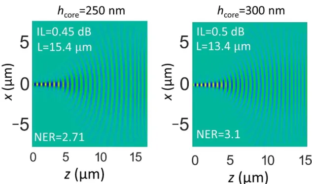
The proposed methodology to implement an anisotropic gradual index metamaterial is demonstrated in the main manuscript for a silicon thickness of 220 nm. In this section we reinforce the generality of this methodology by performing two additional GRIN lens spot size converter designs for the 250 nm and the 300 nm silicon thickness platforms. The design process of these lenses follows the one’s described in the manuscript: i) We calculate the look-up table with the duty-cycles that synthesize the desired GRIN metamaterial. ii) We simulate
4
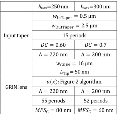
this metamaterial using a GRIN anisotropic homogenized structure in order to find the optimum value for the period and the minimum feature size. iii) We slightly refine the length of the device by using 3D-FDTD simulation arriving at the final dimensions shown in table S1 for the 250nm and 300nm silicon thicknesses. The field profile expansion for both GRIN lenses is shown in Figure 2S. In both cases (250 nm and 300 nm silicon thickness) the insertion losses of the device are below 1 dB and the NER is 2.71 and 3.1 respectively. Note that for the 300 nm silicon thickness the minimum feature size has been slightly decreased to 60 nm in order to achieve a good design.
5 References
[S1] J. M. Luque-González, A. Herrero-Bermello, A. Ortega-Moñux, Í. Molina-Fernández, A. V. Velasco, P. Cheben, J. H. Schmid, S. Wang, and R. Halir, Opt. Lett. 43, 4691 (2018). [S2] S. Abbaslou, R. Gatdula, M. Lu, A. Stein, and W. Jiang, Opt. Lett. 42, 4383–4386 (2017).
[S3] B. E. A. Saleh, and M. C. Teich, Fundamentals of Photonics (John Wiley & Sons, Inc., New York, USA, 1991).
[S4] D. D. Bhawalkar, A. M. Goncharenko, and R. C. Smith, Br. J. Appl. Phys. 18, 1431– 1441 (1967).
6
Figure S1. Schematic of the structure (left) and real part of the 3D-FDTD simulated main component of the electric field propagation for a TM polarized input field, ℛ𝑒{𝐸𝑦(𝑥, 𝑧)}, along the proposed GRIN lens (right) implemented with a) a z-periodic SWG structure, b) a gradual isotropic material.
7
Figure S2. Real part of the 3D-FDTD simulated main component of the TE electric field propagation, ℛ𝑒{𝐸𝑥(𝑥, 𝑧)}, along the proposed GRIN lens for a silicon thickness of a) hcore = 250 nm and b) hcore = 300 nm.
8 hcore=250 nm hcore=300 nm Input taper 𝑤InTaper = 0.5 μm 𝑤OutTaper = 2.5 μm 15 periods 𝐷𝐶 = 0.60 𝐷𝐶 = 0.7 Λ = 220 nm Λ = 200 nm GRIN lens 𝑤GRIN= 16 μm 𝐿Tip= 50 nm 𝑎(𝑥): Figure 2 algorithm. Λ = 220 nm Λ = 200 nm 55 periods 52 periods 𝑀𝐹𝑆C = 80 nm 𝑀𝐹𝑆C = 60 nm
Table S1. Geometrical parameters of the proposed spot size converters for the 250 nm and 300 nm silicon platforms.