Analysis of Variation in On-Chip Waveguide
Distribution Schemes and Optical Receiver Circuits
By
Karthik Balakrishnan
B.S., Computer Engineering
Georgia Institute of Technology, 2004
Submitted to the Department of Electrical Engineering and Computer Science in partial fulfillment of the requirements for the degree of
Master of Science in Electrical Engineering and Computer Science at the
MASSACHUSETTS INSTITUTE OF TECHNOLOGY May 22, 2006
0 Massachusetts Institute of Technology, 2006. All Rights Reserved
Author
Electrical Engineering and Computer Science May 22, 2006
Certified by
Duane S. Boning Professor of Electrical Engineering and Computer Science ~ . pervisor
Accepted by_
Smith
Chairman, Department Committee on Gradulte Studies Electrical Engineering and Computer ScienceMASSACHUSETTS INSTITUTE OF TECHNOLOGY
Analysis of Variation in On-Chip Waveguide
Distribution Schemes and Optical Receiver Circuits
By
Karthik Balakrishnan
Submitted to theDepartment of Electrical Engineering and Computer Science May 22, 2006
In Partial Fulfillment of the Requirements for the Degree of Master of Engineering in Electrical Engineering and Computer Science
ABSTRACT
Recently, optical interconnect has emerged as a possible alternative to electrical interconnect at chip-to-chip and on-chip length scales because of its potential to overcome power, delay, and bandwidth limitations of traditional electrical interconnect. This thesis examines the issues of variation involved in the implementation of a robust on-chip optical signal distribution network. First, the variation within the on-chip waveguide network is analyzed in terms of susceptibility to lithographic uncertainties and refractive index variations. Then, the robustness of an ultrashort pulse-based receiver circuit architecture is analyzed. Some variation sources considered are optical input power variation, load capacitance variation, parasitic capacitive coupling, and power supply noise. Simulation results show that, for both the passive waveguide network and the optical receiver circuit, variation can result in clock skew and jitter, which limit the frequencies at which the distribution network can operate.
The impact of technology scaling on the optical receiver circuit architecture is assessed with respect to variation. The robustness of the optical network is compared with that of an all-electrical signal distribution network. Results indicate, for the optical signal distribution network, that a trade-off exists between power consumption and robustness towards most sources of variation. In addition, the ultrashort pulse-based receiver circuit design demonstrates robustness towards many variation sources in the presence of technology scaling. The existence of variation in reasonable amounts will not obstruct the functionality of the receiver circuit. However, additional measures must be taken to minimize power supply variation and parasitic capacitive coupling, which will have a greater impact on robustness in future technology nodes.
Thesis Supervisor: Duane S. Boning
Acknowledgements
I would first like to thank my advisor, Duane Boning, for giving me the opportunity
to conduct research in his group and providing guidance to me numerous times along the way. This work would not have been possible without his help. I also want to thank all of my colleagues in the Statistical Metrology Group. Special thanks to Shawn Staker, Karen Gettings, Mehdi Gazor, Daihyun Lim, Nigel Drego, Kwaku Abrokwah, Xiaolin Xie, who have all helped me at some point or another along the way with my work. All of you have helped to create a vibrant atmosphere which has made the past few years here enjoyable.
I would also like to thank my family for their continued support. My mother and
father have both been very helpful in providing lots of good advice during important times, and I know it will continue for a long time to come.
On a personal note, I want to thank Cyrus and Vidit, for their friendship - in particular, for their contributions in making Thursday the most interesting day of the week (by far).
Table of Contents
Chapter
1
Introduction and Motivationfor
Research 121.1 Motivation 12
1.2 Previous Work 13
1.3 Thesis Organization 14
Chapter 2 Components of the Optical Signal Distribution Network 17
2.1 Mode-locked Laser Sources 18
2.2 Optical Amplifiers 20
2.3 Optical Modulators 21
2.4 Passive Optical Components - Waveguides, Splitters and Couplers 22
2.4.1 Waveguides 22
2.4.2 Splitters 23
2.4.3 Couplers 23
2.5 Photodiodes 24
2.6 Optical Receiver Circuits 26
2.7 Clock Skew and Jitter 27
2.7.1 Clock Skew 28
2.7.2 Clock Jitter 28
2.8 Summary 29
Chapter 3 Variation in Passive Optical Components 31
3.1 High Transmission Cavity Splitter 31
3.2 Refractive Index Variation 32
3.2.1 Localized Refractive Index Variation 33
3.2.2 Global Refractive Index Variation 35
3.3 Geometric Variations 37
3.4 Sidewall Roughness 39
3.5 Summary 41
Chapter 4 Optical Receiver Circuit Analysis 44
4.1 Overview 44
4.2 Photodiode Details 46
4.3 Critical Areas to Examine 47
4.3.1 Optical Input Power Variations 47
4.3.2 Load Capacitance Variations 48
4.3.3 Capacitive Coupling and Other Noise-driven Parasitics 48
4.5 Optical Input Power Variation 49
4.5.1 Optical Input Power Variation: Receiver to Receiver 51
4.5.2 Optical Input Power Variation: Photodiode Mismatch 52
4.6 Load Capacitance Variation 53
4.7 Capacitive Coupling 55
4.8 Power Supply Noise 57
4.8.1 Static Power Supply Variation 58
4.8.2 Dynamic Power Supply Variation 60
4.9 Summary 64
Chapter 5 Impact of Technology Scaling on Optical Receiver Circuit Variation 67
5.1 Overview 67
5.2 Circuit-scale Optical Input Power Variation 68
5.3 Optical Input Power Mismatch 69
5.4 Load Capacitance Variation 71
5.5 Power Supply Variation 72
5.5.1 Static Power Supply Variation 73
5.5.2 Dynamic Power Supply Variation 74
5.6 Parasitic Capacitive Coupling 75
5.7 Summary 77
Chapter 6 Variation Analysis Comparison with Electrical Clock Distribution 79
6.1 Overview 79
6.2 Electrical Clock Distribution Circuit Details 80
6.3 Temperature Variation 82
6.3.1 Electrical Distribution Temperature Variation 83
6.3.2 Optical Receiver Circuit Temperature Variation 84
6.4 Load Capacitance Variation: Electrical-Optical Comparison 85
6.5 Power Supply Noise: Electrical-Optical Comparison 87
6.6 Process Variations 88
6.6.1 Process Variations in the Electrical Clock Distribution 89
6.6.2 Process Variations in the Optical Clock Distribution 91
6.7 Summary 92
Chapter 7 Conclusions and Future Work 95
7.1 Contributions 95
7.2 Future Work 97
List of Figures
Figure 1-1. Power-delay characteristics for optical and electrical interconnects [1]... 13
Figure 2-1. Schematic of optical clock distribution scheme [8]. ... 17
Figure 2-2. Diagram of a vertical cavity surface emitting laser (VCSEL) [10]... 19
Figure 2-3. Diagram of a semiconductor optical amplifier (SOA) [13]. ... 20
Figure 2-4. High transmission cavity [16] (left), Constant bending radius [5] (middle), Star-coupler [17] (rig h t)... 2 3 Figure 2-5. D iagram of a p-i-n photodiode... 25
Figure 2-6. Diagram of a traditional optoelectronic receiver circuit. ... 26
Figure 2-7. Diagram of clock skew and jitter in a clock distribution network [8]... 28
Figure 3-1. Schematic of HTC T-Junction based on [16]... 31
Figure 3-2. Localized vertical and horizontal effective index variation for HTC splitter. (n=3.2)... 33
Figure 3-3. Transmission results for horizontal and vertical local effective index variation in the HTC sp litter... 3 4 Figure 3-4. Splitting ratio results for the horizontal effective index variation in the HTC splitter... 35
Figure 3-5. Global (chip-scale) effective index variation for HTC splitter. (n = 3.2)... 35
Figure 3-6. Transmission results for HTC splitter structure with global refractive index variations. ... 36
Figure 3-7. Schematic of HTC splitter with linear blur features at ten critical areas... 37
Figure 3-8. Transmission results as a function of degree of geometric blurring along various comers of H T C sp litter... 3 8 Figure 3-9. Sidewall roughness in a slab waveguide of width w and correlation length D, centered at x = 0. ... 3 9 Figure 3-10. Impact of sidewall roughness on transmission power in a waveguide... 40
Figure 4-1. Ultrashort pulsed receiver circuit architecture [27]... 44
Figure 4-2. Equivalent circuit model of a photodiode [23]. ... 46
Figure 4-3. Sources of variation in ultrashort pulsed optical receiver circuit... 47
Figure 4-4. Simulation setup for optical input power variation -optical input power variation across the chip, with no mismatch component between the pair of photodiodes. ... 49
Figure 4-5. Simulation setup for optical input power variation -optical input power mismatch between the tw o photodiodes in the receiver circuit... 50
Figure 4-6. Receiver circuit-scale optical input power variations and resulting skew. ... 51
Figure 4-7. Simulation setup of load capacitance variation on the performance of the optical receiver circu it... 5 4 Figure 4-8. Simulation results of load capacitance variation on the performance of the optical receiver circuit. A skew of 42 ps is the result of a load capacitance variation from 5 fF to 60 fF. ... 55
Figure 4-9. Simulation setup for capacitive coupling in the optical receiver circuit. ... 56
Figure 4-10. Simulation results for capacitive coupling in the optical receiver circuit. ... 57
Figure 4-11. Simulation setup for static power supply variation analysis in the optical receiver circuit. ... 58
Figure 4-12. Results of simulation of static power supply variation. A skew of 34 ps is seen from a 10% variation in the pow er supply voltage... 59
Figure 4-13. Circuit-level model used to simulate the impact of dynamic power supply variation on the optical receiver circuit [34]... 60
Figure 4-14. Results of simulation of self-induced dynamic power supply variation. The observed jitter is less than one picosecond, caused by a 40 mV perturbation of the supply voltage due to parasitic inductances and capacitances. ... 61
Figure 4-15. The clock signal generated by the optical receiver circuit is used to drive an 8 flip-flop pseudorandom sequence generator to determine the effect of dynamic power supply variation... 63
Figure 4-16. Results of simulation of total dynamic power supply variation... 64 Figure 5-1. Receiver circuit-scale optical input power variations and resulting skew in a 65 nm technology. ... 6 9 Figure 5-2. Simulation results of load capacitance variation on the performance of the optical receiver
circuit (65 nm technology node). A skew of 27 ps is the result of a load capacitance variation from 5 fF to 6 0 fF ... 7 2
Figure 5-3. Results of simulation of static power supply variation for the 65 nm optical receiver circuit. A skew of 42 ps is seen from a ±10% variation in the power supply voltage. ... 73 Figure 5-4. Simulation results of dynamic power supply variation for the 65 nm optical receiver circuit. A
10 ps jitter is seen on the output data line due to the noisy supply voltage and ground signals. ... 75 Figure 5-5. Simulation results depicting the impact of parasitic capacitive coupling on the output of the
optical receiver circuit, using the 65 nm technology node. ... 76 Figure 6-1. Circuit diagram of electrical H-tree clock distribution scheme. ... 80 Figure 6-2. RLC equivalent circuit model for wires and appropriate numerical values [35]. ... 81 Figure 6-3. Impact of temperature variation on skew in the 65 nm technology node electrical H-tree clock
distrib u tion circu it. ... 83 Figure 6-4. Impact of temperature variation on skew in the optical receiver circuit, with variation applied
only to photodiodes (left) and variation applied to photodiodes and inverter (right). ... 84 Figure 6-5. Impact of load capacitance variation on skew in both the electrical and optical 65 nm
techn ology n ode circu its... 86 Figure 6-6. Impact of dynamic power supply variation on the output of the electrical clock at a leaf node. 87 Figure 6-7. Skew of 44 ps in electrical signal distribution from process variations... 90
Chapter 1
Introduction and Motivation for Research
This chapter provides motivation for the variation analysis of an on-chip optical signal distribution network. The following sections will describe the interconnect challenges posed by the continuous and aggressive scaling of CMOS technologies. Optical signal distribution networks will be discussed as a potential response to some of these challenges. An outline for the rest of this thesis is provided at the end of the chapter.
1.1 Motivation
Due to the continuous scaling of CMOS technologies and the resulting need for fast, robust and accurate signal propagation, electrical interconnect faces many difficult challenges. Some of these are an increase in wire thickness variation, larger power consumption due to repeater insertion, and an increase in the capacitive and inductive parasitic elements due to the scaling down of wire dimensions. In addition, the need for fast data propagation across chips is becoming too great for electrical interconnect to adequately satisfy with its unfavorable tradeoff curve between speed and power.
A potential alternative to electrical interconnect for on-chip applications is optical
interconnect, which allows for the propagation of light through passive optical elements, such as waveguides and splitters, across a chip. The benefits of optical interconnect with respect to the power-delay tradeoff curve are shown in Figure 1-1, which plots the lengths at which optical interconnect will outperform electrical interconnect as technology scales [1]. By 2007, the length at which optical interconnect's power-delay
product (PDP) is smaller than electrical interconnect is projected to be below the chip edge length (17.6 mm). Technology node 1 0 nm 65 nm 45 nm 32 nm 22 nm 10 - Delay --
PDP
--n- Bandwidth density (WDMV Delay
N.
.5 0 Chhip edge length = 17,6mm
101
2004 2007 2010 2013 2016
Year
Figure 1-1. Power-delay characteristics for optical and electrical interconnects [1].
In order to determine the viability of optical interconnect, its robustness to different types of variation needs to be analyzed. Temperature gradients, process variations, geometric blurring caused by the fabrication process, as well as circuit-level variations can impact the integrity of the distribution network. Therefore, this thesis will examine an optical signal distribution network and determine its robustness towards these types of variation.
1.2 Previous Work
In determining the viability of optical waveguide distribution for on-chip applications, previous work has examined the tradeoffs between electrical and optical interconnect. The International Technology Roadmap for Semiconductors (ITRS) has identified optical clocking as a potential alternative to traditional electrical interconnects
to overcome its limitations [2]. Some of these limitations include the high power consumption of the buffers along the electrical interconnect lines and the delay along these wires, which are encapsulated in the PDP characteristics. Others include the skew and jitter resulting from process variations and susceptibility to noise. Optical interconnect may have the potential to overcome these limitations. However, many characteristics of on-chip optics still need to be analyzed before concluding the viability of on-chip optical interconnect. In [3], the advantages of optical interconnect are described and the challenges faced in order to implement it are described. Studies have also examined the tradeoffs between optical and electrical interconnect in terms of latency, power consumption, clock skew, cycle time, and other metrics [4]. It was determined that the two most significant challenges in implementing an on-chip optical signal distribution scheme were a) an efficient means of coupling input and output optical power into the circuit, and b) suitable optical-to-electrical signal conversion. In response to these challenges, work has been done to develop robust on-chip systems for on-chip clock distribution [5][6]. Furthermore, preliminary aggregated variation analysis has been conducted on all the relevant components of the optical waveguide system [7]. These components include the waveguide system, the photodetectors, and the MOSFET variations within the receiver circuits.
1.3 Thesis Organization
This thesis is organized in the following manner. Chapter 2 describes the components of an optical signal distribution network as well as the some of their associated sources of variation. Chapter 3 is focused on the analysis of variation in the passive optical components, such as waveguides and splitters. Chapter 4 involves the analysis of
variation in an ultrashort pulse-based optical receiver circuit. The impact of technology scaling on the variation in the optical receiver circuit domain is discussed in Chapter 5.
Then, a comparison to a fully electrical distribution system is made in order to determine the tradeoffs involved in using an optical scheme in Chapter 6. Finally, Chapter 7
Chapter 2
Components of the Optical Signal Distribution Network
Many components are involved in an optical clock signal distribution network, particularly for clock signal propagation applications. With each of these components, variation plays a role, more significant in some than others, in determining the robustness
and viability of the distribution network. A high-level schematic of a possible optical
signal distribution scheme is depicted in Figure 2-1. An optical source, possibly an
ultrafast pulsed mode-locked laser source or a continuous wave (CW) laser source, is
injected into the system.
waveguides receiver circuitry electrical clock distribution
Figure 2-1. Schematic of optical clock distribution scheme [8].
Then, the waveguides propagate this optical signal, splitting it at appropriate areas of
the chip in order to maximize coverage, up to the receiver circuitry. These receiver
circuits then convert the optical pulse into an electrical signal, which in this case, is a
clock signal. Then, this electrical clock signal is propagated through wires and buffers to
This chapter will provide an overview of the major optical components in this system and briefly describe the sources of variation inherent in each. In addition, Section 2.7 will discuss the notions of skew and jitter as it applies to any clock distribution network.
2.1 Mode-locked Laser Sources
Mode-locked laser sources are vital in distributing a low-jitter high-frequency light pulse for both chip-to-chip applications and on-chip applications. The idea behind a mode-locked laser source is that a set of independent modes of a laser, when operating with a fixed phase in between each mode, will periodically constructively interfere to generate a short pulse. This pulse train can then be used for a wide array of applications, such as wavelength division multiplexing or clock and data signal propagation. Recent work has demonstrated the performance of Ti:Sapphire mode-locked lasers which can generate pulses of width 5 fs at a spectral bandwidth of 600-1150 nm [9]. The repetition rate of such pulses is about 100 MHz, while the rms timing jitter is on the order of hundreds of femtoseconds.
The continuous wave (CW) laser source is an alternative to the mode-locked laser source. In a CW laser source, the output signal has constant magnitude and a low peak power. Conversely, in a mode-locked laser source, the output is a pulsed signal with high peak power. Mode-locked lasers have more precise timing, less jitter, and higher peak power than CW lasers, which are all important in building a robust optical clock signal distribution system. Therefore, the robustness of the mode-locked laser source is vital in effectively distribute the optical signal across a chip.
Two types of semiconductor lasers are prominent for generating light pulses. The first is an edge-emitting laser, in which the direction of light propagation is parallel to the
surface of the wafer. More recently, however, surface-emitting lasers have become popular due to their ability to generate low loss, high powered optical pulses. Vertical cavity surface emitting lasers, or VCSELs, are widely used in producing mode-locked laser pulses (as well as continuous wave outputs), and the direction of light propagation is perpendicular to the surface of the wafer. To generate a CW laser using a VCSEL, a short cavity is sufficient, since only one mode needs to resonate within the cavity and be propagated to the output. For a pulsed, mode-locked output, however, the VCSEL cavity must be longer so that the modes of multiple frequencies can resonate and allow the mode-locking effect to occur. A diagram of a VCSEL is shown in Figure 2-2.
-7- ,,metal contact
upper Bragg reflector (p-type) quantum well
lower Bragg reflector (n-type)
- n-substrate
metal contact
Figure 2-2. Diagram of a vertical cavity surface emitting laser (VCSEL) [10].
A number of variation sources are present in the generation of these optical pulses.
One is the rms timing jitter, which represents the root mean square amount of deviation a pulse is offset from its proper location with respect to the specified repetition rate. In addition, optical nonlinearities in the modal cavity such as scattering and the Kerr effect can lead to changes in the shape of the optical pulse, thus resulting in variation in the optical pulse energy [11]. Scattering is an effect that can shift the spectral frequency of an optical pulse towards the longer wavelengths, thereby distorting the optical signal
(Raman self-frequency shift). The Kerr effect is a phenomenon that results in a change in the refractive index (both with respect to time and with respect to frequency) of the medium in which a pulse travels by the optical intensity of the pulse itself. This slight change in the refractive index results in self-phase modulation, which can alter the shape of the optical pulse.
2.2 Optical Amplifiers
Optical amplifiers are used to boost or restore an optical signal that may have incurred losses over the course of traveling long distances in chip-to-chip, or possibly on-chip, contexts. Another use of an optical amplifier may involve changing the wavelength of an incoming signal, which has proven to be useful in wavelength division multiplexing. For the length scales involving on-chip applications, the semiconductor optical amplifier (SOA) serves to amplify an optical signal by injecting electrical charge into a laser diode-like structure, which then stimulates photons and amplifies the signal. Because of the nonlinear gain function of the SOA and its fast transition time, research has been done to investigate the possibility of using the SOA as part of an all-optical signal distribution network, complete with optical logic gates and optical switching networks [12].
Output signal
Current and noise
Output facet
Active region and waveguide
Input Input facet
signal
The diagram in Figure 2-3 illustrates the high-level function of an SOA. The optical input signal enters through a waveguide. Then, in order to amplify the signal, optical emissions are injected from the top of the structure through the electrical stimulation of a laser diode-like structure. As the amplification process is not perfect, the output signal is emitted from the output facet along with some additive noise components.
These noise components, in addition to high coupling losses, are the most significant drawbacks of the SOA [14]. In order to ensure robust performance, whether it applies to an optical clock signal distribution network or a fully optical computational logic network, the impact of noise and the coupling losses must be examined and mitigated accordingly.
2.3 Optical Modulators
Optical modulators can alter the power, phase, or polarization of the optical signal, thereby encoding data into it. In particular, electro-optic modulators (EOMs) use an electrical input to control the characteristics of the optical signal. When an electric field is applied across the material through which the signal travels, the electro-optic effect induces a change in refractive index, which then results in a phase change on the optical signal. In [15], a semiconductor MOS capacitor is used to induce a phase difference in an optical signal propagating through a silicon waveguide structure, which results in a modulation bandwidth of over 1 GHz. This scheme is significantly different from previous methods of modulation which used a forward-biased p-n junction diode or transistor to inject carriers to create an electric field, which would then induce a phase shift.
Fast optical signal modulation is vital in distributing optical data signals in chip-to-chip as well as on-chip-to-chip applications while achieving high data rates and bandwidth densities. In terms of variation and robustness, optical modulators can be susceptible to dopant fluctuations, coupling losses, and geometric deviations along critical dimensions. Therefore, in order to enable robust optical signal propagation across long distances while maintaining high data rates, the aforementioned susceptibilities deserve attention.
2.4 Passive Optical Components - Waveguides, Splitters and Couplers
Passive optical components in an on-chip signal distribution scheme are used to send optical signals from a source, such as a mode-locked laser, to an optical receiver circuit. Waveguides, splitters, and couplers are three key components involved in this process.
2.4.1 Waveguides
Waveguides are optical components formed by using different dielectric materials, which compose the core and the cladding, and propagating the light such that it is confined in the core. The variation issues concerning waveguides include refractive index variation of the core or cladding material as a function of location and possibly time, sidewall roughness, and propagation losses over distances and through bends. Research has been done which examines the size and sidewall roughness implications on losses in silicon waveguides and derives a model to capture and quantify the losses caused by them [7]. This work determined that 0.1 dB/cm of loss represents a lower bound on waveguide
2.4.2 Splitters
0.66 m
Figure 2-4. High transmission cavity [16] (left), Constant bending radius [5] (middle), Star-coupler [17] (right).
Waveguide splitters are used, particularly in the context of an H-tree signal distribution system, to split the incoming optical power from a common waveguide branch into two or more output waveguide branches, each with an equal proportion of optical power. Figure 2-4 shows three types of optical splitters, each of which exhibits different characteristics with regards to evenness of splitting ratios and power losses. The variations involved in these splitter structures include geometric blurring along corners as well as refractive index variations, which occur both on a local and global scale.
2.4.3 Couplers
Waveguide couplers are utilized in order to couple an optical signal from a mode-locked laser source such as a VCSEL into a waveguide, or to couple the signal from a waveguide into a photodetector. The key metric by which the effectiveness of a coupler is measured is its coupling efficiency, which represents the percentage of optical power transferred from the input to the output (from a VCSEL to a waveguide, for example). A tradeoff between coupling length and efficiency is a major part of the coupler design process. The coupling length of a coupler is the length of the region of interaction between the input optical pulse and the output optical pulse. Two major types of couplers
are evanescent couplers [18], in which the interaction between the two surfaces allows for selected modes to move from one area to the other, and volume grating couplers [19], where a series of dielectrics is placed between the input and the output which allows the optical signal to shift from the input medium to the output medium.
As far as variation is concerned, a significant possible source of variation comes from the placement of the coupler. Because the coupling efficiency is closely related to the coupling length, any deviations from either the location or the length of the coupler can reduce the efficiency. Other geometric variables may also be critical, such as the thickness of the layers within the coupling device itself, especially for a volume grating coupler, and the spacing between the waveguide and the coupling device.
2.5 Photodiodes
Photodiode modeling and characterization is important in analyzing the affects of variation on photodetector and receiver circuit performance. In order to accurately model a photodiode, its response must be characterized for both DC input and high-frequency input sources. In addition, information about junction resistances and junction capacitances must be extracted and implemented in the model, and any other components introduced by the uniqueness of its geometry must be included. In [20], PSPICE is used to model and simulate the photoresponse of a photodiode for DC analysis. References [21] and [22] propose photodiode models that encompass the DC responses as well as the high-frequency responses. The main types of photodiodes that are commonly used in optical-to-electrical conversion, depending on the specifications involving bandwidth, power consumption, signal-to-noise ratio, and other factors, are p-i-n and heterojunction photodiodes.
The p-i-n photodiode, shown in Figure 2-5, is used most frequently, due to the ability to tune its characteristics so as to benefit the quantum efficiency and frequency response. The thickness of the intrinsic layer between the p-doped and n-doped regions is directly proportional to the quantum efficiency, while it is inversely proportional to the response speed. Therefore, a p-i-n photodiode can be optimized for either quantum efficiency, fast response speed, or a compromise between the two [23].
light
Figure 2-5. Diagram of a p-i-n photodiode.
The heterojunction photodiode involves combining of different semiconductor materials with different bandgaps in order to optimize a particular feature. In [24], for example, the difference between a homojunction GaN p-i-n photodiode and a heterojunction Alo.12Gao.88N photodiode is observed. In this case, the result of implementing the heterojunction was an increase in the quantum efficiency of the photodiode and a decrease in the response speed. Similarly, a heterojunction photodiode can be used in order to achieve the converse effect of increasing the response speed at the expense of quantum efficiency [23]. Thus, this increased level of flexibility allows for designs specifically tailored for large bandwidths, high quantum efficiency, or high response speed. The sources of variation most prominent in the performance of photodiodes include the manufacturing variations which will affect the dimensions of the photodiode, dark current and thermal noise, and random dopant fluctuations.
2.6 Optical Receiver Circuits
The basic components of a traditional optoelectronic receiver circuit are shown in Figure 2-6. The input comes in the form of optical waves, and a photodetector is used to convert this energy into a small electrical current. Then, a transimpedance stage is necessary to change the current into a meaningful voltage, which is then further amplified to be used by the output circuitry that follows.
Vdd
Photodetector Transimpedance Amplification Output
Stage Stage Stage
Figure 2-6. Diagram of a traditional optoelectronic receiver circuit.
The design of robust optical receiver circuits is critical to the performance of an on-chip optical signal distribution system. Because many of the sources of variability are the most prominent during the optical-to-electrical signal conversion (rather than during the passive waveguiding phase), much work has been done to design a receiver circuit that is not susceptible to variation. In addition to this, the circuits must also be able to operate with small optical input powers in order to alleviate the problem of coupling high-power light onto the chip. In [25], one such low-power receiver circuit design is proposed. Fabricated in 0.5 pim silicon on sapphire CMOS, a power dissipation of 7 mW per channel was achieved with a photodetector capacitance of approximately 500 fF. Alternatively, [26] describes the design and fabrication of a high-speed receiver circuit. Using a 130 nm process, an operation speed up to 8 Gb/s was achieved with a power
dissipation between 10 and 35 mW. Both of these designs use the traditional long-pulsed optical light, and convert that into an electrical signal.
In light of the concerns about variation in receiver circuits, work has also been done in designing a circuit that will be robust to variation and simultaneously require minimal power. The optical pulsing scheme used in [27] is an ultrashort pulse scheme rather than the long-pulsed optical light used in prior designs. The advantages of using this scheme are described in [28], and include the ability to use mode-locked lasers to deliver low-jitter timing-accurate pulses to the distribution system and low-power light distribution.
Previous work focusing on the variation aspects of on-chip receiver circuit designs has also been done [29]. The architecture used for the receiver circuit was the traditional design including the transimpedance amplification phase. In addition, work has also been done in the areas of designing low-jitter, low-skew and variation-tolerant receiver circuits using the aforementioned architecture [8][30][3 1].
2.7 Clock Skew and Jitter
In an ideal clock distribution network, the clock waveforms located at every leaf node of the distribution have clock edges which occur simultaneously in time. In addition, at a particular leaf node in an ideal clock distribution network, there is no deviation from one cycle to the next in the frequency at which clock edges occur. However, in the presence of variation sources, an ideal clock is impossible to implement. The two main components of non-idealities within a clock distribution network are skew and jitter, which are both discussed in detail in the following sections.
2.7.1 Clock Skew
Clock skew is a fixed difference in the rise and fall times of clock waveforms at two different locations. The top set of waveforms in Figure 2-7 depicts the nature of clock skew. Consider two different locations on the chip, A and B. The fixed difference between the rise and fall times of the clocks at A and B is the clock skew between those two locations. In the event of multiple locations, the clock skew is defined to be the difference between the latest and earliest transition times for a single edge. Clock skew can also be separated into rise time skew and fall time skew.
Skew Clock Site A I L - -Clock Site B H tskew Jitter Clock Site A H H JItter litter
Figure 2-7. Diagram of clock skew and jitter in a clock distribution network [8].
2.7.2 Clock Jitter
Clock jitter represents a time-varying difference between the rise and fall times of the clock edges at a single location. The bottom waveform in Figure 2-7 shows an example of timing jitter at A. Since the rising edges of the clock at A do not all occur at the correct time as expected from a fixed and constant frequency, the clock has a jitter component. The jitter is defined as the difference between the latest and earliest transition times of a
clock edge over the course of many cycles. RMS jitter is the root mean square, or standard deviation, of all the differences accumulated over many cycles between the actual transition times and nominal transition times. Like clock skew, jitter can also be separated into rise time jitter and fall time jitter.
2.8 Summary
This chapter discussed the main components of variation in an optical signal distribution network. The optical source, waveguides, photodetectors, and receiver circuits all contribute to the total variation of the distribution system. The importance of this discussion comes from the fact that robust, variation-tolerant optical distribution systems are required if optical interconnect is to replace or augment traditional electrical interconnect on a chip-scale.
Chapter 3
Variation in Passive Optical Components
This chapter discusses the variation involved with optical splitters and waveguides. In
the optical signal distribution process, variations can be critical to the overall robustness
of the scheme. The first section presents the details of the high transmission cavity
splitter. Then, refractive index variations and geometric variations are discussed as they
relate to the splitter. Issues of sidewall roughness in straight waveguide segments are
analyzed. Finally, the results are summarized and the chapter is concluded.
3.1 High Transmission Cavity Splitter
D.42p~m
0. 66pm 1.44pm
Figure 3-1. Schematic of HTC T-Junction based on [16].
The high transmission cavity splitter, or HTC splitter, is used as a sample waveguide
splitter structure in order to determine the effects of refractive index variation on the light
transmission outputs. This T-junction design has been reported by Manolatou et al. [16].
The splitter uses a low loss resonant cavity to redirect the incoming light signal to two
output ports which are both rotated 90 degrees from the input port. Crucial to the design
is coupling from the input wave to the resonant modes, requiring strong confinement of
the electromagnetic fields within the waveguiding structure. This confinement
A schematic of the HTC T-junction is shown in Figure 3-1. The optical signal in this schematic enters from the input port, located at the bottom of the diagram, and exits at two output ports, located on the left and right of the diagram. A reduced 2D model is given in [16], with refractive index of the core material at 3.2 and a cladding index of 1.0.
3.2 Refractive Index Variation
Refractive index variation can occur both spatially over an area across a chip and temporally on the same part of a chip. When the refractive index of the material is not the same as its nominal value according to the design specifications of the waveguide structures, this can result in transmission losses and splitting losses in these passive structures. Refractive index variation can result from a temperature gradient over the entire chip. The relationship between the refractive index of a material and its temperature is governed by the thermo-optic coefficient. For Si-based optical waveguides, the thermo-optic coefficient is 1.86x 10⁻⁴ K1 [32]. There is a linear
dependence between the effective refractive index, neff, and temperature with that slope. Refractive index variation is pertinent more for two waveguide splitter structures on opposite sides of a chip than within a single splitter itself, because the index is expected to vary little over very short length scales, such as within a few microns. Due to non-negligible chip-scale temperature gradients and impurities in the materials introduced in the fabrication process, the refractive index of the waveguide material can vary enough to cause transmission losses. Analyses of these variations are presented in the following subsections.
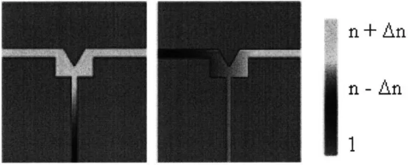
3.2.1 Localized Refractive Index Variation
On a local scale, the transmission and the splitting ratio of the high-transmission cavity (HTC) splitter are measured through simulation as a function of the amounts of localized refractive index variation due to possible temperature gradients within that part of the chip. Figure 3-2 depicts the simulation setup as two distinct stages. The splitter located on the left side shows a vertical effective refractive index variation gradient from n - An at the bottom of the splitting structure to n + An at the top of the structure. The splitter located on the right side of Figure 3-2 shows a horizontal effective refractive index gradient, also ranging from n -An to n + An.
I
~n+
An
n-An
Figure 3-2. Localized vertical and horizontal effective index variation for HTC splitter. (n=3.2).
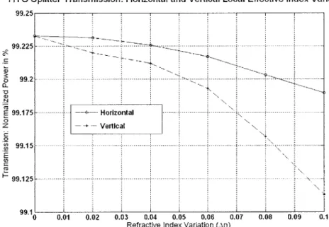
Figure 3-3 shows the results of transmission loss simulations for both the vertical and horizontal refractive index gradients. In the case of vertical refractive index variations, the transmission losses are examined as An ranges from 0 to 0.1, and there is a minimal loss of about 0.1% compared to the nominal transmission values. The same holds true for the total transmission losses with horizontal refractive index variation, as there is a drop of less than 0.1% with An = 0.1.
I - __ ! ___
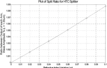
As far as the splitting ratio is concerned, there is a clear linear relationship between the amount of refractive index variation horizontally across the splitter structure and the optical power mismatch between the two output arms of the splitter. When exposed to a purely vertical refractive index gradient, however, there is no change in the uniformity of the split due to the symmetrical nature of the wave propagation direction as compared to the vertical gradient. Therefore, in Figure 3-4, the splitting ratio is plotted as a function of only horizontal refractive index variation (not vertical refractive index variation). The magnitudes of change in the splitting ratio are relatively small (0.9%) when compared to the change of 0.1 in the refractive index.
HTC Splitter Transmission: Horizontal and Vertical Local Effective Index Variation
99.25
99.175 -- Horizontal - --- - - --- - -
---Z - Vertical
99.1
0 0.01 0.02 0.03 0.04 0.05 0.06 0.07 0.08 0.09 0.1
Refractive Index Variation (An)
Figure 3-3. Transmission results for horizontal and vertical local effective index variation in the HTC splitter.
Plot of Split Ratio for HTC Splitter 1.W7B 0 0-05 1.004 E 1.003 ao) 1 CDr 0 >n 6 0.01 0.02 .03 0.04 0.05 0.06 0.07
efracdixe hdexVaiaton (An)
Figure 3-4. Splitting ratio results for the horizontal effective splitter.
0.08 0.09 0.1
index variation in the HTC
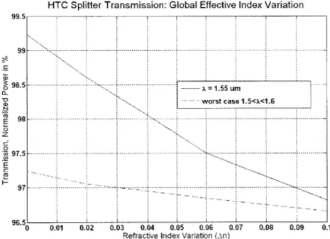
3.2.2 Global Refractive Index Variation
n
+ An
n
Figure 3-5. Global (chip-scale) effective index variation for HTC splitter. (n = 3.2).
At the global or chip-scale level, refractive index variation can occur to a higher degree than within a local space, and the impact of this variation can be substantial. Therefore, the analysis of chip-scale refractive index variation is critical in order to determine the robustness of the HTC splitter structure. Figure 3-5 shows the simulation setup for the global variation tests. Many different values for the refractive index of the
---material are used in order to simulate the different parts of the chip, whose localized temperatures may cause some deviations in the refractive indices. In each region, a uniform local temperature, and thus refractive index, is considered. Splitter to splitter mismatch on a global scale is now the concern, rather than the variation within the individual splitter.
Figure 3-6 shows a plot of the normalized transmission power versus the change in refractive index on a global scale. These results indicate that, for a change of An = 0.1 in the refractive index, a transmission loss of over 2% is realized. Furthermore, when considering the range of wavelengths from 1.5 ptm < X < 1.6 pm, the worst-case
transmission drops to almost 96.5%. Clearly, in order to design an efficient and robust optical signal distribution system, the chip-scale temperature distribution must be kept relatively uniform in order to minimize the refractive index variation seen by different splitters on the chip.
HTC Splitter Transmission: Global Effective Index Variation
99.5 9 8 .5 - ----- o~~ --- --- --- -- ---- I -------- ___ - 1.55 Urnu .... -worst case 1.5<X<1.6 E 98
.----~3
975 .--- ----97. 0 0.01 0.02 0.03 0.04 0.05 0.06 0.07 0.08 0.09 0.1Refractive Index Variation (An)
Figure 3-6. Transmission results for HTC splitter structure with global refractive index variations.
3.3 Geometric Variations
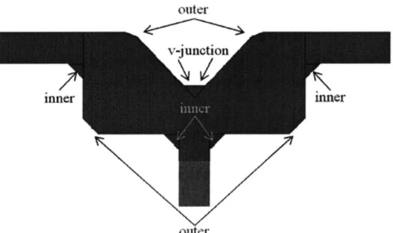
The geometric variations associated with a splitter structure can also have an impact on the characteristics of its performance. Geometric blurring along corners occurs during the lithography and etching processes, which then inhibits the robustness of the splitter. For example, in the high transmission cavity splitter shown in Figure 3-7, ten critical corners can experience geometric blurring due to lithographic processing. These ten areas are categorized into inner corners, outer corners, and v-junction corners as per their concavities. Here, the blurring is modeled as a triangular addition or subtraction from the original HTC splitter geometry. For the inner corners and v-junction, the blurring is modeled with the appending of a triangle to the existing structure at the blurring interface. For the outer corners, it is modeled by the truncation of a triangular segment from the original structure. The variation degree for the geometric blurring is represented by the length of a side of a triangular segment which has either been added or removed
from the original HTC splitter structure.
7 inner outer L-uncton inner outer
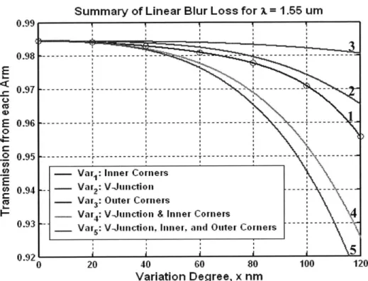
Simulations conducted by Staker reveal the impact of geometric blurring on the transmission of the HTC splitter [33]. Figure 3-8 plots the transmission from the output arms of the splitter as a function of variation degree. These results indicate that geometric blurring along the inner corners affect the performance of the splitter the most, while blurring along the outer corners is not as problematic. With a variation degree of 120 nm, the transmission loss reaches as much as 10%.
Summary of Linear Blur Loss for x = 1.55 um
E .
E
0 .-0.99 0.98 0.97 0.96 0.95i 0.94 0.93 0 20 40 60 80 100Variation Degree, x nm
Figure 3-8. Transmission results as a function of degree of geometric
various corners of HTC splitter.
120 blurring along
From these results, it can be concluded that waveguide splitter structures must be designed carefully to be robust to geometrical variation sources incurred during the lithographic process. In an on-chip optical signal distribution network, a signal may be propagated over long distances and pass through many splitter structures. In this case, the effect of blurring in one splitter is compounded many times as the optical signal
--- --- --- --- --- -- ----
---- Var: Inner Corners
- Var,: V-Junction
- Var: Outer Corners
- Var : V-Junction & Inner Corners
- Var: V-Junction. Inner, and Outer Corners
propagates from one point on the chip to another. Therefore, well-matched splitting ratios and well as low transmission losses are vital to the robustness of any optical signal distribution network.
3.4 Sidewall Roughness
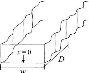
Sidewall roughness in waveguides, which is caused by uncertainties in the lithographic and fabrication process, can result in propagation losses over long distances. A simulation study was conducted to examine the impact of sidewall roughness on the
propagation losses of a straight dielectric slab waveguide. Figure 3-9 illustrates an example of sidewall roughness in a slab waveguide.
Figure 3-9. Sidewall roughness in a slab waveguide of width w and correlation length D, centered at x = 0.
The two parameters involved in this analysis are the standard deviation of the waveguide width, c, and the correlation length, D. The correlation length determines the relative distance across which the waveguide widths are correlated. For example, let R(d) denote an autocorrelation function of the width variance T2 from one point to another point d away. Then,
Id|
R(d) = a e (3-1)
Sidewall roughness can be separated into two variational components: width variation and position variation. Given a standard deviation a, two independent random variables can be constructed to model the sidewall roughness,
W ~ N(w, a2
) and X ~ N(O,(o/2)2)
(3-2) where W represents the waveguide width and X represents the coordinate of the center position of the waveguide. The standard deviation of the position is half that of the width so that the two variables are scaled properly and can be compared fairly.
Transmission Loss vs. Position and Roughness
0.14 0.12 ---- -- -- --- -- - --- - - - - --- --- --- ---0.8---____ 0 0.08 - - - - - -0- - . - - .- 0.0 F 3 p- Roughness Only
sdwl Roughness and Position
20.06
0.04-0.02 --- --- ---- ---- L - --- -- - -- -
-% ---- 0.002 0.004 0.006 0.008 0.01 0.012 0.014 0.016 0.018 0.02
cr (RMS Deviation) (ptm)
Figure 3-10. Impact of sidewall roughness on transmission power in a waveguide.
For a waveguide of width w = 0.2 ptm and a correlation length of 50 nm, the results of sidewall roughness analysis simulations are shown in Figure 3-10. The variation in the width of the waveguide, w, is denoted as the roughness variation. Similarly, the variations
in the center coordinate of the waveguide, x, is called position variation. The transmission loss through the waveguide increases as the standard deviations of the roughness and position increase, as is to be expected.
In addition, the results show that the sensitivity of the transmission loss to position variation is larger than its sensitivity to width variation. One possible explanation is that the confinement of the mode within the waveguide deteriorates quickly when the slab core itself shifts, but the confinement is still relatively good when the core region is stretched or shrunk, since the electromagnetic waves can still travel in a straight-line path. Work has been done in [5] to develop methods to reduce the sidewall roughness during the fabrication process as well as devise optimal waveguide dimensions to mitigate it.
3.5 Summary
This chapter discussed the effects of refractive index variation on the performance of the high transmission cavity splitter, which can be used as part of an on-chip optical signal distribution system. Results showed that the refractive index variation, resulting from temperature gradients across the chip, can have a significant effect on the optical power losses as well as the splitting ratios. The geometric blurring across corners due to lithographic uncertainties can also affect the transmission efficiency of the splitter structures. The design of an optical clock distribution network must include passive components which are variation tolerant because of their replication across a chip. Since effects of splitting ratios and transmission losses in a splitter are additive, each component must be robust to temperature gradients and geometric blurring. In addition, the impact of sidewall roughness on the propagation losses over long distances in a
waveguide was analyzed. Simulations revealed that the variation in the width of the waveguide, and to a greater extent, variation in the position of the waveguide, cause transmission losses.
Chapter 4
Optical Receiver Circuit Analysis
This chapter describes variation analysis performed on a short-pulse based optical receiver circuit for an on-chip clock distribution application. The first few sections provide an overview of the photodiode modeling and the receiver circuit under consideration. Then, the different sources of variation are described and analyzed in detail. These variation sources are optical input power variation, load capacitance variation, parasitic capacitive coupling, and static and dynamic noise. Finally the chapter is concluded with a summary of the results.
4.1 Overview
VDD
Figure 4-1. Ultrashort pulsed receiver circuit architecture [27].
The optical receiver circuit which will be the focus of variational analysis here is unlike that designed in previous implementations, in that the input is a fast-pulsed mode-locked optical input rather than a conventional continuous-wave laser [27]. The circuit architecture is shown in Figure 4-1. The reason behind the fast-pulsed lasing scheme is that it allows for low-jitter clock signaling due to the preciseness of the mode-locked
lasers. In addition, this simplified architecture, absent a transimpedance amplification
stage or extensive buffering stages, exhibits low capacitance and small area. The low
capacitance photodetectors and the minimal amount of circuitry allows for many of these
receiver circuits to be fabricated over the span of a chip.
The functionality of this ultrashort pulsed optical receiver circuit is the following.
Alternating short pulses are received at each photodiode, delayed by one-half the desired clock period. A pulse on the photodiode connected to the supply voltage will produce a
rising edge at the output, while a pulse on the photodiode connected to ground will
produce a falling edge at the output. After this clock signal is cleaned up by the static
CMOS inverter, a rail-to-rail square wave will be produced at the output, and a load can be driven using this clock signal.
At the optical-electrical interface, a number of specifications are required of both the
short pulses and the photodetectors. In order to supply sufficient power to generate a
clock signal that can drive an output capacitive load of 15 fF, the input optical power of each pulse must be approximately 430 piW. In addition, the requirements on the slew rate
of the clock and the preciseness of the clock edges require the duration of the input pulses
to be less than a picosecond (-100 fs). The wavelength of the optical signal is chosen to
be 850 nm, as that is the wavelength for which the quantum efficiency is the highest for
the photodiode.
The main characteristics required of the photodiodes are low capacitance and
relatively high responsivity. The responsivity is the ratio of photocurrent to input optical
R I
P,, (4-1)
P
To generate a robust gigahertz clock, the capacitance of the photodetectors are to be around 10-15 fF, while exhibiting a responsivity of about 0.5 A/W. Further details of the photodiode are discussed next.
4.2 Photodiode Details
A photodiode is a type of photodetector, traditionally operated in reverse bias with a
large biasing voltage, which generates electron-hole pairs caused by incident photons [23]. For this work in particular, the type of photodiode used is a p-i-n photodiode, which can be designed specifically to optimize certain parameters such as quantum efficiency by appropriately modifying the depletion thickness. The photodiode model used to conduct simulations is depicted in Figure 4-2.
Rs
p s) sC R RL It + Ri
T
..
.
Figure 4-2. Equivalent circuit model of a photodiode [23].
I, is the photocurrent generated as a result of the input optical power. Rj and C are the
junction resistance and capacitance, respectively. Both are governed by the dimensions of the depletion layer. R, is the series resistance, and I, represents a randomly varying current generated by the shot noise, while I, captures the thermal noise of the photodiode. Finally, RL and Ri are the external load resistance and the input resistance of an amplifier which may follow the photodiode, respectively.
Table 4-1. Sources of Variation in Ultrashort Pulsed Receiver Circuit.
# Type of Variation Detailed Description
1 Optical input power Caused by uneven power splits in the passive
variation waveguiding phase
2 Load capacitance variation Different loads across the chip will demand different drive strengths of the clock
Parasitic capacitive coupling Capacitive coupling with a nearby transitioning node can affect the output voltage
Static and dynamic power Static and dynamic power supply noise can affect 4 supply noise the output voltage by inducing skew, jitter, and
transition time variations
4.3 Critical Areas to Examine
The following areas, shown in Figure 4-3, are critical to the robustness of the circuit architecture, and therefore warrant detailed analysis. Table 4-1 describes each source of variation depicted in Figure 4-3.
4aND
3
'Vm
Figure 4-3. Sources of variation in ultrashort pulsed optical receiver circuit.
4.3.1 Optical Input Power Variations
As demonstrated in the previous chapters, accumulated transmission losses and uneven splitting ratios can be caused by geometric blurring in the waveguide splitter structures and refractive index variations. Thus, this variation will result in optical input power variations in the pulse trains at different parts of the chip. In addition, such
variations may also result in an optical input power mismatch between a single pair of photodiodes. The robustness of the circuit architecture against these variations and mismatches will be examined.
4.3.2 Load Capacitance Variations
Because the input power required by the circuit is directly proportional to the capacitive load it must drive, Cload must be the same everywhere across the chip for the receiver circuits to all function in the same way. However, load capacitances vary across the chip because of the way the designer chooses the placement and routing of the cells and wires. The amount of variation which the circuit will properly tolerate is important in determining the robustness of this ultrashort pulsed receiver circuit scheme.
4.3.3 Capacitive Coupling and Other Noise-driven Parasitics
Because of the dynamic nature of the node joined by the pair of photodiodes and the static CMOS inverter, parasitic capacitive coupling can have a detrimental effect on the performance of the receiver circuit. In addition, other noise-driven factors such as static power supply variation and dynamic power supply noise can impact the quality of the output signal. Particularly for clock signal propagation applications, it is important that the output waveform have sharp edges with high slew rates, rail-to-rail swing, and low skew and jitter. Therefore, it becomes necessary to examine the effects of parasitic capacitive coupling and environmental noise on this receiver circuit performance in order to determine its robustness.
4.4 Simulation Setup Parameters
The simulations conducted to determine the impact of variation on the optical receiver circuit are designed using a BSIM 3v3 0.18 pm model with a 1.8 V power
![Figure 1-1. Power-delay characteristics for optical and electrical interconnects [1].](https://thumb-eu.123doks.com/thumbv2/123doknet/13983113.454427/13.918.216.669.188.529/figure-power-delay-characteristics-optical-electrical-interconnects.webp)
![Figure 2-4. High transmission cavity [16] (left), Constant bending radius [5] (middle), Star- Star-coupler [17] (right).](https://thumb-eu.123doks.com/thumbv2/123doknet/13983113.454427/23.918.144.746.133.333/figure-transmission-cavity-constant-bending-radius-middle-coupler.webp)
![Figure 2-7. Diagram of clock skew and jitter in a clock distribution network [8].](https://thumb-eu.123doks.com/thumbv2/123doknet/13983113.454427/28.918.174.733.399.687/figure-diagram-clock-skew-jitter-clock-distribution-network.webp)