CRYSTALLIZATION IN SELF-IMPLANTED
POLYCRYSTALLINE SILICON-ON-INSULATOR
FILMS
byRalph Benhart Iverson
Bachelor of Science
Electrical Engineering and Computer Science Massachusetts Institute of Technology
(1979)
Master of Science
Electrical Engineering and Computer Science Massachusetts Institute of Technology
(1981)
Submitted to the
Department of Electrical Engineering and Computer Science In Partial Fulfillment of the Requirements
For the Degree of
DOCTOR OF PHILOSOPHY
at the
MASSA CHUSETTS INSTITUTE OF TECBNOL OG Y June, 1987
) Massachusetts Institute of Technology, 1987
Signature of Author
Department of Electrical Engineering and Computer Science
May 14, 1987
Certified by
Certified b -
L
IL. Rafael Reifihes
or
Accepted by
CRYSTALLIZATION IN SELF-IMPLANTED
POLYCRYS TALLINE SILICON-ON-INSULATOR FILMS
by
Ralph B. Iverson
Submitted to the Department of Electrical Engineering and Computer Science on May 14, 1987 in partial fulfillment of the requirements for the Degree of Doctor of Philosophy
in Electrical Engineering and Computer Science
Abstract
This thesis investigates crystallization in polycrystalline silicon-on-insulator (SOI) films amorphized by the implantation of silicon. Polycrystalline silicon films are deposited onto an oxidized silicon wafer by low-pressure
chemical-vapor deposition, implanted with silicon ions, and annealed. The crystalline fraction and grain density are measured by transmission electron microscopy as a function of implant dose, anneal time, and anneal temper-ature. These measurements are analyzed to determine the crystallization parameters of implanted polycrystalline SOI.
At low implant doses, the films are nearly amorphous; but enough crys-talline material is left that the subsequent anneal reproduces the morphol-ogy of the as-deposited films. As the dose is increased, fewer grains sur-vive; and the grains in implanted and annealed films are larger than in the as-deposited films. At still higher doses (the "channeling regime"), only grains which exhibit ion channeling survive; and the annealed films have larger grains and are textured as well. At large doses (complete amorphiza-tion) the final grain size saturates at 1-2 jum. The crystallization behavior at complete amorphization indicates that the final grain size is dictated by steady-state nucleation and growth rates after a transient time. The transient period is the time necessary to produce a steady-state cluster (microcrystal) population, which is a prerequisite to steady-state nucle-ation. The nucleation rate for doses between the channeling regime and complete amorphization is a strong function of implant dose. This is at-tributed to a population of clusters which is eradicated as the implantation dose is increased. This population is extinct at complete amorphization.
Thesis Supervisor: Dr. L. Rafael Reif
Acknowledgements
My foremost thanks go to my thesis committee, whose guidance has been instrumental in completing this work: my thesis advisor Professor Rafael Reif; and my thesis readers, Professors Dimitri A. Antoniadis and Henry I. Smith. I would also like to extend my thanks to several other deserving indi-viduals: Harry Atwater and Prof. Carl V. Thompson for information about crystallization processes; Mark Rodder for information concerning TFT's; Mike Frongillo and Gabriella Chapman for help with TEM; Tri-Rung Yew for c oss-sectional TEM work; Carolyn Zaccaria for administrative services; and numerous friends, whom I have burdened at times with thesis woes. I would also like to acknowledge the Mandala Folk Dance Ensemble for the regular relief from academia that it has provided me.
1 thank my parents, Ben and Ida, for their support. Finally, for the support she has always given me whether I needed it or not, I would like to express my gratitude to my wife Pat; though, I am more grateful than words can say.
This work was supported by the National Science Foundation (Grant No. 83-03450ECS) and the MIT Center for Materials Science and Engineer-ing (NSF-MRL Grant No. DMR84-18718).
Contents
Abstract 2 Acknowledgements 3List of Figures
6
List of Symbols
8
1 Introduction 102 Theory of Implantation Damage and Subsequent
Crystal-lization
16
2.1 Introduction ... 16
2.2 Implantation Damage in Polycrystalline Material ... 18
2.3 Crystallization ... 27 2.4 Conclusions ... 38 3 Experimental Method 42 3.1 Film Growth ... 42 3.2 Implantation ... 43 3.3 Recrystallization ... 44
3.4 Preparation for Transmission Electron Microscopy ... 44
3.5 Measurement Methods ... .. 45
3.6 Morphology of the as-deposited film ... 51
4 Dose Dependence of Final Grain Size 52 4.1 Experiment and Results . . . 53
5 Temperature Dependence of Crystallization Parameters in
Amorphized Silicon Films 59
5.1 Experiment and Results ... 60
5.2 Summary and Discussion ... 73
6 Crystallization in a "Seeded" Amorphous Film 76 6.1 Experiment and Results ... 77
6.2 Summary and Discussion ... ... 83
7 Dose Dependence of Crystallization Parameters in
Amor-phized Silicon Films 84 7.1 Experiment and Results ... 857.2 Summary and Discussion ... 94
8 Conclusions 96 8.1 Summary . . . ... 96
8.2 Suggestions for future work ... 100
A Survival Probability of an Implanted Grain 105 A.1 Analysis in terms of undamaged-area distribution ... 106
A.2 Virtual undamaged-area fraction ... 107
A.3 Survival probability . ... 109
A.4 Range of validity ... 111
B Spontaneous Crystallization
112
B.1 Crystalline fraction . . . .... 112B.2 Density of grains ... 114
B.3 Final grain size ... 1... 115
C Seeded Crystallization 116
List of Figures
i.1 Dose-dependent model of final grain size ... 22
2.2 Channeling directions in silicon . . . 24
2.3 Theoretical crystallization behavior ... 36
3.1 Micrograph of as-deposited film ... 51
4.1 Micrographs of implanted samples before and after recrys-tallization at 700°C ... 54
4.2 Dose dependence of final grain size ... 55
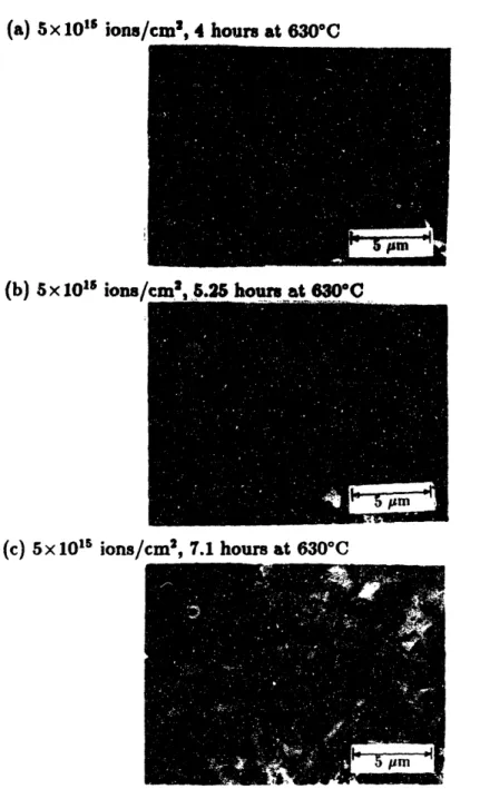
5.1 Micrographs of samples implanted at 5x101 5 ions/cm 2 and annealed for various times at 630°C ... 62
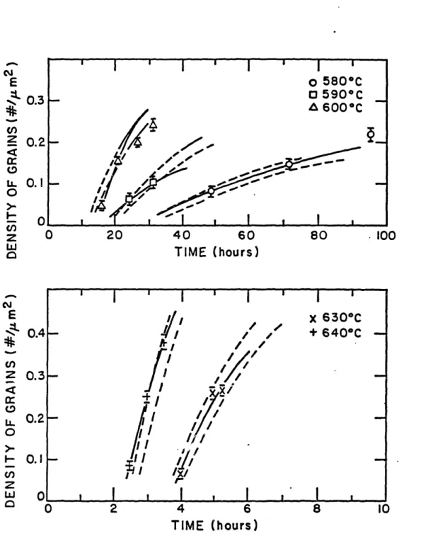
5.2 Density of grains versus anneal time and temperature after a dose of 5 x 10¹⁵ ions/cm 2 .
...
... 635.3 Crystalline fraction versus anneal time and temperature af-ter a dose of 5 x 10⁵ ions/cm2 ... 64
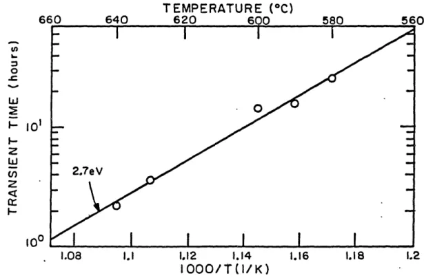
5.4 Transient time versus temperature ... 66
5.5 Nucleation rate versus temperature. ... 68
5.6 Characteristic spontaneous crystallization time versus tem-perature ... 69
5.7 Growth rate versus temperature ... 71
5.8 Final grain size versus anneal temperature ... 72
6.1 Micrographs of samples implanted at 2x10¹⁵ ions/cm2 and annealed for various times at 580°C ... 78
6.2 Density of grains versus anneal time after a dose of 2x10¹⁵ ions/cm2 ... 79
6.3 Crystalline fraction versus anneal time after a dose of 2 x 10¹⁵ ions/cm2 ... 80
6.4 Cross-sectional TEM micrographs of a partially
recrystal-lized film ... 82
7.1 Micrographs of samples implanted at 4x10: ions/cm2 and annealed for various times at 630°C ... 87
7.2 Density of grains versus anneal time after a doses of 4x 10¹⁵, 5x101 5, and 6x10¹⁵ ions/cm2 ... 88
7.3 Crystalline fraction after a doses of 4x1065, 5x101 5, and 6x10 5 ions/cm2. ... 89
7.4 Nucleation rate enhancement versus implant dose. ... 90
7.5 Time-evolution of cluster distribution. ... 93
List of Symbols
ca Amorphous fraction.
r(p) Gamma function,
fO
xP-le-Zdx.AG,, Free energy of formation of a cluster size n. A G Maximum free energy of formation of a cluster.
AGa_ Gibbs free energy difference between amorphous and crys-talline phases (energy/atom).
AGu,rf Interfacial energy (energy/surface atom).
e Film thickness.
v Jump frequency of an atom at a phase interface.
pg Density of grains (#/area).
Pn Density of nucleated grains (#/area).
ps Density of seed grains (#/area).
aOPg Standard deviation of measured grain density. aIx Standard deviation of measured crystalline fraction. r0 Transient time.
rn Characteristic crystallization time for nucleated crystalliza-tion (constant nucleacrystalliza-tion rate).
Tr Characteristic crystallization time for seeded crystallization. X Crystalline fraction.
Xn Crystalline fraction de to nucleated crystallization. Xs Crystalline fraction due to seeded crystallization.
AD Effective ion-damage area.
Ac Effective ion-damage area in oriented grains.
AG Grain area in annealed film.
AdaP Grain area in as-deposited film.
AG,n Final grain area due to steady-state nucleation.
AG,, Final grain area due to seeded crystallization.
Ed Activation energy of interstitial self-diffusion in silicon. Er, Activation energy of nucleation rate r,.
E,, Activation energy of transient time r0.
Er Activation energy of growth rate v.
fc Fraction of grains in a channeling orientation.
fd Dechannieling fraction of ions in oriented grains.
k* Reactioni rate at critical cluster size.
knn,+ Forward reaction rate of cluster size n.
k,+ln Reverse reaction rate of cluster size n + 1.
k Boltzman constant. n Cluster size.
n* Critical cluster size.
Nn Number of clusters of size n.
Pc Implant survival probability of a cluster.
PG Implant survival probability of a grain.
P~C Implant survival probability of an oriented grain.
PR Implant survival probability of a randomly-oriented grain. Q Implant dose (# ions/area).
Qc Channeling dose offset (# ions/area).
rn Steady-state nucleation rate (# grains/volume-time).
t Time.
T Absolute temperature.
Chapter 1
Introduction
This thesis investigates crystallization in polycrystalline silicon-on-insulator (SOI) films amorphized by the implantation of silicon. The crystalliza-tion process determines grain size which has a large effect on the electrical properties of the film and, consequently, on the characteristics of thin-film transistors (TFT's) well.
Silicon-on-insulator technology has become a subject of great interest and several techniques of film preparation have been investigated.l - 9 Some
techniques involve the melting of a deposited film: laser recrystallization of polycrystalline silicon;' lateral epitaxial growth from seeding windows by melting;2 and graphoepitaxy using a laser3 or strip-heater oven4 as a heat source. Other methods operate at lower temperatures, utilizing solid-phase processes: lateral solid-solid-phase epitaxy;5'6 seed selection through ion channeling (SSIC);7'8 and secondary grain growth.9
A layer of low-defect single-crystal SOI would expand the capabilities of VLSI enormously. Thin film transistors built in high-quality SOI would result in larger packing densities leading to larger memories, faster circuits,
and smaller chip sizes. The additional fabrication steps, however, increase the cost per wafer while decreasing yield.
The high processing temperature required by some SOI technologies cannot be combined with current VLSI processes because of the dopant diffusion and thermal stress it would cause. VLSI fabrication is more easily adapted to the lower-temperature SOI technologies which use solid-phase crystallization processes. In this regime, lateral solid-phase epitaxy prob-ably produces the highest-quality SOI. It does, however, require seed win-dows and therefore poses some restrictions on VLSI layout. Also, the lateral growth distance is only on the order of 5 /tm for undoped films.5 (A growth distance of 24 m was achieved6 with 3x10²° phosphorus atoms/cm s, but such material would be useful only as a conductor.)
Silicon-on-insulator applications other than VLSI are also attractive. SOI could be used to build devices and circuits on various substrates: on transparent substrates for flat-panel displays; on inexpensive substrates for solar-cells; and on different semiconductor materials for hybrid monolithic integration. Novel devices using SOI can also be envisioned.
Functional thin film transistors do not require a single-crystal layer of silicon, though the channel mobilities do correlate with the crystallinity. In fact, TFT's have been fabricated on amorphous as well as polycrystalline silicon films.1' - '2
Amorphous TFT technology has an advantage of lower processing tem-peratures than for polycrystalline silicon films. Channel mobilities of TFT's on amorphous silicon,l° unfortunately, are quite low: less than 1 cm2/V.sec for electrons.
In polycrystalline silicon films deposited by chemical-vapor deposition (CVD), the morphology is a function of film thickness. Thin films con-tain small grains. Thick films consist of a bottom layer of small grains with the remainder containing columnar grains. In all cases, the grain size is less than the film thickness. A 5000A layer of polycrystalline silicon deposited by low-pressure chemical-vapor deposition (LPCVD) has a grain size1 3 between 500A and 900k. The channel mobility in TFT's built on
poly-crystalline silicon is higher than for amorphous silicon, but lower than for single-crystal MOSFET's because of grain-boundary effects. One method of reducing grain-boundary effects is by hydrogen passivation.`4 Another is by reducing the number of grain boundaries (larger grain size). In small-grain polysilicon,ll the channel mobility is on the order of 10 cm2/Vsec for electrons.
Larger grain size can be produced by first amorphizing the polycrys-talline film by implantation and then recrystallizing it by a low-temperature anneal (550°C-700°C) .8 15'16In such a procedure, grain size of a few microns can be achieved. Recently, TFT's built on films prepared in this way12 had a channel mobility of more than 100 cm2/V.sec for electrons.
The goal of this thesis is to characterize the crystallization behavior of self-implanted polycrystalline silicon films, providing an understanding of how two major parameters (implant dose and anneal temperature) affect the texture and grain size in implanted and annealed films.
Ion implantation amorphizes a polycrystalline film according to the dose. As the dose is increased, more grains are amorphized. Certain crys-tal orientations (relative to the implant direction) are harder to amorphize
due to ion channeling 7- when the ion path is coincident with an axis or plane of high symmetry, the ion travels between the rows or planes of atoms and causes little damage. Because of the channeling effect, orientation ef-fects should be apparent over a range of doses (called the "dose-window") where "oriented" grains survive the implant and other (randomly-oriented) grains are amorphized. These oriented grains serve as seeds in a subsequent anneal. This process is called "seed selection through ion channeling", or SSIC.
The post-implant anneal crystallizes the film. Any grains that survive the implant will grow until they impinge upon one another. When there are no surviving grains, crystallization is from grains which nucleate spon-taneously.
Models of the amorphization and crystallization processes are derived in Chapter 2. Amorphization is a function of the implant dose. (The ion en-ergy and target temperature are also factors, but they are not varied in this thesis.) Classical nucleation theory (atomic scale) is presented. Crystalliza-tion in thin implanted films (microscopic scale) is then considered from two sources: from existing seed crystals (hereafter referred to as seeded crystal-lization); and from nucleated crystallites (hereafter referred as spontaneous or nucleated crystallization).
Chapter 3 explains the experimental methods common to the experi-ments presented here (Chapters 4-7): film growth; implantation; furnace anneal; preparation for transmission electron microscopy; and collection of data, including error estimation. Also, the morphology of the as-deposited film is described.
The experiments presented here (by chapter) are:
4. Dose Dependence of Final Grain Size in Amorphized and
Recrystallized Polycrystalline Silicon Films.
8This experiment
involves several samples of polycrystalline silicon. Each is implanted with silicon. The dose is varied from 1x10¹⁴ to 5x101 ions/cm2 in order to produce a different degree of amorphization in each sample. The samples are then completely recrystallized by a low-temperature anneal. The experimental results (final grain size as a function of implant dose) are compared with a model (from Chapter 2) which accounts for channeling effects. Also included and providing further evidence of the channeling effect are the results of related experiments by Kung et al.19-2 1 using X-ray pole-figure analysis to investigate the {110} texture of implanted and annealed films.5. Temperature Dependence of Crystallization Parameters in
Silicon Films Amorphized by Implantation. 2 3 In this experi-ment, several polycrystalline silicon films are implanted with 5x 10¹⁵ ions/cm2, enough to destroy virtually all seed crystallites. At each of five temperatures (580°C, 590°C, 600°C, 630°C, and 640°C), crystal-lization parameters are determined from the collected data (density of grains pg versus anneal time, and amorphous fraction X versus an-neal time). Activation energies are then determined, based on the calculated parameters at the five anneal temperatures. The activa-tion energies determine some of the thermodynamic parameters used in classical crystallization theory (Chapter 2).
6. Crystallization in a "Seeded" Amorphous Film.2 2 In this ex-periment, a polycrystalline silicon film is implanted with 2x10¹⁵ ions/cm2. This dose is selected to produce an amorphous film with approximately 25 grains/Im 2. The film is then annealed at 580°C for varying lengths of time. The density of crystallites and the crystalline fraction (as a function of anneal time) indicate that the source of crys-tallization is probably due to microcrystals, not due to seed grains as originally presumed. (Crystallization was originally thought to be due to seed grains since nucleation in amorphous silicon produces less than one grain per square micron.)
7. Dose Dependence of Crystallization Parameters in Silicon
Films Amorphized by Implantation.
24This final experiment
shows how the crystallization parameters vary with implant dose. Three doses are used: 4x10¹⁵, 5x10¹⁵, and 6x10¹⁵ ions/cm2. The parameters are determined at 630°C. T'hese results are combined with data from the previous experiments to provide a global picture of the effect of implant dose on crystallization.
Chapter 8 reviews the theoretical and experimental results of this work and includes several suggestions for future work.
Chapter 2
Theory of Implantation
Damage and Subsequent
Crystallization
2.1 Introduction
This chapter contains the theory which served as the original hypothesis of this work: the effect of implantation on the structure of polycrystalline silicon, the classical theory of nucleation and growth, and the crystallization behavior of films from seed grains and from nucleated grains.
The effects of implantation on crystallinity in single-crystal silicon have been investigated intensively25- 3 2 and are fairly well described. In this chapter, implantation effects are extended theoretically into the domain of polycrystalline films. The theory is presented here as it was hypothesized before any experimental confirmation. A modification indicated by sub-sequent data (Chapters 4-7) is outlined in the concluding section of this chapter.
theoreti-cal background necessary for understanding crystallization processes on an atomic scale, where implantation effects are manifested.
Crystallization is analyzed on a microscopic scale because data are col-lected on the microscopic scale. Density of grains p,(t) and crystalline fraction X(t) are the two quantities measured to determine the crystalliza-tion parameters. Crystallizacrystalliza-tion of polycrystalline films is assumed here to arise from two sources: the growth of seed grains; and/or the growth of grains nucleating at a steady-state rate. Given a constant growth velocity
v9 and either an initial density of seeds p, or a constant nucleation rate r,,
crystallization becomes a geometrical problem. This was first treated by Johnson and Mehl33 and by Avrami.3 4 3 6 One other crystallization param-eter, ro is also used - it is the initial transient time, during which little nucleation occurs. The measurements used in this thesis are: the crys-talline fraction x(t) and the density of grains p,(t) in partially annealed films; and final grain size Aa in 100% recrystallized films. These quantities are derived here in terms of the crystallization parameters (vg, rn, pa, and
To) which, in turn, are found in terms of some thermodynamic parameters
used in classical nucleation theory. In later chapters, the crystallization parameters vg, r, p,, and r0 are extracted from the crystallization data
(X(t), p(f), and AG) using the theory developed in this chapter. From v,,
rn, p,, and r0, thermodynamic parameters of the classical nucleation theory are found.
2.2 Implantation Damage in Polycrystalline
Material
In this section, the model of implantation damage in polycrystalline silicon is developed. Ion implantation damage is first described in a crystalline material. Then the basic model is developed. This theory treats the impact positions of the ions as random on an atomic scale, as opposed to uniform on a microscopic scale. Ion channeling is then described and its effects are included in the model.
2.2.1 Ion Implantation
When a high-energy ion enters a target, it loses energy through coulombic interactions with electrons and with target nuclei. Because electrons are much lighter than ions, each interaction is small. The cumulative effect, therefore, is to uniformly slow any incident ion. The trajectory can be greatly influenced, however, by interactions with target nuclei, depending on the relative masses. These interactions are usually analyzed to determine the implant profile (the position profile of the final ion positions).
The ion energy transferred through collisions with the nuclei is called "damage energy" since an ion-nucleus interaction can impart enough energy to a target nucleus to displace it. (In fact, the energy transferred can be high enough that the displaced nucleuls needs to be treated as a secondary energetic ion in detailed damage-energy calculations.3 7'3 8) In a crystalline material, implantation produces a degree of amorphization which depends on the implant dose. Since all energy lost is ultimately manifested as heat,
it is also possible for some self-annealing to occur. To minimize heating during an implant,. therefore, low implant current and/or reasonable heat-sinking is required.
To first order, the amorphization (lattice damage) caused by a beam of high-energy ions is proportional to the damage energy which, in turn, is proportional to the ion dose. This model has been used to calculate the amorphization dose as a function of energy. A critical damage energy for single-crystal silicon of 12 eV/atom has been determined by Narayan
et al.32 Assuming damage is uniform and the depth of the damage is known, the dose required to amorphize a layer of silicon can be easily found. The value of 12 eV/atom, it should be noted, is not the energy required to knock a silicon atom out of its lattice position. It is no more than the average damage energy per atom that needs to be deposited to ensure that no significant crystalline areas remain.
The assumption that the amorphization damage is proportional to dose is adequate in some cases. The paper by Narayan et al., however, also shows that the amorphous region contains microcrystallites. This is because on the atomic scale the ion trajectories are random (not uniform); some small volumes are less damaged than others. If an implanted layer is being regrown epitaxially, the microcrystallites (which are of the same orientation as the substrate) have little or no effect. In amorphized polycrystalline silicon on oxide, however, these microcrystallites are of major importance since they may serve as seeds in the absence of a seeding substrate.
In 1981, Komem and Hall1 5 reported a dose dependence of the final grain size in polycrystalline silicon films which were implanted with germanium
and annealed. They found that an annealed film which was implanted with a dose of 2 x 10¹⁵ ions/cm2 was similar to the deposited fim; however, as-annealed film which was implanted with a dose of 4 x 10¹⁶ ions/cm2 consisted of large (over 1 im) dendritic grains, about 10 times larger than in the as-deposited film. By transmission electron microscopy (TEM), the two as-implanted films were amorphous - there were no observable differences in crystallinity. The ability of the low-dose sample to recover its original morphology was attributed to "memory" of grain boundaries - it was suggested that at a sufficiently small dose, the grain boundaries survive and block crystallization. In this work, the memory effect is attributed to microcrystallites rather than to grain-boundary memory.
2.2.2 Survival Probability of Grains in Polycrystalline
Material
The implant dose controls the degree of amorphization of a polycrystalline film. On an atomic scale, the impact positions of the ions are random (not uniform). This means that at a given dose, grains may survive the
implant due to chance - either few ions may hit a grain or those that hit may be more concentrated than average, leaving some part or parts of the grain relatively undamaged. The model developed here assumes that upon implantation, each grain is in one of two states: a grain may be completely amorphized; or enough crystalline structure survives to serve as a seed in a subsequent anneal. The trace crystallinity in as-implanted films is too small to be measured by conventional methods like transmission electron microscopy (TEM) or Rutherford back-scattering (RBS). In Chapter 4, the
probability that a grain survives the implant, PG is found experimentally by recrystallizing the film at a low temperatures (7000C) and determining the average final grain size: AG = AdP/PG. This assumes that (1) there is no spontaneous nucleation and (2) each surviving grain results in only one seed (multiple crystalline regions within a single grain "unite" upon annealing). The first assumption is accounted for later in this chapter. The second, however, is maintained throughout this work in view of the ability of epitaxial regrowth to reclaim microcrystals in the amorphized layer of single-crystal silicon, as noted above.
In addition to treating the impact positions as random rather than uni-form, the volume of damage associated with each ion is modeled as an effective area AD which depends on the implant parameters (ion energy, ion-target combination, and target temperature). This is an effective area because crystal structure may survive at any depth. Moreover, this is an
average effective area because the cascades (paths of primary and secondary
ions) due to identical ions may vary significantly. At high energies, a pri-mary ion displaces target nuclei at large irregular intervals. At low energies, the damage is more dense.
The probability of a grain surviving an implant is analogous to the probability that a tile in a room is not completely covered when one tosses in a large number of coins. In this analogy, the tile represents a grain of polycrystalline silicon and each coin represents the damage caused by a single ion. This problem has two parameters (AdeP and AD) and one variable, the dose Q (represented in the analogy by the number of coins per unit area) and is solved in Appendix A. The solution is written here as
z
I
Wr
L 3 w 10 Uz
:Cz
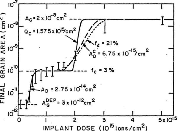
Z 10 N Z lo Ct) z 0 500 1000 1500 NORMALIZED DOSEFigure 2.1: Normalized final grain size versus normalized implant dose for several values of normalized damage area AD based on Eqn. (2.1). All quantities are normalized to the initial grain size AGP
- In (1 - PR) = 2Q2AdPAD exp (-QAD) (2.1)
and is valid for QAD > 4.6. The superscript on PG denotes that this is the survival probability in the absence of channeling - as described further on, damage in grains which exhibit channeling effects is modeled by modifica-tions to Eqn. (2.1). Figure 2.1 shows a theoretical plot of the normalized final grain size versus normalized implant dose with all areas normalized to
2.2.3 Ion Channeling
Implantation damage is a function of dose, ion species, and implant energy. In crystals, it is also a function of the implant angle. When the path of the ion is nearly parallel to a high-symmetry axis of the crystal, the ion usually channels (passes between rows of atoms); as the ion nears any row of atoms, the cumulative interaction with the row deflects it away even though the interaction with each nucleus in the row is small. Little damage occurs in this case and the trajectory of the ion is straight and much longer than in a random (non-channeling) direction.3 9- 4' The orientation-sensitivity of
amorphization was shown dramatically by Nelson and Mazey17 who
im-planted
{100},
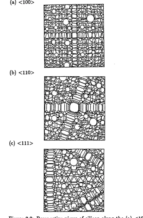
110}, and {111} silicon wafers from a point source at close proximity. Each position on a wafer, therefore, corresponded to implanta-tion in a particular crystallographic direcimplanta-tion. The degree of amorphiza-tion in these wafers could be qualitatively determined optically. All major planes and axes exhibited less amorphization than other (random) direc-tions. Other research of channeling damage has also been done,44- 46 but none demonstrate the effect in such a visual form. The major channeling direction is <110>, as is suggested in Fig. 2.2, which shows perspective views of silicon along <100>, <110>, and <111> channels.2.2.4 Channeling Effects in Polycrystalline Silicon
Channeling also occurs in polycrystalline silicon, but only in properly ori-ented grains. Channeling through polycrystalline silicon was reported in 1979 by Seidel.47 When implantation was used to phosphorus-dope the
(a) <100>
(b) <110>
(c) <111>
Figure 2.2: Perspective views of silicon along the (a) <100>, (b) <110>, and (c) <111> channels.
polycrystalline silicon gate of an NMOS enhancement-mode transistor, it became a depletion-mode device, even though the implant depth was less than the gate thickness. This effect was eliminated by any of three meth-ods: amorphization of the top of the gate material; thermal oxidation of the top of the gate material; or reduction of the implant energy.
A novel low-temperature SOI process, proposed in 1981 by Reif and Knott,48 utilizes the orientation-dependence of implant damage to selec-tively amorphize polycrystalline silicon:
1. Deposit polycrystalline silicon on a thermally oxidized wafer. How-ever, any non-seeding substrate able to withstand 625°C (deposition temperature of the silicon film) is suitable.
2. Implant with enough silicon ions to amorphize the film only where no channeling occurs. By implanting from appropriate angles, only grains of one orientation should survive. Hereafter, these grains are called "oriented grains", meaning that they are oriented with respect to the ion beam such that the ions channel. Other grains are called "randomly-oriented grains". This step is called "seed selection by ion channeling", or SSIC.
3. Anneal at a low temperature to crystallize using the surviving grains to seed the film.
The implant dose must fall within a range of values called the "dose win-dow": if the dose is too small, grains of random orientations survive the implant; or if the dose is too large, all the grains are amorphized.
a function of implant dose - within the dose window, the final grain size should be larger than the as-deposited grain size, and yet it should be only a weak function of dose. Equation (2.1) can be modified to include grains which exhibit channeling. The forms used here assume that a fraction f of the as-deposited grains exhibit channeling effects and that the same degree of channeling occurs in each of these grains. This is a simplification of what is actually expected because different orientations support different degrees of channeling.
Three models are considered here for the survival probability, Pg, of an oriented grain:
1. Assume implantation damage is negligible below a critical ion dose
Qc (so that PG = 1) and that above Qc the damage is the same as for
randomly-oriented grains. For oriented grains, survival probability is found at doses above Qc by substituting (Q-Qc) in place of Q in Eqn. (2.1):
- In (1 - PC) = 2(Q - QC)2
A
' AD exp [-(Q - Qc)AD)] (2.2)2. Assume that implantation damage is due to a dechanneling fraction
fd of ions. The survival probability is found by substituting fdQ in
place of Q in Eqn. (2.1):
-In (1 - PC) = 2fd2Q2 A 'PAD exp (-fdQAD) (2.3) 3. Assume that the volume and magnitude of ion damage in oriented
In this case, the survival probability is found by using a smaller ef-fective damage area AO in place of AD in Eqn. (2.1):
- n (1 - PGC) - 2Q2A PA exp (-QAD) (2.4)
2.2.5 Density of seeds
The density of seeds p, in an implanted polycrystalline silicon film is the sum of the density of randomly-oriented surviving grains and oriented sur-viving grains:
Ps = [(1 - fc)P + (fc)P]
A,
(2.5)
where f, is the fraction of grains that exhibit channeling effects. The survival probability of a randomly-oriented grain, pR, is calculated by Eqn. (2.1). The survival probability of an oriented grain, Pc, is calculated by one of three modifications to Eqn. (2.1): Eqn. (2.2), (2.3), or (2.4).
In the absence of nucleation, the grain size upon crystallization is AG,, =
1/p,. From the theory presented so far, two plateaus should be observable
in a plot of final grain size AG versus implant dose Q: at low doses, few grains (oriented or randomly-oriented) are amorphized completely so that
AG .ACp ; and within the dose window, most randomly-oriented grains are
completely amorphized though few oriented grains are so that AG ~ Ad/f, p .
2.3 Crystallization
Nucleation during crystallization affects the grain size and texture of the annealed film. Since nucleation increases the density of crystallites, the final
grain size is smaller than indicated by Eqn. (2.5). Furthermore, nucleated grains are not expected to conform to the orientation selectivity of ion channeling within the dose window. The following sections describe the classical theory of nucleation and growth, crystallization due to a steady-state nucleation rate, crystallization from seed grains, and crystallization from a combination of seed grains and nucleated grains. The nomenclature used here is loosely based on the nomenclature in a paper by Kelton et al.49 on transient nucleation.
2.3.1 Parameters of nucleation theory and
crystalliza-tion behavior
The parameters used here can be divided into two sets: parameters which are used with thermodynamics to describe crystallization on an atomic level; and the crystallization parameters which are more directly measured, such as growth velocity, nucleation rate, and characteristic crystallization time.
The three energies used here to describe crystallization on an atomic
level are:
* The difference (per atom) in Gibb's free energy between the amor-phous and crystalline phases (AGa-_);
* The energy required (per interface atom) to maintain an interface between the two phases (AG,,,f); and
* The activation energy Ed associated with the unbiased jump fre-quency v of an atom at the interface. (The unbiased frefre-quency is
the frequency at which an interfacial atom would change phases given that there is no net change in energy.)
As shown in this chapter, these three energies are related to the temperature-dependence of the "microscopic-scale" parameters of crystal-lization:
* A growth velocity v, which is assumed to be time-independent; * An initial transient period r0, during which no nucleation occurs; and,
* A steady-state nucleation rate r starting at time t = r0.
(There are also characteristic times of crystallization for growth from seed grains, r,, or from nucleated grains, rn, but these can be described as func-tions of v,, r, and the initial seed density p,.)
2.3.2 Classical theory of nucleation and growth
The classical theory of nucleation and growth postulates the existence of crystalline clusters so small that they are unstable, tending to shrink be-cause the energy required to maintain the crystalline-amorphous interface outweighs the Gibb's free-energy difference between the crystalline and amorphous phases.
Consider an amorphous medium with no clusters. With time, the sys-tem tries to reach thermodynamic equilibrium, for which the relative pop-ulations (by cluster size n) of clusters can be easily determined from the total free energy of formation (interfacial energy - phase energy
squared) and the energy difference between the phases is proportional to the volume (radius cubed). clusters larger than a critical size n' grow to mini-mize the free-energy of the system. In other words, the system cannot reach a thermodynamic equilibrium cluster population in an amorphous medium
- the "super-critical" clusters grow until the system is crystalline. The system can, however, approach steady-state within the amorphous fraction, in which one can observe a steady-state nucleation rate (per amorphous volume), even though the amorphous fraction decreases with time.
According to classical theory, microcrystallites (containing only a few atoms) nucleate frequently. Because of a large surface-to-volume ratio these tend to shrink. From thermodynamic considerations, however, a few be-come large enough that further growth is energetically favorable. Growth in the microcrystalline regime occurs by the same basic mechanism as growth in the "macrocrystalline" regime: the rate at which each atom at an amorphous-crystalline interface makes a transition between the amorphous state and the crystalline state is a function of the energy levels of the two states. Growth is energetically favorable when the free energy of the system is lowered by the transition of an interface atom from the amorphous to the crystalline states.
The free energy of formation AG,, of a cluster of size n consists of two components: the Gibbs free energy difference between crystalline and amor-phous phases (proportional to volume, or n); and the energy required to maintain the amorphous-crystalline interface atom (proportional to surface area, or n2/3). The Gibbs free energy difference between the amorphous and crystalline phases is denoted here as AG_,- and is in units of eV/atom. It is
taken to be positive. That is, the energy of each atom in the cluster is lower than the energy of an atom in the amorphous phase by AGa_,. The inter-facial energy is denoted here as AG,,,, and is in units of eV/surface atom.
The free energy of formation of a cluster size n may be written
AG = Cn2/3AGjurf - nAGa-, (2.6)
where C is a geometrical parameter related o the the shape of the cluster. At small cluster sizes, the interfacial energy outweighs the energy differ-ence due to the phase change - the net free energy of formation AG, is positive. The maximum free energy of formation, denoted AG*, can be found from Eqn. (2.6) and occurs at what is called the critical cluster size, n'. This energy enters into the temperature dependence of the steady-state nucleation rate rn.
The forward reaction rate k,_n,+l is the rate that a cluster grows from n to n+l atoms. The reverse reaction rate k,+l,, is the rate that a cluster shrinks from n+l to n atoms. These rates are found by defining an unbiased atomic jump frequency v at the amorphous-crystalline interface. Since is probably closely related to the jump rate in the amorphous phase, it can be characterized by the activation energy, Ed, of self-diffusion in amorphous silicon:
v c exp (-Ed/kT). (2.7)
Since all reaction rates are proportional to v, Ed enters into the activation energies for transient time r0, steady-state nucleation rate r, and growth velocity vg.
The reaction rates are also proportional to the number of atoms at the cluster surface and may be written in the following form:
k,.,+l oc n2/3 exp (-Ed/kT) exp [(AG,,+ - AGn)/2kT], and
knl,, oc n2/3exp(-Ed/kT)exp[(AG, - AG,+l)/2kT]. (2.8)
A complete analysis of the reaction rates (Eqn. (2.8)) and AG, (Eqn. (2.6)) provides values for the crystallization parameters transient time, nucleation rate, and growth velocity within the scope of classi-cal theory. The activation energies of the crystallization parameters, as shown below, are related to AG', AGa-, and Ed. The transient time is the effective time to reach a steady-state nucleation rate from the initial conditions (no clusters). At steady-state, the number of clusters N, of each cluster size n is time-independent and the net forward reaction rate
(Nnkn-n+l - Nn+lkn,,+l-,) is equal to the steady-state nucleation rate r,
for all n. Growth velocity is found from the net forward reaction rate for a large cluster.
2.3.3 Transient nucleation time
A number of analyses of transient nucleation have been published. 5 - 4 In each case, a characteristic time rt associated with transient nucleation was found to have the same temperature dependence. Assuming that the free energy of formation is a weak function of temperature, the form is
rt T/k, (2.9)
where k* is the forward (or reverse) reaction rate at the critical cluster size. From Eqn. (2.8),
k* oc n'2/3 exp (-Ed/kT).
Kashchiev's theoretical results,64 which are in good agreement with ex-periment, indicate that the transient time r0 is proportional to rt, so that
ro c Texp (Ed/kT). (2.11)
The linear temperature term in Eqn. (2.11) contributes kT to Ero (defined here as the slope of ro on an Arrhenius plot):
d Idn(ro)
d(1/kT)
Ed - kT.
(2.12)
Since Eqn. (2.11) does not have a true Arrhenius form, Eo in Eqn. (2.12) is not a true activation energy. For the anneal temperatures used in this thesis, however, kT varies only slightly around 0.075 eV. The Arrhenius form is taken here to be exp (E/kT) for times (0 and
n,)
and exp (-E/kT) for rates (r, and v)2.3.4 Nucleation rate
The theoretical temperature dependence of the steady-state nucleation
rate49 is 1
r aoc exp [-(Ed + AG.)IkT]. (2.13) The product of Eqns. (2.11) and (2.13) is:
Torn = exp (-AG IkT) (2.14)
and the maximum free energy of formation of a cluster can be written as
AG
=
Er -E,
(2.15)where EIn is the absolute slope of r, on an Arrhenius plot.
2.3.5 Growth rate
The growth rate can be found from the net forward reaction rate for a large cluster. Addition of one atom to a large cluster does not significantly change the surface energy. The change in free energy, then, is -AG_-. From Eqn. (2.8), assuming AG.-_ > 2kT,
dn
d- -kn-- n.+l -knoln
dt
oc n2/ 3exp (-Ed/kT) x
[exp (AG_,.I2kT) - exp (-AG_,I2kT)
oc n2/ 3exp[-(Ed - AG_./2)/kT]. (2.16)
Because n is proportional to the radius cubed (r3), Eqn. (2.16) is easily solved for v, (= dr/dt):
Vg,
c exp [-(Ed -
Ga-_.2)/kT]
.
(2.17)
The Gibbs free energy difference between the amorphous and crystalline phases, therefore, is:
AGa_, = 2(E,, - Ed), (2.18)
where E,, is the activation energy of the growth velocity.
2.3.6 Crystallization due to nucleation
Crystallization due to nucleation of grains is analyzed in Appendix B using steady-state nucleation and growth rates. Whereas the nucleation rate is initially zero (assuming no clusters initially) and rises during a transient
period towards a steady-state value, we assume here that this can be rea-sonably modeled by no nucleation during an effective transient time r0 and
a steady-state nucleation rate r, thereafter. This can be represented by a shift of the time axis: t - t-r0.
From Eqn. (B.6) the crystalline fraction in a film of thickness as a function of anneal time becomes
X(t) = 1 - exp {-[(t- ro)/rs} (2.19)
where T, is the characteristic crystallization time due to nucleation and is
given by
= 1/ ' V,2Er (2.20)
The density of grains (from Eqn. (B.10)) is still
pn(t) = ernrn g(u), (2.21)
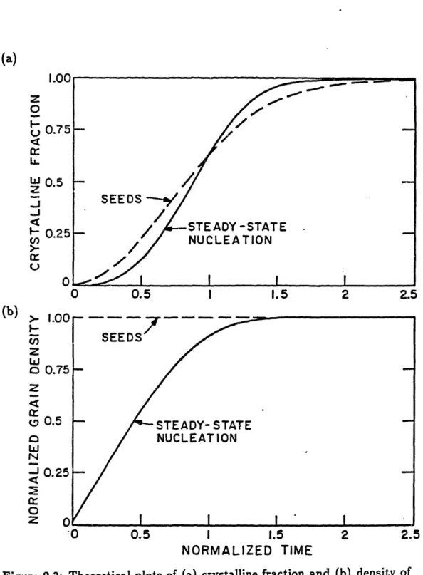
but the normalized time parameter u is now redefined as (t - ro)/r,. The function g(u) is defined in Eqn. (B.9). For t << r,, g(u) u and the density of grains is linear in time: p,(t) = Ern(t-ro). For t > r, g approaches r (4). The solid lines in Figure 2.3 are theoretical curves of the crystalline fraction and the density of grains versus normalized anneal time assuming a constant nucleation rate. The density of grains is normalized to the final density.
2.3.7 Crystallization from seed grains
Crystalline fraction is determined in Appendix C as a function of anneal time for crystallization from an initial seed density p, assuming no nucle-ation:
(a) . \ , I .Uu Z
0
u 0.75
Cr i.. w 0.5z
JJ
[" 0.25 (,/ >.. U 0 0 0.5 1 1.5 2 2. 112 I ') ,_z
-CnZ
W0
OZ0
W w N I cc0
2 '0 0.5 1 1.5 2 2. NORMALIZED TIMEFigure 2.3: Theoretical plots of (a) crystalline fraction and (b) density of grains (normalized to final density) versus normalized time. The solid lines are for crystallization due to a constant nucleation rate. The dashed lines are for crystallization due to seed grains.
5
(2.22)
X = 1 -
exp
[-(t/r.)2],where r, is the characteristic time of crystallization in a seeded film:
, = 1/ 2p,. (2.23)
The dashed lines in Figure 2.3 are theoretical curves of the crystalline fraction and the density of grains versus anneal time (normalized to r,) assuming crystallization from seed grains.
2.3.8 Competition between seeded and spontaneous
crystallization
In implanted polycrystalline silicon films, seed grains which survive im-plantation may compete with grains that nucleate spontaneously. The crystalline areas resulting from these two sources may be considered in-dependent, as is done in Appendices B and C The crystalline fraction as a function of time, then, is
1 - exp It/,] 2 t <TO (2.24)
X(t)
=1
-exp
(-[(t- o)/n]3 -[t/] 2} t > o (2.24)where r, and r, are defined in Eqns. (2.20) and (2.23) respectively. The density of grains versus time is given by
Ps(t) = p + .er. [1 - x(t')] dt'. (2.25)
Because of the complicated form of X in Eqn. (2.24), this can only be solved numerically (by computer) or approximately (by a Taylor series expansion of the integrand, for example).
The final grain size is smaller than 1/p, because any nucleation increases the density of grains. Also, the final grain size is larger than 1/[p, + p,(oo)]
since fewer grains nucleate than in an unseeded film because the amorphous fraction within which nucleation occurs is smaller. (p,(t) is the density of grains assuming no initial seeds exist.)
2.4 Conclusions
The theory developed in this section predicts the crystallization behavior of implanted polycrystalline films and is embodied by Eqns. (2.24) and (2.25) and associated equations - crystalline fraction X and density of grains pg are the two quantities determined experimentally as functions of implant dose, anneal temperature, and anneal time and from which parameters of the crystallization model are extracted.
The dose dependence is found in the parameter p, (in Eqn. (2.25)) as determined by Eqns. (2.1) through (2.5). The temperature dependence is found in the crystallization parameters r0, r,, and v. in Eqns. (2.11), (2.13)
and (2.17). The time dependence is found in X and p, in Eqns. (2.24) and (2.25).
This theory predicts three plateaus in the plot of final grain size versus implant dose:
1. At low doses, the small degree of amorphization has little bearing on the morphology of the annealed film. Enough crystalline structure of each grain is retained to serve as a seed. The final grain size, therefore, should be approximately the same as before the implant and the texture should be unchanged.
en-tirely. Neighboring grains which survive the implant grow into the space formerly occupied by these grains. The resulting average grain size is therefore assumed to depend only on implant dose. Channel-ing effects should result in a "dose window", where most grains are amorphized and those that survive the implant do so because they are oriented with a major crystallographic direction parallel to the ion beam. Within this window, the final grain size should not be a strong function of implant dose and the annealed film should contain only grains that exhibit channeling effects.
3. At large doses, so few grains (oriented or otherwise) survive the im-plant that crystallization proceeds by the growth of homogeneously nucleated grains. Because nucleation and growth rates are strong functions of temperature, the grain size in this regime depends on anneal temperature but not on dose.
From this theory, orientation effects should be apparent in the second plateau only - the first plateau contains randomly-oriented grains from the as-deposited film and the third plateau contains nucleated grains.
The experimental results of this work support the theory as presented but requires a basic refinement: the microcrystals which survive implanta-tion above 2x 10¹⁵ ions/cm2 are small enough that they must be regarded as sub-critical clusters. This resllts not in seeded crystallization, but in crystallization due to a large nucleation rate. (This does not necessarily preclude seed selection by ion channeling, since the clusters may retain the orientation of the as-deposited grain.)
The as-implanted cluster population is a strong function of implant dose and is also a function of cluster size. In Appendix A, an intermediate func-tion PA is defined as the distribution by size of the undamaged regions. This function includes the as-implanted cluster population. However, since PA is not explicitly determined, a first-order model is proposed here. Consider a cluster with cross-sectional area Ac and thickness se. For a single ion hit, assume that the probability of annihilation is proportional to e, since at large implant energies the distance between ion-nuclei interactions can be large. The "annihilation dose", then, is Q' = CQ~E, where C is a constant. The survival probability is given by
Pc = exp(-Q'Ac)
= exp (-CQAcE,)
= exp (-C'Qn),
(2.26)
where C' is a constant. A more exact formulation would consider that the clusters do not exist initially, but are a result of amorphizing most of a crystalline material. This could be represented by a dose offset, which would probably be a function of cluster size. The major point raised by Eqn. (2.26) is that the number of clusters of size n should decrease expo-nentially with implant dose and, furthermore, large clusters are amorphized faster than small clusters. From Eqns. (2.26) and (B.11), the final grain size increases exponentially with dose if the nucleation rate can be considered proportional to the number of clusters.
For the films used here, at doses below approximately 5 x 10¹⁵ ions/cm2,
a steady-state distribution is achieved. Above 5 x 10¹⁶ ions/cm2, the initial cluster population is so small that no nucleation occurs during the tran-sient time. Around 5x10¹⁶ ions/cm 2, few enough clusters exist that the nucleation rate is low during the transient period and the final grain size is actually larger than can be achieved at higher or lower doses.
Chapter 3
Experimental Method
This chapter describes how the polycrystalline silicon films are grown, implanted, annealed, and prepared for transmission electron microscopy (TEM). The last sections describe TEM and how the data is extracted from the micrographs.
3.1 Film Growth
Two-inch [100] lightly-doped n or p-type silicon wafers are cleaned using a standard RCA clean.
Immediately after the clean, the wafers are placed into a quartz-tube furnace to grow a thermal 1000A SiO2film according to the following menu:
* 15 minutes at 1100°C in N2;
* 46 minutes at 1100°C in 02; and,
* 15 minutes at 1100°C in N2.
The remainder are immediately transferred to an LPCVD system to deposit a layer of polycrystalline silicon. The deposition is accomplished by pyrolytic decomposition of silane (SiH4) at approximately 640°C. The
deposition rate is 135A/minute.
Film thicknesses used here vary between 1000o and 1600A and are measured using a Nanospec thickness meter.
3.2 Implantation
All implants are carried out at room temperature using 100 KeV Si+ ions at 0° incidence. The beam current is maintained at less than 10 A to minimize wafer heating.
According to implant-range tables," the projected range for these im-plants is 1469A and the straggle (standard deviation) is 567A.
The projected range and straggle for the damage profile are estimated from results published by Brice,s3 in which damage profiles are calculated for silicon implanted with phosphorus ions - since silicon and phosphorus have nearly the same atomic mass, the damage caused by silicon ions is assumed to be very similar. According to Brice, the peak damage for 100 KeV phosphorus ions is at approximately 60% of the projected ion range. The peak damage for silicon, then, is near 1000A. Since the straggle of the damage profile of 100 KeV phosphorus ions is approximately 40% of the projected ion range, the straggle in silicon is about 600A.
3.3 Recrystallization
The implanted films are diced into several pieces. Each piece is RCA cleaned prior to the anneal. The anneal is performed in a three-zone quartz-tube furnace in an N2 ambient.
3.4 Preparation for Transmission Electron
Microscopy
Each annealed sample is prepared for TEM by either lift-off or backside etching.
For lift-off, an sample is scribed and submerged in HF, an oxide etch which is very selective over silicon. After the HF etches the underlying oxide, it is carefully decanted, leaving most of the recrystallized film on the sample. De-ionized water is then poured on top of the sample. This action is usually violent enough to break off several pieces of film which float on the surface of the water. Some of these bits are then scooped up onto copper TEM specimen grids.
For backside etching, the back of a 2.5 mm square sample is first ground using a Gatan Dimple Grinder until it is an estimated 20-40 /m thick at the center. (The radius of curvature is 1 cm.) The sample is then placed face down in apiezon wax (black wax) and submerged in an anisotropic silicon etch: 3 parts CH3COOH, 4 parts HNO3, and 1 part HF. This etches
through the silicon wafer to the oxide layer. When a membrane forms (after 5 to 10 minutes), the sample is dipped in HF to remove the oxide. The black wax is removed using trichlorethylene, acetone, and methanol.
3.5 Measurement Methods
3.5.1 Transmission Electron Microscopy
Transmission electron microscopy (TEM) operates by passing a a wide col-limated beam of high-energy electrons (100-200 KeV, in this case) through a thin sample. Before hitting the sample, the beam is collimated and di-rected by a series of electromagnetic lenses. After passing through the sample, the beam is no longer collimated, but consists of a transmitted beam and several diffracted beams. These are focused and steered using additional electromagnetic lenses. Three types of micrographs are typical of TEM work: diffraction patterns, bright-field images, and dark-field images.
The diffraction pattern is obtained by focusing the transform plane of the sample onto a phosphorescent screen (for viewing) or onto a negative (for micrographs). The diffraction pattern yields qualitative information on the crystallinity and quantitative information concerning crystal orien-tations. Amorphous material produces diffuse rings. Smail-grain polycrys-talline material produces sharp rings which are actually the superposition of the diffraction patterns of the various grains. For large grained materials, individual spots in the rings can be observed.
The bright-field image is obtained by focusing the transmitted beam. The brightness of the resulting image is a function of the absorption and diffraction of the specimen. Amorphous silicon tends towards a uniform grey. Crystals will be light or dark, according to how much light is diffracted. The bright-field image is a good indicator of amorphous and crystalline regions. For the films used in these experiments, however, the
bright-field image is not very good for resolving abutting grains.
The dark-field image is obtained by focusing some of the diffracted beam. A bright image is the result of a crystallite which diffracts in a particular direction. A black image is the result of a crystallite which does not diffract in that particular direction. Amorphous silicon diffracts small numbers of electrons and, so, appears dark, but not black. The dark-field image provides a fair method of estimating grain size even though grains are abutting.
To determine grain density and crystalline fraction, bright-field micro-graphs of the films are taken at a magnifications of 5,000-50,00x. Each micrograph covers an area of 275-2.75 m2, depending on the magnifica-tion. Between four and eight bright-field micrographs of each sample are usually taken to reduce statistical errors.
It is important to note that the crystalline fraction is not measured by TEM. Measurement from micrographs actually gives the "projected crys-talline fraction". For example, a grain which is 100Ax10OAx l00A in a 1000A film obscures an amorphous volume of 900AJx 100Ax 100A. Zellama
et al.66 calculated crystalline fraction in silicon films from resistivity
(sensi-tive to the true crystalline fraction) and therefore needed to allow a time for crystals to grow to span the thickness of the film. Because TEM measures the projected crystalline fraction, however, we do not need to worry about accounting for volumes less than the film thickness - the projected area of a grain will be 7rv 2t2 whether or not it is larger than the film thickness. Any grains that nucleate above or below a previously-nucleated grain serve the same function as the virtual grains utilized in Appendix B to calculate the
crystalline fraction for a steady-state nucleation rate: these grains do not contribute to the projected crystalline fraction and they do not contribute to the measured density of grains.
Grain size in completely recrystallized film is determined from a dark-field micrograph taken at a magnification appropriate to the grain size: large enough magnification that the area can be measured, and small enough that many grains are included.
3.5.2 Density of Grains
The density of grains can only be determined for partially recrystallized films. In the films over approximately 30% recrystallized, several clumps contain an indeterminate number of grains - abutting grains in these films cannot be readily resolved. In films less than 30% recrystallized, there are few such clumps and the grains can be accurately counted. Each grain lying across boundary of a micrograph is counted as half. Similarly, any grain on the corner of a micrograph contributes only 0.25 towards the total grain count n,,i,. When the total micrograph area is Ac, the density of grains
is
Pg = no,Pic/Aic. (3.1)
Fron, a statistical viewpoint, the number of grains appearing in a mi-crograph may be modeled as a Poisson process. The standard deviation of the number appearing, then, is Vi and the standard deviation of the grain density is given by
g
=
P
3.5.3 Crystalline Fraction
Unlike grain density, the crystalline fraction can be measured on every mi-crograph. An image analyzer is used to total the crystalline or amorphous portions of each micrograph, whichever proves easier. The crystalline frac-tion is
X = AX,piC/Apic = 1 - A,pic/Apic, (3.3)
where AXpic is the total crystalline area and A,,pic is the total amorphous area.
The statistical error of this measurement depends on whether Aa,~c or Ax,pic is measured and on the distribution of sizes of the crystalline or amorphous regions. When the density of grains is also determined, the standard deviation of X is taken to be
a = 1.34(x/ /gi). (3.4)
The factor of 1.34 enters assuming a uniform size distribution (by radius) of the grains - this is the case for grains which nucleate at a steady-state rate. When the grains are all the same size, a factor of unity is be used instead.
When the crystalline area in a micrograph is not composed of discrete grains, the above statistics do not apply. In the absence of formulas de-scribing the statistical size distribution of amorphous regions or of large crystalline regions, one of two methods is used to estimate the error:
1. When there is a large number of regions nr,pic which contribute to the measured area, the fractional error is taken to be 1//,i,;
2. Otherwise, the fractional error is taken to be a/sfii where Np is the number of micrographs taken and is the standard deviation of the Npi, areas measured.
3.5.4 Grain Size
In the polycrystalline silicon films used here, grains in a TEM bright-field image cannot be resolved. The average area can only be determined by a dark-field image. In dark-field micrographs, only some grains can be readily resolved, partly because of contrast, and partly because of characteristic shape.
So few grains can be accurately measured that a nonstandard technique is used in which two grains are selected: one which appears larger than the average size, and one which appears smaller than the average size. The areas of these two grains are a loose bound to the average area. Because this is such a subjective method, the average area is only roughly determined: the two grain sizes differ by as much as a factor of five.
3.5.5 Experimental sources of error
In addition to statistical errors, the data may vary due to inconsistent pro-cessing parameters during deposition, implantation, or anneal: deposition temperature or time, ion dose or energy, or anneal temperature or time.
* Deposition temperature. The LPCVD system operates by the thermal decomposition of silane (SiH4) gas diluted in N2 as it flows over the