A Data Storage System Based on Patterned Magnetic Media and
Magnetic Force Microscopy
by Jungmok Bae
B.S., Mechanical Engineering Seoul National University, 1992
M.S., Mechanical Engineering
Massachusetts Institute of Technology, 1994
Submitted to the Department of Mechanical Engineering In Partial Fulfillment of the Requirements for the Degree of
Doctor of Philosophy in Mechanical Engineering
at the
MASSACHUSETTS INSTITUTE OF TECHNOLOGY
_May 1999
©1999 Massachusetts Institute of Technology
Signature of Author
Department of Mechanical Engineering May 17, 1999
Certified by
Dr. Kamal Youcef-Toumi Professor of Mechanical Engineering Thesis Supervisor
Accepted by
Dr. Ain A. Sonin BARKER Chairman, Department Committee on Graduate Students
MASSACHUSETTS INSTITUTE
OF TECHNOLOGY
JUL
16 2001
Last 6 years in Boston will remain a special memory in my life. I will remember those times as the most meaningful times in my life. I had enjoyed and I especially thank many friends who encouraged me when I had difficult times.
I would first like to thank professor Kamal Youcef-Toumi for his continued support and encouragements. It was a great opportunity to know Kamal both as a research advisor and as a friend. I thank him that he helped me throughout the thesis writing, especially when I had to leave suddenly to Korea for my military service. I had a great fun struggling with a new topic. It surely required a lot of work and patience, but turned out to be such an exciting topic.
I also want to thank Hank Smith for giving me a great opportunity to work in his laboratory. I would like to thank Prof. Caroline Ross for her support with her expertise. I would like to thank Prof. Suh, Prof. Sonin, Prof. Chun, Dr. Saka, Dr. O'handley, Dr. Moodera, and Fred Cote for their generous support and advices. Especially, I thank Leslie Reagan for all the things she did for me and Libby Shaw who helped me when I had to struggle with that MFM - it surely was a difficult machine to deal with. I would like to thank Mark who helped me make the samples and also Maya, Minha, Tim, Michael and all other people in NSL who taught me all the things in the lab.
I would like to thank my labmates, Florine Schmidt, Shigeru Sakuta, Bernardo, Osama, Bennie, T.J., Tetsuo, Wooseok, Kiseok, and others. I would like to thank Dr. Sang-gook Kim and all the other TMA engineers for the support.
I also would like to thank Chris, Kyungdeok, Byungwon, Haesung, Insoo, Shinsuk, Kundong, Junehee, Taejung, Junbeom, Kwangpyo, Jaekwan, Sanghoon, Sangjoon, Jinwoo, Harry, Sangwon, Kwansoo, Jisoo, Sanghee, and Seokmin for making my Boston life such a memorable one.
I especially thank Sherrie Kim for her love and supports. I would have lost my faith without her.
I would like to thank my sister, Heeyoung, and my brother, Jungwan, for always being there to cheer me.
I would like to thank my folks for their continued love and support. I will not have said enough of their concerns and love during my stay at MIT.
Jungmok Bae
Submitted to the Department of Mechanical Engineering On May 17, 1999 in Partial Fulfillment of the
Requirements for the Degree of Doctorate in Mechanical Engineering
ABSTRACT
In recent years, there are increasing demands for the high performance data storage systems. Periodic arrays of nanostructured magnetic pillars have been proposed as a patterned medium for high density data storage. In patterned media, each single domain magnetic pillar is used to store one bit of data. This media can theoretically provide an extremely high recording density. A writing method, based on the point magnetic recording scheme, is suggested and tested experimentally in this thesis. By using this method, a recording density of as high as 16 Gbits/in2 can be achieved with this perpendicular patterned media. The point magnetic recording (PMR) is based on the magnetic force microscopy (MFM). In this scheme, the MFM tip comes in contact with the sample and the magnetic field is applied by an external coil. The resulting magnetic field, concentrated near the tip, is used in the writing process. The exact writing field used in PMR process was experimentally measured and verified by simulation using a commercial magnetostatic simulation tool. By using this method, the important properties of the patterned media were studied. First, the switching field, defined as the external field at which a pillar reverses its magnetization, was measured. The curling mode model agreed well with the experimental data obtained from the Ni pillars of 90 nm in diameter and 180 nm in height. The samples used in the measurement were fabricated using lithography and electroplating with magnetic materials such as Ni and Co. The average switching field was 420 Oe but a high non-uniformity, ranging from 200 Oe to 700 Oe was observed. Secondly, the interaction field between the pillars was studied. For the first time, we measured the interaction field directly from pillars with spacing as small as 200 nm using the PMR method. Corresponding results were generated using a model based on the dipole approximation and compared with the experimental data. A good agreement was obtained. This thesis, also, discusses some of the system level issues including the design related to the high data rate and the tracking of the individual bits for precise positioning of the head during the writing process.
Thesis Supervisor: Kamal Youcef-Toumi Title: Professor of Mechanical Engineering
CHAPTER 1. INTRODUCTION ... 1
1.1 INTRODUCTION ... 1
1.2 HISTORICAL REVIEW ... 6
1.3 THESIS OUTLINE ... 8
CHAPTER 2. SWITCHING PROPERTIES ... 11
2.1 INTRODUCTION ... .... 11
2.1.1 Background ... 12
2.2 FUNDAMENTAL CONCEPTS ... 14
2.3 SWITCHING FIELD MEASUREMENT ... 18
2.3.1 Experimental Setup ... 18
2.3.2 Sample Fabrications ... 24
2.3.3 Experimental Procedures ... 28
2.3.4 Single Magnetic Domain ... 30
2.3.5 R esults ... .. 33
2.4 SWITCHING MODE ... 37
2.4.1 Coherent Reversing Mechanism ... 38
2.4.2 Curling Mode ... 39
2.5 SWITCHING FIELD VARIATIONS ... 42
2.6 SUMMARY ... .. 46
CHAPTER 3. WRITING/READING WITH MAGNETIC FORCE MICROSCOPY47 3.1 INTRODUCTION ... 47
3.2 BACKGROUND ... 48
3.3 CONCEPT ... .. 49
3.5 SIMULATION OF PMR FIELD ... 60 3.5.1 Inputs ... 60 3.5.2 Simulation Engine ... 62 3.5.3 Results ... . 64 3.6 SUMMARY ... 66 CHAPTER 4. INTERACTIONS ... 67 4.1 INTRODUCTION ... 67 4.2 BACKGROUND ... 68 4.3 CONCEPT ... 69
4.4 INTERACTION FIELD MEASUREMENT ... 72
4.4.1 Measurement Principle ... 72
4.4.2 Procedures for Interaction Field Measurement ... 75
4.4.3 Measurement Results ... ... 77
4.5 INTERACTION FIELD MODEL ... 81
4.5.1 Fundamental Theory ... 82
4.5.2 Interaction Field Model ... 83
4.5.3 Discussion ... 84
4.6 MEDIA DESIGN ... .. 87
4.7 SUMMARY ... 90
CHAPTER 5. DATA STORAGE BASED ON MAGNETIC FORCE MICROSCOPY •... ... ... ... ... ... 9 1 5.1 INTRODUCTION ... 91 5.2 PERFORMANCE REQUIREMENTS ... ... .... . ... 92 5.2.1 Capacity ... 92 5.2.2 A ccess Tim e ... 93 5.2.3 Data Rate ... . 95 5.2.4 E rror R ate ... 95 5.3 SPEED CONSIDERATIONS ... ... 96
5.3.1 Head-Medium Spacing Control ... 96
5.4 SENSING SPEED OF MFM ... 100
5.5 DESIGN OF MULTIPLE PROBE SYSTEM ... 102
5.5.1 Concept of Proposed System ... 102
5.5.2 Calculation of Data Rate and Number of Heads ... 104
5.5.3 Design of Single Head ... 106
5.6 SINGLE BIT TRACKING ... 111
5.6.1 Introduction ... 111
5.6.2 Tracking algorithm ... 113
5.6.3 Modeling of Magnetic Force Microscope ... 116
5.6.4 Simulation of Single Bit Tracking ... 118
5.7 SUMMARY ... 124
CHAPTER 6. CONCLUSIONS ... 127
APPENDIX A. MFM IMAGES ... 129
A.1 INTERACTION FIELD MEASUREMENTS ... . 129
A. 1.1 300 nm Period Array ... 129
A. 1.2 250 nm Period Array ... 130
A. 1.3 200 nm Period Array ... 131
APPENDIX B. COIL DESIGN ... 132
B.1 INTRODUCTION ... 132
B.2 COIL FORMULA AND CALCULATIONS ... 132
B.3 EXPERIMENTS ... 135
B.3.1 Setup/Procedures ... 135
B .3.2 R esults ... .. 136
BIBLIOGRAPHY ... 145
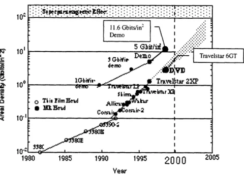
1-1 Growth of areal density in hard disk drive ... 2
2-1 (a) Sectioned diagram of perpendicular patterned media and a single pillar magnetized in N direction (b) Hysteresis loop of a single magnetic domain pillar in its long axis ... 15
2-2 (a) Face Centered Cubic (FCC) crystal structure (b) Hexagonal Close-Packed crystal structure ... 16
2-3 Experimental setup for the switching field measurement ... 19
2-4 Detailed diagram of the experimental setup ... 21
2-5 The layout of the test sample (s = 150 nm, 200 nm, 250 nm, and 300 nm for pillar arrays, s = 1,500 nm for isolated pillars) ... 24
2-6 SEM image of the Ni pillar arrays ... ... 27
2-7 The dimension of the pillar ... 31
2-8 (a) Experimental hysteresis loop of a single Ni pillar (90 nm x 180 nm) (b) MFM imag at H = 580 Oe (c) MFM image at H = 620 Oe ... 32
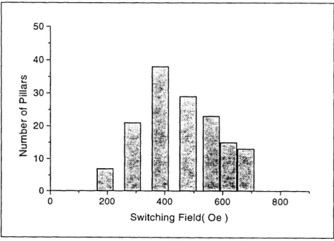
2-9 Switching field distribution of 300 nm Ni pillar array ... 33
2-10 Switching field distribution of 300 nm, 250 nm, and 200 nm period arrays ... 35
2-11 Switching field distribution of the arrays with different pillar heights ... 36
2-12 Switching field distributions of Ni pillars with identical size (90 nm x 180 nm), m easured from 300 nm array ... 42
2-13 Switching field distributions (a) 300 nm pillar array (b) table for color - switching field range ... 43
2-14 Large crystals in Cobalt pillar array with 200 nm spacing ... 45
3-1 Scheme of writing with magnetic force microscope ... 49
3-2 MFM images of 6 x 6 Ni pillar arrays of various spacing before and after PMR writing. The pillar in the dotted box is the target pillar. ... 56 3-3 Schematic of writing field measurement (a) Coil field (Hcoil) applied to the pillar when the switching occurs without MFM probe near the pillar (b) with MFM probe
3-6 Hysteresis loop of the MFM probe input to the simulation software ... 62
3-7 Simulation results of writing field during PMR process ... 64
3-8 Magnetic field distributions around the tip ... 65
4-1 Schematic of interaction field between the pillars ... ... 70
4-2 3 x 3 pillar array with spacing S where the interaction field applied to Pillar 5 by the surrounding eight pillars is studied ... 72
4-3 The target pillar is switched at the coil current of Ic = 0.4 A. Refer to Appendix A for real MFM images. ... 77
4-4 The target pillar is switched at I, = 2.2 A. ... 78
4-5 Magnetic state of the pillars in 250 nm period array before and after the writing field is applied. (a) The state of the center pillar is switched at Ic = 2.2 A. (b) The switching occurred at I = 2.7 A. Here, the tip is magnetized in the opposite direction. ... 80
4-6 Magnetic state of the pillars in 200 nm period array before and after the writing field is applied. (a) The state of the center pillar is switched at I = 2.4 A. (b) The switching occurred at Ic = 3.4 A. Here, the tip is magnetized in the opposite direction. ... 80
4-7 The experimental and simulation data of interaction field between two pillars as a function of distance between the pillars ... 86
5-1 Four key design components that determine the overall speed of MFM based data storage system ... 96
5-2 (a) Multiple tips with micro-actuator for vertical motion and macro-actuator for tracking and accessing motion (b) The area covered by one single recording head ... 102
5-3 Schematic of the cantilever with integrated sensor and actuator (a) Top view (b) Side view ... 107
5-4 (a) The FEM model of the actuation part of the cantilever; number of nodes: 3834; number of elements: 948; 1s' mode natural frequency: 475 kHz; 2nd mode natural frequency: 671 kHz. (b) The sensing part of the cantilever; number of nodes: 1223; number of elements: 310; 1st mode natural frequency: 507 kHz; 2nd mode natural frequency: 1.76 MHz. (c) The whole cantilever; number of nodes: 3433; number of elements: 852; 1s' mode natural frequency: 265 kHz; 2nd mode natural frequency: 622 kHz. ... 110
5-5 The tracking motion of the tip with respect to the sample surface ... 113
5-9 Effect of noise ... 119
5-10 Effect of the radius of tip motion ... 121
5-11 Effect of step size ... 122
1.1 Introduction
Recently, demands for the high performance data storage devices have been increasing rapidly due to the advent of new digital technologies such as high definition television (HDTV), global networks and high performance microprocessors. The magnetic recording industry now has annual revenues of 100 billion dollars and employs of over 500,000 people. The market is projected to grow continuously in the next decades. Such success in the data storage market brought about highly competitive atmosphere among the researchers in this field. This is well indicated in the recent growth of recording density of hard disk drives (HDD) [1]. Figure 1-1 shows the trend of the density growth during the recent two decades. According to the figure, the density has grown at a compound growth rate (CGR) of 60% increase per year in recent 10 years. Such trend appears shortly after the introduction of the magnetoresistive (MR) recording heads in 1990. This shows that the performance of the recording heads was the key design factor in increasing the recording density at that time. Recently, the recording density of 11 Gbits/in2 was demonstrated in the
laboratory and the commercial HDD products 3 Gbits/in2 in recording density are now
available'. According to the rate, the demonstration of 100 Gbits/in2 will be possible by the
year 2004.
Will the recording density of 100 Gbits/in2 be ever possible? In order to discuss
m
r
,t
P1
Vear
Figure 1-1 Areal density growth of the hard disk drives
this issue, we should examine the three main components of a HDD, namely recording media, recording head and positioning system. The recording media used in current HDD's are the thin film media, usually cobalt based alloys deposited on a substrate. The limiting factor of such media is the media noise. As the bits become smaller, their magnetic fields are reduced till they are finally overtaken by the random nature of the grains. In order to reduce the bit size while retaining a decent signal to noise ratio, the size of the grains should be reduced as well. However, if the grains become too small in size, the grains become thermally unstable at a normal room temperature. This is known as the superparamagnetic limit. The critical size of the grains can be estimated for various materials [2]. For the spherical Co grains, the critical diameter is about 10 nm and for the Ni grains, it is about 30 nm.' If the individual bit consists of 1000 grains to cancel out the random effect of the grains, the diameter of the bits becomes 100 nm for Co and 300 nm for Ni. These are the minimum sizes of the bits that can be recorded in thin film media. For the
1 We used the equation of the magnetization reversal rate, which is a function of the anisotropy constants,
temperature and volume of the grain. In the calculation, the relaxation time of 100 seconds was assumed for the superparamagnetic effect.
Co thin film media, the number indicates that the recording density can be increased up to 65 Gbits/in2 before it meets the superparamagnetic limit.
The recording head technology had a notable progress in recent years. According to Figure 1-1, MR head technology was the main drive of the recording density growth in 1990's. The giant magnetoresistive (GMR) technology is now successfully implemented in commercial hard disk drives. The recording density of the systems using these heads was up to 11 Gbits/in2. Currently the sensitivity of these heads is about 2 times higher than that of MR heads and projected to increase higher. The increased sensitivity makes it possible to detect smaller recorded bits and to read these bits at higher data rates. For a higher recording density, the thickness of GMR sensor should be reduced to the required size, usually smaller than the recorded bit length'. Currently, the fabrication of GMR heads that meet such requirements is a challenging task.
The positioning system is responsible for precise positioning of a recording head on a specified track. During a read/write process, the recording head slides on the top of a spinning disk, following the concentric circular data tracks. A small gap between the head and the disk is kept by a thin air film, generated by a rapidly spinning disk. Currently, HDD has a low track density due to its flexible structure that holds the head. A two-stage microactuator is proposed to achieve a higher track density.
The general notion is that the most critical component, limiting the areal density of 100 Gbits/in 2, is the recording media. The superparamagnetic limit of thin film media will probably limit the density higher than 50 Gbits/in2.2
Optical data storage had also a notable progress in recent years. Recently, the digital video disk (DVD) is introduced in the market. The system reportedly has the areal density of 3.28 Gbits/in2. See Figure 1-1 for the comparison. Such high recording density
1 The recorded bit length for the recording density of 2.6 Gbits/in2 is about 120 nm.
was achieved because the system can provide a good signal to noise ratio down to very narrow track widths. This is possible because the optical system can afford a large working distance between the head and the media. It doesn't require a tight control of the gap as in the case of HDD. However, there are a few technical difficulties for the higher recording
density applications. To detect smaller bits, an optical source with shorter wavelength should be used. Currently a semiconductor laser in a blue-purple range, stable at room temperature, is being developed but the performance vs. cost did not yet reach the proper level for commercial products. Near-field optical scanning microscope (NSOM) is another approach to increasing the detection capability.
The concept of patterned media is introduced to overcome the limitation of thin film media. The patterned media consist of periodic arrays of single domain magnetic particles fabricated using current lithography technology. Each particle is used to store one bit of data. The advantages of such media are well recognized. First, the patterned media can be a solution to overcome the superparamagnetic limit of thin film media. In thin film media, because the size and the orientations of the grains in a bit are random in nature, the signal to noise ratio (SNR) of a magnetic signal from each bit increases as the number of grains in each bit increases and therefore it averages out the effect of individual grains. As a result, to reduce the bit size while maintaining the same level of SNR, the size of grains must be reduced. There is a limit, however, in reducing the size of the grains, known as the superparamagnetic limit. At this scale, the grains are weakly coupled to each other by an exchange force so that the energy required to switch the magnetization of a grain becomes smaller than the thermal fluctuation at room temperature. As a result, all written bits are erased. In patterned media, each bit is stored in a spontaneously magnetized single domain particle, having two stable magnetic states. Since current thin film media requires bits to have 1000 grains for the adequate SNR, making the bit stored in a grain promises a 1000 times increase of a recording density.
Secondly, the patterned media do not suffer from the transition effect between neighboring bits. In thin film media, when a bit is placed next to another bit magnetized in opposite direction, a transition, called domain wall, must be formed to reduce the exchange energy. The spacing between two bits cannot be smaller than the width of the domain wall. Also, to minimize the total energy consisting of the magnetostatic force and exchange force, the transition area between two bits becomes a random zig-zag shape, called Neel spikes. Such shape can become a significant noise source in read back signal. The transition width in current thin film media runs between 40 nm and 80 nm. In patterned media, there is no transition area existing between bits, because the bits are separated by non-magnetic materials.
Thirdly, the patterned media do not have the side track problem. In thin film media, the fringing field generated at both sides of a write head creates the garbage next to the data track and therefore an extra space should be provided between the two data tracks. This limits the recording density in the radial direction.
Another advantage of the patterned media is that it provides a self tracking signal. In conventional media, the tracking is a blind motion since there is no physical boundary between the two bits when they have the same magnetization direction. Therefore the tracking must rely on the data recorded solely for the purpose of tracking. This method would not only require an accurate servo and a disk spindle motor but also use up 20% of disk space for the tracking data.
The main focus of this thesis is to design a data storage system with an extremely high recording density beyond 100 Gbits/in2. We start from the characterization of the media property to prove and demonstrate the advantages of the patterned media in high recording density data storage. We pursue this issue further to discuss the design of an actual system based on this concept using a high resolution magnetic imaging technique called magnetic force microscopy.
1.2 Historical Review
The advantages of the patterned media were first discussed in the study of discrete track media [4-6]. Lambert et al showed that patterned track on the media can suppress the noise problems and allow a narrow track width [4][5]. Early works of fabrication and characterization of the array of submicron patterned magnetic particles were presented by Smyth et al. [7][8]. In their studies, the arrays of permalloy particles at an areal density of 160 Mbits/in2 were fabricated by using electron beam lithography. The collective behaviors of the particles were examined with alternate gradient magnetometer (AGM). The effects of the particle size, aspect ratio, and angular dependence on the hysteresis loop parameters were studied. It was shown in their papers that the coercive force of the patterned media is much higher than the film media of the same thickness along the long axis of the particles. Schultz et al. conducted further analysis on the patterned array by using magnetic force microscope (MFM) which enabled them to observe the properties of the individual particles [9-15]. The array of permalloy bars with the size of 130 nm x 50 nm x 1,000 nm at an areal density, ranging from 220 Mbits/in2 to 1 Gbit/in2 were fabricated and observed with an MFM. The investigations on the switching and interaction properties of the individual particles indicated that those particles are single domains. Also, they experimentally showed that the single domain particles at such densities are actively interacting although they failed to provide quantitative data. Later, O'Bar et al. from the same group investigated the switching properties of the isolated Ni columns 120 nm in diameter and 1,400 nm in length, using an MFM and an electromagnet [12-14]. They showed that the magnetization state of the column is always in one of two equivalent, but opposite polarity states, even when the applied field was near the saturation field of the column, thus the column can be considered as a single domain. The authors also examined the relationship between the switching field and the angle of the applied field and also the switching field
and the size of the particles. They found that they agree well with the curling mode.
More experimental works have been conducted by Chou et al. [16-19]. They fabricated the arrays of Ni pillars 50 nm in diameter and 200 nm in height with an areal density of 65x109 pillars/in2 using electron beam lithography. The magnetic properties of
the pillars were observed with MFM. They examined the switching and interaction properties of isolated Ni and Co bars with a wider range of geometry. The Ni/Co particles with a thickness of 35 nm and a length of 1,000 nm were observed as their width varied from 30 nm to 300 nm. Also, the switching properties of the particles, 100 nm in width and 35 nm in thickness, were observed as the length varied from 100 nm to 5,000 nm. Their results showed that the pillars follow the behavior of both the multi-domains or single domain and therefore had different switching mechanisms.
White et al. provided important theoretical works regarding the patterned media [3][19-23]. They have fabricated arrays of single domain Co/Fe particles with electron beam lithography and studied the effect of magneto-crystalline, surface and shape anisotropy on the magnetic states and easy axes [20][23]. They theoretically showed that, for small size hard magnetic particles, it is difficult to have a predictable and well-defined easy axis and switching properties. They, also, showed that [110] single crystal iron thin film has a strong uniaxial surface anisotropy and an easy axis of magnetization lying in the
[001] direction, regardless of the particles' shape, suggesting a new approach to making of
the particle arrays with uniform magnetic properties. Shi et al. have also fabricated single domain ferromagnets in GaAs with ion implantation and subsequent heat treatment. They studied the property of the sample with MFM under the varying external magnetic field [24][25]. Fernandez et al. fabricated arrays of Co dots with spacing of 300 nm using interferometric lithography [26-28]. Later, the fabrication of 200 nm period pillar array with interferometric lithography was reported by Farhoud et al. [30]. The potential applications to the fabrication of the particle array with a period of 100 nm and below are
explained [31]. This method has been proven to be a good candidate for the mass production technology.
1.3 Thesis Outline
Chapter 2 discusses the switching properties of the patterned media. The experimental measurements were performed on the Ni nano-pillar array with a small period, 150 nm -300 nm. A commercial MFM and an electromagnet were used to determine the switching field of each individual pillars, 90 nm in diameter and 180 nm in height. Based on the results, the single domain behavior and the switching mechanism for these pillars are discussed. This chapter also discusses the variations of the switching field for the pillars with nearly identical size, which may be critical in data storage applications. Chapter 3 discusses a possible read/write method for the high density perpendicular patterned media using magnetic force microscopy. We found that this method could readily write on the pillar array with a period of as small as 200 nm. The resolution of this technique depends on the shape of the tip and is expected to write bits with size comparable to the radius of curvature of the MFM tip, currently in the range of 30-50 nm. Chapter 4 discusses the magnetic field interactions between the pillars. The experimental method of measuring the interaction fields between individual pillars is proposed and explained. A key factor in this method is to keep the adjacent pillars in the same magnetic state during the measurement of the interaction field applied to the selected pillar. This is possible with writing method -described in Chapter 3. With this method, we could measure the interaction fields between the pillars with spacing as small as 200 nm, 250 nm, and 300 nm, much smaller than previously reported. The experimental data are compared with the theoretical values calculated from the dipole approximated magnetostatic equation. Chapter 5 discusses a design of the data storage system based on the magnetic force microscopy. First, the current
performance of HDD is reviewed to determine the required specifications of the proposed system. Next, the design and the possible performance of the system based on the parallel operation of MFM recording heads are described. Calculations on various performance parameters were performed to ensure that the proposed design could become a viable high density data storage system.
2.1 Introduction
Coercivity is one of the key properties in the studies of fine magnetic particles. The reason is that, first, it must be sufficiently high for the particles to be of use in recording applications and it is a property, which can be naturally obtained from the computed hysteresis loop. In the case of patterned media where each bit is stored in a single domain particle, coercivity is the field that switches the magnetization direction of the particle from one state to the other state. It is also known as the switching field. The goal of this chapter is to investigate the switching properties of single domain magnetic particles in patterned media. Possible mechanisms of magnetization switching are studied by evaluating important theoretical models suggested by researchers such as Wohlfarth [32] and Frei [33].
The test samples were fabricated in the Nano-Structures Laboratory headed by Professor H. I. Smith and in the laboratory of Professor C. Ross. The samples were fabricated for the purpose of fundamental experimental characterizations on the patterned media. There were several key issues concerning a design of the samples. First, the long axis of each particle was along the axis, out of sample plane and therefore the particle has an easy axis of magnetization along that direction due to a shape anisotropy. Such particle is also called a nano-pillar or simply a pillar. The thin film media with the same axis of magnetization, called perpendicular media, have gotten attentions because it allows theoretically higher recording density than that of conventional longitudinal media. The recording density of the test samples was as high as 3x1010bit/in2, which is about 3 times
higher than that of current hard disk drives. Such density was chosen because this density is close to the known range of superparamagnetic limit.
Section 2.2 reviews the crystal anisotropy and a shape anisotropy, which fundamentally affect the switching properties of the pillars. Section 2.3 describes the experimental procedures and results of the measurements performed on individual pillars. This section studies in depth of the single domain behavior of each pillar and the relationship between the switching field and the geometry of the pillar array. Section 2.4 discusses theoretical models that describe the switching behaviors of the same pillars studied in previous sections. A recent trend is to calculate the switching field with a micromagnetic simulation software. Immense calculations involved in micromagnetic simulation have been possible due to the rapid development of computers. Many papers addressing the computation methods of these models have been published [34-41]. This thesis, however, takes simpler approaches, which use theoretical models based on a fundamental driving physics. A model that best describes the experimental behavior of the pillars was used to show the dependence of the switching field on the geometry and the material of the pillars. Section 2.5 discusses the variations of the switching field observed
in the array where the pillars have nearly identical geometry.
2.1.1 Background
Studies of the magnetization reversal process of nano-scale ferromagnetic particles both in theory and experiment have been of interest to many researchers. A calculation of the field that rotates the Ms vector of a single domain particle out of its easy axis were performed by using micromagnetic computer simulations [34-41]. In these simulations, it was assumed that the rotation was taking place against the restoring force of some anisotropy, usually the anisotropy of shape, stress, or crystal, which depend on the shape, size, roughness and
materials properties of the particle. This aspect was also investigated by using experimental methods. Chou et al. studied the effect of a shape anisotropy on the switching field of nano-scale single domain particles by using a magnetic force microscope [16][17]. It was shown in their work that when the length of Ni bars 100 nm in width and 35 nm in thickness was increased from 500 nm to 1000 nm, the switching field increased from 450 Oe to 640 Oe, following a model of coherent switching. But, when the length was increased from 1000 nm to 5000 nm, the switching field decreased from 640 Oe to 400 Oe, showing an incoherent switching behavior. Schultz et al. [12][13] performed similar experiments. Their group showed that a Ni column of 1400 nm in length and 120 nm in diameter followed a curling mode behavior. White et al. investigated the effect of surface anisotropy in single crystal iron particles and found that the surface anisotropy was stronger than the shape anisotropy in these particles, so that the easy axis of magnetization lied in the [001] direction regardless of the shape of the particles.
Numerous fabrication techniques for the arrays of nano-scale ferromagnetic particles were introduced. Two-dimensional assemblies of magnetic wire or rods were made by deposition inside holes in a polymer membrane [42-44] or through pores in anodized aluminum [11][13-15]. These techniques allowed large area samples with densities up to 1011 bit/cm2 and the pillar height as large as several microns. However, the spacing between the bits was random or semi-random in the case of alumina pores, making it difficult to model and to take measurements of the properties. Electron beam lithography was used by numerous researchers because it could produce particle arrays with precise dimensions and various patterns. Chou et al. fabricated high density magnetic pillar arrays with a period of 100 nm in Co or Ni by electroplating through photoresist exposed with electron beam lithography [45-47]. Interferometric lithography (IL) had recently been applied to the fabrication of nano-magnet arrays over a large area. A 300 nm period IL system was demonstrated by both Fernandez et al. [26-28] and Kirsch et al. [48] for making
arrays of magnetic dots using an evaporation and lift-off process. Farhoud et al. used electrodeposition technique to make higher aspect ratio pillars in Co and Ni with periods of 200 nm and heights up to 400 nm [30].
In this thesis, the electron beam lithography technique was used to build the array of nano-scale single domain pillars with a range of sizes and spacings. The thesis investigates the magnetic behavior of the pillars with size and spacing smaller than those previously reported. The Ni Pillars with a diameter of 90 nm, a height ranging from 130 nm to 180 nm, an spacing ranging from 150 nm to 300 nm (7 Gbit/in2-30 Gbit/in2) were fabricated and their magnetic properties were investigated.
2.2
Fundamental Concepts
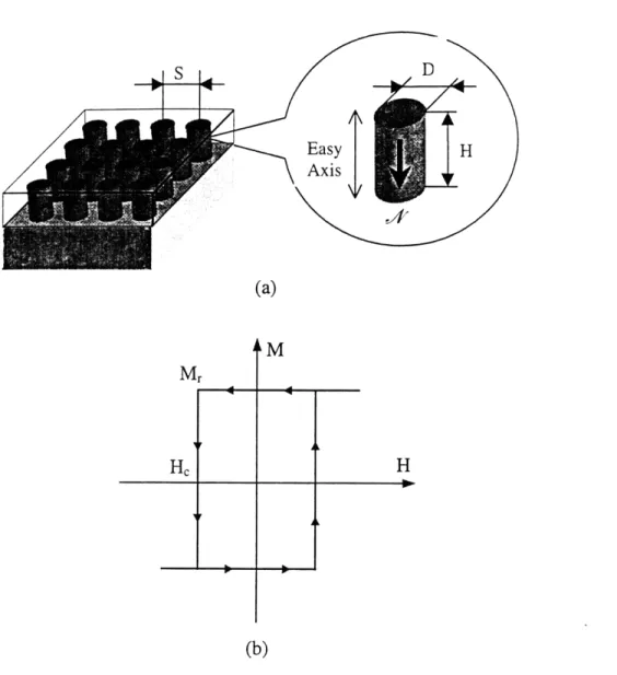
Figure 2-1 (a) shows a diagram of perpendicular patterned media. The media consists of single domain magnetic pillars evenly embedded in a nonmagnetic filler. The orientation of the pillars' main axis is perpendicular to the surface of the medium. In the figure, the distance between the pillars is represented as S, constant for all pillars in the array. Figure 2-1 (b) shows the picture of a single pillar. The shape of the pillar is a cylinder with diameter, D, and height, H. The aspect ratio of a pillar is simply H divided by D.
Due to their size and aspect ratio, the magnetic pillars in the patterned media are assumed to be single magnetic domain in character'. As a result, the shape anisotropy forces the magnetization along the main axis of the pillar. A single domain particle in theory is spontaneously magnetized to the saturation magnetization, Ms, along a preferred axis of magnetization, called an easy axis. It has, therefore, only two stable states, equal in magnitude but opposite in direction. The switching process of single domain pillars can be explained with a hysteresis loop, shown in Figure 2-1 (b). If an external field is applied to
(a)
Mr
(b)
Figure 2-1 (a) Sectioned diagram of perpendicular patterned media and a single pilla magnetized in N direction (b) Hysteresis loop of a single magnetic domain pillar in it long axis
the pillar along its main axis and increased to He, the magnetization of the single domain pillar is not reduced to zero but instantly reversed to the other state.
The switching field, denoted as Hc in Figure 2-1 (b), is defined to be the magnetic field needed to reverse the magnetization of a single-domain element from one direction to the other. Among the factors that affect the switching field strength and the easy axis of the
L
M 44 - 4
(Easy Axis) Axis )
(Hard Axis)
(a) (b)
Figure 2-2 (a) Face centered cubic (FCC) crystal structure (b) Hexagonal closed-packed crystal structure
single domain particles, magnetocrystalline anisotropy' and the shape anisotropy are the most important ones. The magnetocrystalline anisotropy, also called crystal anisotropy, is due to the crystal structure, forcing a certain crystal direction to be an easy axis. The shape anisotropy originates from the shape of the particle. When this factor is dominant, the easy axis aligns with the long axis of the particle.
Magnetocrystalline anisotropy is mainly due to the spin-orbit coupling. The magnetization is due to the electron spin of the atoms. When the external field tries to reorient the spins and therefore to change the magnetization, it is resisted by strong coupling between the spin and the orbit, again strongly coupled with the crystal lattice. As a consequence, the magnetocrystalline anisotropy energy required to rotate the spin is the energy required to overcome the spin-orbit coupling. The strength of an anisotropy in any
particular cubic crystal is experimentally determined by the magnitude of the anisotropy constants, KI and K2. Nickel has a face centered cubic structure and the easy direction, from experiment, is known to be <111> direction. The crystal coordinates and the easy axis of single crystal Nickel is shown in Figure 2-2(a). The equation of crystal anisotropy energy for Ni is
S= K + K,(a2 a2 a+ a a + a2a 2
1 )+K 2(C2 af)+A (2.1)
where al, a2, and a3 are defined as the cosines of the angles between the magnetization vector and each of the crystal axes. The easy axis is along the magnetization direction at which the energy, E, in Eq. (2.1) is minimum. Co, on the other hand, has a hexagonal closed packed structure as shown in Figure 2-2 (b). In such a structure, the hexagonal c axis is always the direction of easy magnetization and any direction in the basal plane is found to be equally hard to magnetize. In this case, the crystal anisotropy energy only depends on one angle, 8, between the magnetization vector and the c axis.
The shape anisotropy is due to the shape of a magnetic structure. If the structure is spherical in shape, there is no preferred direction of magnetization due to the shape effect. But, for a non- spherical structure, it's easier to magnetize along the long axis than the short axis. For the quantitative representation of the shape anisotropy energy, the anisotropy constant, Ks, is given by
1
K, =(Na-N)M 2 (2.2)
where Na is the demagnetizing factor along the short axis and N, is the demagnetizing factor along the long axis for the axially symmetric case. The strength of a shape anisotropy depends on the aspect ratio of the structure, which determines the term ( Na - Nc) in Eq. (2.2) and the magnetization M [2]. For the case of single domain particles, M is equal to Ms, saturation magnetization.
Shape anisotropy and crystalline anisotropy are the most contributing factors that determine the switching properties of the single domain particles. But as is often the case, the one is dominant over the other and responsible for the magnetic behaviors of a particle. The switching field and the easy axis of a pillar can be estimated from the anisotropy energy equation of the dominant anisotropy energy.
2.3 Switching Field Measurement
In this section, we present the results of the switching field measurements, performed on the nano-pillar arrays with various geometries. First, the experimental setup, test structures, and experimental procedures are described. The next part presents the experimental results of the switching field measurements. These include the hysteresis loop of a few selected pillars and the graphs showing the switching field properties.
2.3.1 Experimental Setup
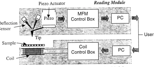
Figure 2-3 shows the experimental setup used in the switching field measurement. The setup can be divided into a writing module and a reading module as depicted in the figure. The reading module checks the magnetization state of the pillars at each time a field is applied. The writing module applies specified magnetic fields to the pillars under observations. For our case, the field should be applied along the pillar's long axis, perpendicular to the media surface.
The reading module must meet the following requirements.
* The sensitivity should be high enough to detect a weak flux from a single pillar. Nickel pillar, 90nm in diameter and 180 nm in height, the magnetic moment, available for the
-
User
Writing Module
Figure 2-3 Experimental setup for the switching field measurement
sensor is only about 5.53X101 3 emu.
* The spatial resolution of the sensor should be in the order of nano-meters. Such resolution is needed to observe the magnetic pattern of the pillars.
The magnetic force microscope (MFM) meets these requirements well by providing high field sensitivity and an excellent spatial resolution. The MFM is a scanning probe microscopy (SPM) techniques, which uses a fine probe and high resolution actuators to measure extremely small quantities of surface properties. The main purpose of these instruments is to measure the surface topography in an atomic scale resolution. The MFM uses a probe coated with magnetic material to image the magnetic patterns on the sample. During the imaging, a probe consisting of a sharp tip and a flexible cantilever is oscillated near the sample surface and moved along the sample surface while the distance between the tip and sample is kept constant. At the same time, the shifts in resonant frequency are monitored by measuring the phase of the cantilever's oscillation relative to the drive signal. The phase change measured at each location on the sample constitutes a data set that can be mapped to the magnetic force gradient image of the area. The tip-sample distance for MFM
imaging is about 100nm, long enough to avoid the effect of van der Waals force'. The resolution of MFM depends heavily on the quality of the tip. Currently, for a normal MFM mode, the resolution is about 10 Onm.
Other similar instruments for the imaging of nano-scale magnetic domains include Lorentz microscopy [49-50], electron holography [51][52], and spin polarized scanning electron microscope [53]. These techniques have comparable resolutions but require a cumbersome vacuum process.
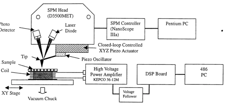
Figure 2-4 shows the detailed description of the experimental setup used in the switching field measurement. A commercial MFM, Dimension 3500 by Digital Instruments, was used as a reading module. In the system, a piezoelectric scanner consisting of piezoelectric stack and flexures is used to position the probe to required locations. The moving range of the scanner is approximately 90 pm in horizontal direction and 6 pm in vertical direction. The scanner is closed-loop controlled in all three directions and maintains the resolution down to 1 nm2. Such a feature removes the effect of the hysteresis and creep behavior, usually observed in piezoelectric actuators, and allows more accurate and faster imaging. The system also has a separate piezoelectric actuator for the oscillation of the cantilever and a lock-in amplifier for AC detection imaging. These components are needed in MFM and Tapping mode scan3. The D3500 has an XY stage for the
macro-positioning of the sample and a vacuum chuck for fixing of the sample. In our setup, the vacuum chuck is used to hold both the coil and the sample. See Figure 2-4.
•1 MFM measurement usually runs in two scans per line. In the first pass, the topography is
measured near the sample and, in the second pass, the magnetic force gradient is measured at some lifted height above the sample topography. This is to remove the effect of the topography in the magnetic measurement.
2 Note that the resolution in vertical direction during contact AFM mode is much higher than 1 nm since the atomic force data sensed by the cantilever is used to control the vertical motion of the tip.
3 Tapping mode, patented by Digital Instruments, is one of the AFM imaging techniques. During
the imaging, the cantilever oscillates while the tip lightly touches the sample surface. The amplitude of the cantilever oscillations are monitored and mapped into the topographic image.
Photo Detect
Test Saml Coil
XY s
Figure 2-4 Detailed diagram of the experimental setup
In our experiments, two types of MFM probes were used, the standard probe and the low moment probe. We found that the standard probe affects the magnetization of the sample during the imaging. The stray field from these probes was strong enough to affect the states of pillars. Low moment probes were used for most of the switching field related experiments. It has a thinner magnetic coating on the tip and therefore a lower field strength. The spatial resolution of the MFM was improved since the radius of curvature of these tips is smaller'. However, due to a small magnetic volume on the tip, the sensitivity of the probe was reduced and consequently, the contrast of the MFM image was lowered.
A common method to realize the writhing module is to use an electromagnet. The following is the design criteria for the electromagnet to be used in our application.
1 According to the manufacturer's data, the radius of curvature for the standard tip is 25-50 nm and 20-40 nm for the low moment tip.
* The range of magnetic field that can be generated from the coil should cover at least -1000 Oe Hext 1000 Oe
* The rise time of the field in response to the current step input should be shorter than a few mili-seconds.
* The coil or other experimental components located near the sample during the measurement should not interfere with MFM imaging. Non-magnetic materials are preferred for these components.
* The size of the coil should be small enough to fit inside the MFM platform. The height of the coil should be smaller than 2 cm. Maximum allowable distance between the tip and the sample stage in D3500 is about 2.5cm
The coil used in our experiments can generate a magnetic field as high as ±1000 Oe. The shortest pulse it can produce was around 3 msec. A plastic bobbin was used for the coil base instead of the common magnetic ferrite core because it had been reported that the latter type of core seriously degrades the MFM imaging. Because we used the plastic base, we needed a high current of 12 A supplied to the coil in order to meet the requirements. Producing a current pulse of 12 A with duration as short as 3msec was a difficult task because of the high inductance of the coil and the high capacitance of the amplifier circuit. Table 2.1 shows the final specifications of the coil used in our experiment. The detailed design process and the specifications of other test coils are provided in Appendix B. Note that the actual field generated from these coils was measured with a commercial gaussmeter. The measured data, input current vs. coil field, are provided also in Appendix B. As depicted in Figure 2-4, the coil was fixed between the sample and the stage and held by the vacuum chuck. This orientation enables the coil to directly apply a field vertical to the sample and, at the same time, the MFM probe to scan across the sample. The power amplifier' was used to produce a current pulse with amplitude ranging from -12A to 12 A.
I
\
I
Table 2.1 Specifications of the coil
The shortest pulse the amplifier and the coil can produce has a width of 3 msec. The amplitude and the duration of the current pulses were set by the digital signal processing (DSP) board through the programming input port of the amplifier
In summary, our experimental setup consists of the coil and a commercial AFM/MFM instrument. Fields ranging from -1000 Oe to 1000 Oe can be applied vertically to the sample and the resulting magnetic state of the sample can be monitored by MFM imaging.
2.3.2 Sample Fabrication
The samples were fabricated for the study of various media properties. Two properties of most interest were the switching field and the interactions. The dimensions of the pillars were chosen so that they were within the predicted range of a single magnetic domain. Pillar arrays with 150 nm, 200nm, 250nm, 300nm, and 1,500nm in spacing were fabricated.
Number of Turns 150
Size( D, h ) 8.6 [mm], 6 [mm]
Wire A.W.G. Size 29
Resistance of Wire 81.22 [0/1000 ft.]
Time Constant 68 [sec]
Maximum Field ±1000 [Oe]
!
fh
' '
-T cm
1
cm
A Test Sample 000000000000000000 00000000000000000000 00000000000000000000 0000000000000000000 00000000000000000000 00000000000000000000,, 000000000000000000 0000000g00000000000 000000000000000000 00000000000000000000 0000000000000000000 00000000000000000000 0000000000000000000 0000000000000000000 00000000000000000000 000000000000000000 0000000000000000000 00000000000000000000 00000000000000000000 0000000000000000000 20 x 20 MatrixFigure 2-5 The layout of the test sample ( s = 300 nm, 250 nm, 200 nm, and 150 nm for pillar arrays, s = 1,500 nm for isolated pillars )
The pillar arrays with various spacings allow the study of the interaction field as a function of the distance between the pillars. The pillar arrays with 1,500 nm in spacing were intended for the study of completely isolated magnetic particles. All the samples used in these experiments were fabricated at the Nano-Structures Laboratory in the Department of Electrical Engineering and the laboratory in the Department of Material Science at MIT'. The following summarizes the features of the test sample design.
* Each pillar has the aspect ratio of more than 1 and therefore it's assumed that the shape anisotropy forces the easy axis to be in the main pillar axis, vertical to the sample surface. The perpendicular patterned media were of most interest in this thesis because it theoretically allows a higher recording density than the conventional longitudinal
' The author credits May Farhoud, Mark Mondol, and Minha Hwang for their support on the
media.
* The smallest spacing of the pillar array is 150 nm. If each pillar stores one bit of data, the array has the recording density of nearly 30 Gbits/in2. The areal density of the hard disk drive has now passed the 10 Gbits/in2 mark. Such rapid increase in recording density is getting very close to the superparamagnetic limit, expected to occur around the 30-50 Gbits/in2 range.
* Both Ni and Co are used for the pillars. However, most of the experiments are performed on Ni pillars because the Co pillar arrays showed such wide variations in switching field, making it impossible to pursue further analysis.
The fabrication process included electron beam lithography and electroplating. The reason for using electroplating rather than the lift-off process was that it easily produced high aspect ratio vertical structures. The following summarizes the fabrication procedures.
1. Deposition of an electroplating seed layer
100 A of Ti and 200 A of Au were evaporated on to the 3 " bare silicon wafer. A conductive Au layer was used as a seed layer for the electroplating of Co and Ni.
2. Spin coating of a photoresist
The positive resist, 3% PMMA of 950 K molecular weight, was spun onto the substrate. The resulting thickness of the PMMA layer was around 250nm. Because the plating material eventually fills up the holes on PMMA template and constructs the pillars, the thickness of the PMMA layer determines the final height of the pillars. The empirical plot of a spin curve, the thickness of PMMA vs. spin speeds, was used to predict the correct speed for the target thickness.
3. Electron beam lithography
The patterns, shown in Figure 2-5, were exposed on the PMMA using an electron beam lithography technique.
4. Flood exposure.
In order to predict the plating rate, the area outside the 1 cm x 1 cm region where the test patterns were written was exposed with a flood exposure system. The area was later plated simultaneously with the test pattern. The plating rate inside the test pattern, then, was estimated based on the known area outside the pattern, The whole wafer with test structures covered with a piece of aluminum was exposed to the UV light for about 15 minutes.
5. Develop
The exposed PMMA was developed in MiBK:IPL=2:1 solution for 45 seconds. 6. Reactive Ion Etching (RIE)
By using the RIE, the remaining PMMA and other possible contaminants on the surface of the plating layer were removed.
7. Electroplating
Ni was deposited from sulfamate electrolyte with a plating temperature at 500C. The
solution contained 327 g/l of anhydrous nickel sulfamate, 30 g/l of boric acid, 3 g/l of a properietary anode corrosion aid and 0.3% by volume of wetting agent. Boric acid was used to adjust the pH to 3.6. Co was deposited from either a sulfate or a sulfamate electrolyte. The sulfate solution contained 200 g/l Co sulfate, 30 g/l cobalt chloride and 30 g/l boric acid with pH of 3.5. The sulfamate solution contained 75 g/l cobalt and 45 g/l boric acid, and the pH was in the range of 3.5 to 4.5. The plating rate was controlled by the plating current density, ranging from 1 to 11 mA/cm2, but was very sensitive to the conditions of
(a) 150 nm Pillar Array
(c) 250 nm Pillar Array
rV W W wwo WW W %w
000000000
(d) 300 nm Pillar Array
Figure 2-6 SEM image of the Ni pillar arrays
8. Inspections
The PMMA template was removed in the acetone bath to leave the pillar array, ready for the inspection. The resulting test patterns were observed with the scanning electron microscope (SEM).
The SEM images for the Ni pillar arrays with 150 nm, 200 nm, and 300 nm in spacing are shown in Figure 2-6. The average diameter of the pillars in these arrays was 90 nm. The diameter was measured based on the known spacing between the pillars. The height of the pillars was measured with AFM. The height ranged from 130 nm to 200 nm for the samples plated at different conditions. It was known that the height of the pillar depends on the plating time, input current density, temperature, etc, but the accurate prediction of the plating rate was difficult, probably due to some unknown plating
aw "r 1W or
'i
i
(b) 200 nm Pillar Array * 4 i~ i~ 4 j; 0 0 AVparameters. The shape of the pillars in Figure 2-6 (d) indicates that the electron beam is not perfectly stigmatized. This, however, is not significant enough to induce the shape anisotropy in such a direction.
In summary, the electron beam lithography and electroplating were used to fabricate the arrays of Ni pillars having a diameter of 90 nm, a height of 120 nm - 200 nm and spacing of 150 nm - 300 nm. The electron beam lithography system provides a flexible and easy way to make small structures, but its inherent scanning method results in slow throughput. A different approach using the interferometric lithography is currently developed at the Nano-Structure Laboratory as a mass production technology of the patterned media [30][31].
2.3.3 Experimental Procedures
The switching field of the pillars was measured following the procedures described below. 1. Initial magnetization of the sample and the MFM tip
First, the sample was placed at the center of the coil shown in Figure 2-4 and secured with a vacuum. A visible mark was made on the sample to indicate the location of the patterns. First, the sample was magnetized along the pillar axis under a field of 3000 Oe. The MFM tip, fixed in the microscope, was magnetized along the direction opposite to that of the pillars. The magnetization direction of the tip is in the same direction as the coil field, applied to the sample in step 3. This is to prevent the magnetization of the tip from changing as the increasing coil field is applied.
2. Initial topography and magnetic imaging
First, the sample was scanned in tapping mode and the location of the test patterns was found. Here, the 13x13 array of pillars in each array were scanned. Next, the MFM images
of the same pillars were taken in Lift mode' with a scan rate of 0.8 [number of scanned lines/sec]. In the MFM image, a black circle with a white band around on the location of a pillar indicates that the tip and the pillar are in an attractive mode. A white circle with black
band around indicates that those are in a repulsive mode. A sudden reversal of the color indicates that the magnetic polarity of the pillar has flipped. The ideal MFM images of the single domain particle in various magnetization states of the tip and the particle can be found in [24][25]. From the resulting images, we examined the MFM image of the pillars to verify that the stray field from the tip didn't affect the state of the pillars during the scan. Those pillars that have changed the polarity were excluded from this experiment.
3. Measurement of switching field
A known field was applied to the pillars along its long axis and increased from 0 Oe to 1000 Oe with increments of 30 Oe. At each increment, an MFM image of the pillars and the number of pillars with the switched polarity was recorded. The field is applied in the form of a pulse with duration as short as 3 msec2 to prevent the coil from being heated. The variation of the ambient temperature may have effect on the switching field.
2.3.4 Single Magnetic Domain
Before the switching properties of the pillars are discussed, it should be verified that the pillars under study are single magnetic domains. In the following section, the critical size of the single domain for each material that forms the pillar is calculated. The next section
Lift mode is the MFM imaging technique patented by Digital Instruments. After the topography scan, the tip is lifted up to the height where a long range magnetic force is dominant. The tip follows the topography of the sample while the magnetic force is measured by detecting a phase change of the cantilever oscillation.
discusses an experimental approach to determine whether the pillars are single magnetic domains.
2.3.4.1 Critical Size
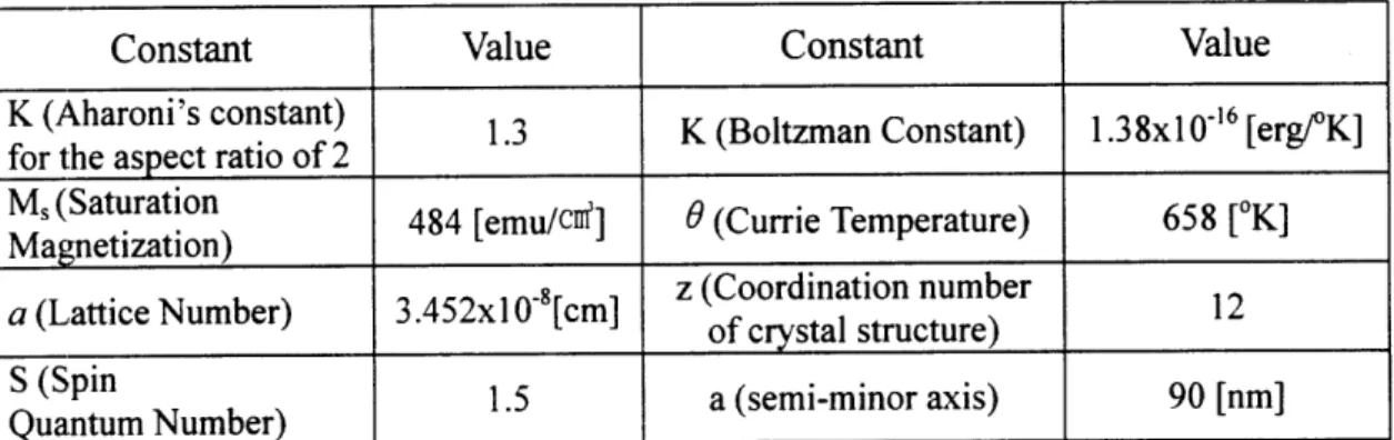
The critical size can be calculated by equating the effects of the two dominant energies in a domain formation, namely the magnetostatic energy and the exchange energy [38]. For a particle smaller than the critical size, exchange interactions become more important than magnetostatic effects and consequently the particles tend to remain uniformly magnetized. However, if a particle is larger than the critical size, the magnetostatic effect is dominant and thus the particle spontaneously breaks up into a number of domains in order to reduce the large magnetostatic energy it would have if it were a single domain. The equation for the critical size of prolate spheroids is given by
aco = qC1/2 /Ms (2.3)
Constant q is a geometry constant that can be found from the graph given by Aharoni for a given aspect ratio of the pillar [38]. Ms is the saturation magnetization and C is the exchange constant. The critical size, ao, is actually the lower bound, as defined by Brown, under which the pillars are always single domain [54]. Using the above equation, we found that a Ni pillar with an aspect ratio of 2 has a critical diameter of 50 nm. Ms of 484 emu/cm3 and C of 7.7x10⁷ were used in the calculation. The exchange constant, C, is actually the least known in the equation and expected to cause errors in the calculations. We used the equation given in [2] as described in Section 2.4 to calculate this constant. Also, in the calculation, we ignored the effect of a slight variation in shape because it's shown that the existence of some variation in geometry does not affect the relevant energies significantly [38]. The diameter of Ni pillars in the test structure is actually larger than the
calculated critical size, leaving possibility that the pillars are not single domains.
2.3.4.2 Experimental Results
The Ni pillars have a cylindrical shape, shown in Figure 2-7 and their average diameter was 90 90 nm
180 nm{
nI1 an the heightl was 180 lll. IU UdeteLrnelll
whether the pillar is a single magnetic domain, we tried to find evidences in MFM images. It's actually difficult to obtain quantitative information from these MFM images, but we Figure 2-7 The dimension of
the pillar concluded that the pillar is a single domain or
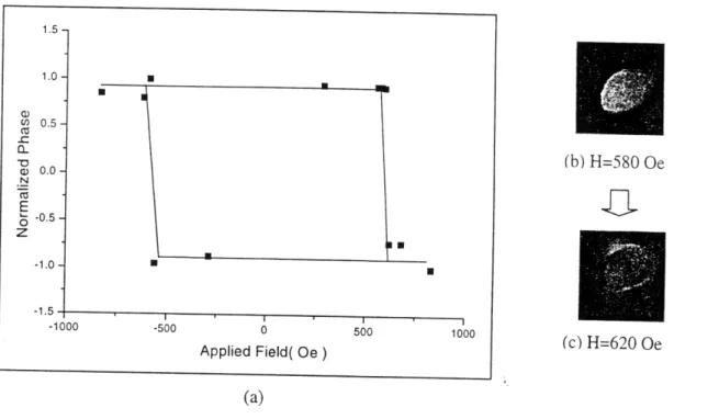
in almost single domain state from the following two facts. First, the MFM image of the pillars resembles the ideal MFM image of the single domain pillar taken with the same orientation of tip and pillar magnetizations. The ideal magnetic image of a pillar has a bright spot at the center and a dark band around it or its reversed pattern. Figure 2-8 (b) and (c) are the experimental MFM images of the pillars, clearly resembling the two ideal images. Secondly, under the changing field, the remanent magnetization state of the pillars is always in one of two equivalent but opposite polarity states. To show this behavior, a plot similar to the hysteresis loop is drawn based on MFM measurements. In Figure 2-8 (a), the horizontal axis represents the applied field and the vertical axis represents a normalized phase obtained from the MFM data. The phase is not an absolute value of the magnetization of the pillar but it can be considered as a value proportional to it. The plot resembles in shape the ideal hysteresis loop of a single domain particle. In the plot, it can be seen that at each corner there exists a sudden switch of magnetization states. In other parts of the plot, there is no change of states regardless of the input field. Figure 2-8 (b) shows the MFM
(b) H=580 Oe
(c) H=620 Oe
(a)
Figure 2-8 (a) Experimental hysteresis loop of a single Ni pillar ( 90 nm x 180 nm )
(b) MFM image at H = 580 Oe (c) MFM image at H = 620 Oe
image of the pillar at an input field of 580 Oe while Figure 2-8 (c) shows the image of the same pillar after the field of 620 Oe is applied. With a small increment of 40 Oe, the magnetic image of the pillar is completely reversed. These behaviors exactly match those of single domain particles.
2.3.5
Results
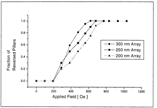
The switching fields of the Ni pillars were measured following the procedure described in Section 2.3.3. The pillars in the 13 x 13 matrix of 300 nm period array were observed under an increasing external field. It is assumed that the effect of the interaction field is very small. Figure 2-9 shows the accumulative fraction of switched pillars at each given external
I o-1.0 -. a, C 0.5--C S0.0-N Cz E S-0.5-z -1.0--1.5 ' I ' I I I -1000 -500 0 500 1000 Applied Field( Oe ) M 1 R