DEMONSTRATING VISIBLY TRANSPARENT SOLAR CELLS AND PHOTODETECTORS by
ANNA JUNGBLUTH
Submitted to the Department of Physics in partial fulfillment of the Requirements for the Degree of
BACHELOR OF SCIENCE
at the
MASSACHUSETTS INSTITUTE OF TECHNOLOGY
June, 2017
@ 2017 ANNA JUNGBLUTH All Rights Reserved
OF T EHNO OGY UJUN
2 22017
LIBRARIES
ARCHIVES
The author hereby grants to MIT permission to reproduce and to distribute publicly paper and electronic copies of this thesis document in whole or in part.
Signature of Author
Dep ment of Physics
( 1t(May 18th, 2017) Certified by _
Professor Vladimir Bulovi6 epartment of Electrical Engineering and Computer Science Thesis Supervisor
Certified by
Professor Janet Conrad Department of Physics Co-Supervisor
Accepted by
The author hereby grants to MIT permission to reproduce and to distribute publicly paper and electronic copies of this thesis document in
Professor Nergis Mavalvala Department of Physics Physics Associate Head
DEMONSTRATING VISIBLY TRANSPARENT SOLAR CELLS AND PHOTODETECTORS by
ANNA JUNGBLUTH
Submitted to the Department of Physics in partial fulfillment of the Requirements for the Degree of
BACHELOR OF SCIENCE
at te OF T HNO OGY
MASSACHUSETTS INSTITUTE OF TECHNOLOGY
JUN
22 2017
June, 2017
LIBRARIES
ARCHIVES
@ 2017 ANNA JUNGBLUTH All Rights Reserved
The author hereby grants to MIT permission to reproduce and to distribute publicly paper and electronic copies of this thesis document in whole or in part.
Signature of
Certified by _
Certified by
-Accepted by
Author
Signature redacted
Dep ment of Physics
A (May 18th, 2017)
Signature redacted
Signatur
Signal
Professor Vladimir Bulovi6 O4 epartment of Electrical Engineering and Computer Science
/9 /Thesis Supervisor
~e
redacted
Professor Janet Conrad Department of Physics
ure
red
acted
Co-SupervisorProfessor Nergis Mavalvala The author hereby grants to MIT permission to Department of Physics
reproduce and to distribute publicly paper and Physics Associate Head
electronic copies of this thesis document in
Demonstrating visibly transparent solar cells
and photodetectors
by
Anna Jungbluth
Submitted to the Department of Physics on May 18th, 2017 in partial fulfillment of the
Requirements for the Degree of Bachelor of Science in Physics
ABSTRACT
The fabrication of inorganic semiconductor devices, such as silicon solar cells and photodetectors, is despite significant research still expensive and energy intensive. Especially for solar cells, high upfront costs are a limiting factor for large-scale fabrication and implementation. Organic semiconductors have attracted increasing attention over the last decade for their optoelectronic properties and potential applications in electronics and photonics. The ease of processing, light weight and low cost of organic semiconductors provides the opportunity for inexpensive, large-scale fabrication. In addition, the mechanical flexibility and bandgap tunability of organic materials enables the fabrication of flexible and semi-transparent organic solar cells and photodetectors that could be installed on any surface and integrated into windows and displays.
This thesis demonstrates visibly transparent solar cells and photodetectors, fabricated using the organic materials tetraphenyldibenzoperiflanthene (DBP) and chloroaluminum phthalocyanine (CIAlPc). We fabricated our devices through spin-coating, thermal evaporation and sputtering and characterized the performance of our devices by measuring the current-voltage behavior, external quantum efficiency and visible transparency. Our devices demonstrate an average visible transparency of around 56%, power conversion efficiencies between 0.53% and 1.36% and specific detectivities on the order of 1011 to 1012 Jones. These values are comparable to results found in literature. The primary goal of this work is to highlight the potential of organic materials for transparent electronics and to provide a detailed overview of the fabrication and characterization techniques needed to advance research in this area.
Acknowledgments
I would like to thank Professor Vladimir Bulovid for the opportunity to join his team of
dedicated researchers in the Organic and Nanostructured Electronics Lab this past semester. I would like to thank ONE Lab research scientist Dr. Anna Osherov and PhD candidate Jonas Xie for their help in getting access to the lab and getting trained on the equipment. I would especially like to thank Dr. Joel Jean for his continuous guidance, support and willingness to help throughout this project. Even though he was more than occupied with his own work, he spent countless hours training me on how to use the equipment, helping me with my measurements and giving me comments on my thesis drafts.
A special thank you goes to my academic and UROP supervisor Professor Janet
Conrad. Janet has given me advice throughout countless academic and personal struggles and has made me feel incredibly supported as a female student in the Physics Department. She will continue to be my role model beyond my time at MIT.
I would also like to thank my family. Without the love and continuous support of my
Table of Contents
T itle P ag e ... 1 A b stra ct ... 2 Acknowledgm ents ... 4 Table of Contents ... 5 1. Introduction ... 8Overview of this thesis ... 11
2. Background ... 12
2.1. Charge Separation ... 12
2.1.1. Inorganic Sem iconductor Devices ... 13
2.1.2. Organic Sem iconductor Devices ... 15
2.2. Device Param eters ... 17
2.2.1. Current-Voltage Behavior ... 17
2.2.2. External Quantum Efficiency ... 21
2.2.3. Noise Equivalent Power and Detectivity ... 23
2.2.4. Transm ittance, Reflectance, Absorbance ... 25
3. M aterials and Experim ental M ethods ... 26
3.1. Device Architecture ... 26
3.2.1. Hole Transport Layers ... 28
3.2.2. Electron Transport Layers ... 29
3.2.3. Electron Donor M aterials ... 29
3.2.4. Electron Acceptor M aterials ... 30
3.2.5. Electrode M aterials ... 31
3.3. Fabrication Techniques ... 33
3.3.1. Substrate Cleaning Procedure ... 33
3.3.2. Spin Coating of PEDOT:PSS ... 34
3.3.3. Evaporation ... 35
3.3.4. Sputtering ... 37
3.4. Characterization Techniques ... 39
3.4.1. Current-Voltage Behavior... 39
3.4.2. External Quantum Efficiency ... 40
3.4.3. Ultraviolet-Visible Spectrophotom etry ... 41
4 . R esu lts ... 4 2 4.1. Device Architecture ... 42
4.2. Current-Voltage Behavior ... 43
4.3. External Quantum Efficiency M easurem ents ... 46
4.4. Absorption and Internal Quantum Efficiency ... 50
4.5. Responsivity, Noise Equivalent Power and Detectivity ... 53
5. Conclusion ... 59
5.2. Recommendations for Future W ork ... 60
Chapter 1: Introduction
Organic semiconductors have attracted increasing attention over the last decade for their optoelectronic properties and potential applications in electronics and photonics [ll. Compared to inorganic semiconductors such as silicon, organic semiconductors are a promising class of materials that offer simple, low-temperature processing, light weight, and low cost [1][2]. This provides the opportunity for inexpensive large-scale fabrication of organic semiconductor devices, such as organic photovoltaics (OPVs) and photodetectors.
Organic photovoltaics have already reached power conversion efficiencies (PCEs) of above 10% [3] and are well on their way to being commercialized as possible low-cost energy sources [4]. Even though this is still lower than the power conversion efficiencies of most inorganic solar cells, organic solar cells have potential applications that inorganic photovoltaics are usually unsuited for. For instance, the mechanical flexibility of organic materials allows the fabrication of OPVs on flexible substrates, such as plastic and paper, as demonstrated by Barr et al. [4]. This would open up opportunities to integrate organic devices on any surface, including clothing and other wearable applications.
Organic semiconductor devices also have the potential to be made semi-transparent if materials are chosen that absorb strongly in the ultraviolet (UV) and near-infrared
(NIR) region [5]. Visibly transparent solar cells, for example, could be easily integrated into buildings on windows and skylights, on automobiles or used as PV chargers on electronic devices [5][6][7]. Previous research into visibly transparent solar cells has focused on many different organic materials to try to maximize both visible transparency and power conversion efficiency; Researchers from the University of California, Los Angeles, for example, achieved PCEs of 4% for solution-processed solar cells with a maximum transparency of 66% at 550 nm
[5],
and MIT researchers have achieved PCEs of 1.7% for thermally evaporated organic solar cells with an average visible transparency (AVT) of around 56% [8]. As a reference, window glass used for automobiles is usually 70% - 80% transmissive and glass used for buildings 55% - 90%transmissive to visible light [8]. According to an analysis performed by Lunt, the theoretical limit of the power conversion efficiency of organic solar cells is 21% with an AVT of 100% [7]. Although it will be difficult to achieve this efficiency in practice, the potential of transparent OPVs is clear. On the large scale, the amount of currently unused space that could be utilized for electricity generation once transparent solar cells become commercially viable could more than compensate for lower efficiencies.
This thesis built on the work of Lunt et al. to fabricate and characterize transparent OPVs. We also included transparent photodetectors in our analysis. Photodetectors that detect near-infrared light are important for many scientific and industrial applications, such as optical communications, remote control, nighttime vision, and chemical and biological sensing, among others [1]. Visibly transparent NIR photodetectors could be integrated into displays and invisible electronic circuits [1]. If these devices are
fabricated onto flexible substrates, transparent NIR photodetectors could help enable technologies such as flexible cell phones and large-area foldable displays [9].
Apart from high materials and manufacturing costs, inorganic semiconductor photodetectors are limited by the inability to tune their spectral response easily
[9].
Organic-based photodetectors, on the other hand, allow easier bandgap tunability due to the variety of inexpensive organic materials available. Polymers with bandgaps as low as
1 eV, the ideal energy range for detecting infrared light, have been used to fabricate
high-performance photodetectors with detectivities greater than 1012 Jones1 [10j, This is comparable to the detectivity of traditional p-n junction photodetectors, which are generally on the order of 1012 to 1013 Jones [111, which highlights the potential of organic semiconductors for the use in photodetectors.
1 The unit Jones is defined as cm - Hz0 5 / W and is a common metric for the performance of a photodetector.
Overview of this thesis
This thesis describes the fabrication of transparent organic solar cells and photodetectors. We focused on chloroaluminum phthalocyanine (ClAlPc) and tetraphenyldibenzoperiflanthene (DBP) as organic electron donor materials, paired with the electron acceptor material C6o and either silver or transparent ITO electrodes.
Chapter 2 provides an overview of the operational principles of solar cells and photodetectors. We discuss the physics of charge separation in inorganic and organic semiconductors and provide an overview of key performance parameters of semiconductor devices. Chapter 3 provides an overview of the materials and device architectures used in this work. In addition, our fabrication and characterization techniques are described in detail. The performance of our devices is characterized in Chapter 4 and the devices are compared based on power conversion efficiency, external quantum efficiency, responsivity, and specific detectivity, among other parameters. Finally, Chapter 5 provides a summary of this work, as well as an overview of the limitations of our results and recommendations for future work.
Chapter 2: Background
Solar cells and photodetectors are semiconductor devices that convert light into current: When incident light is absorbed, electrons are excited, creating electron-hole pairs or excitons. Once the charge pairs are separated, they can be extracted to an external circuit and a current is detected.
Photodetectors are used to detect light of specific wavelength ranges and are frequently run under reverse bias to enhance charge separation and increase responsivity. Solar cells, on the other hand, are used to convert sunlight into useable electricity and are run at the bias that maximizes power output.
2.1. Charge Separation
The following paragraph describes the general operational principles of solar cells and photodetectors based on the process of charge separation in inorganic, p-n junction devices. Since the devices studied in this work were fabricated using organic semiconductors, we will also discuss the process of charge separation in organic semiconductors in more detail.
2.1.1. Inorganic Semiconductor Devices
Devices made of inorganic semiconductors, such as silicon, rely on p-n junctions to create and separate charge pairs. P-type materials are doped with electron acceptors, materials with fewer valence electrons than the bulk, that "accept" electrons and donate electron vacancies, or holes, in return. N-type materials, on the other hand, are doped with electron donors, materials with more valence electrons than the bulk. Doping creates allowed energy states within the bandgap and affects the position of the fermi level with respect to the conduction and valence band of the semiconductor. Compared to the intrinsic case, the presence of impurities shifts the fermi level closer to the valence band for p-type materials, and closer to the conduction band for n-type materials (Figure 1.). Co iduction Hand Electron dft ElIectron diffusio Fermi level Hole diffusion Hfole drift V lence Band
p - type reion n - type
Figure 1. Schematic of a p-n junction. Drift occurs along the electric field. At equilibrium, drift is balanced by diffusion.
When p- and n-type materials are brought together to form a p-n junction, excess electrons diffuse from the n-side to the p-side until the total chemical potential of electrons, the fermi level, is equal on both sides. This causes bending of the conduction and valence band and creates an electric field (Figure 1.). The amount of band bending depends on the doping level; higher doping levels lead to greater band bending and stronger built-in electric fields.
At equilibrium, electron drift along the electric field is balanced by the diffusion of electrons from the n- to the p-side. Outside of equilibrium conditions, when the sample is illuminated or a voltage is applied, either drift or diffusion dominates. Applying a reverse bias to the junction increases the strength of the electric field in the device, which decreases the diffusion current and only the drift current remains. Applying a forward bias, on the other hand, decreases the strength of the electric field, which increases the diffusion current significantly (Figure 2.).
Reverse Bias (Vr) Zero Bias Forward Bias (Vf)
a) Electron drift b) Electron drift
Electron drift
Ec Electron diffusion Electron diffusion Electron diffusion
Ec .E
EF,p q(Vbi -Vr) qVbuilt-in q(Vbi - Vf)
Ev EF~pEFnEFpEn
EF,n E l F evelEF E
Hole diffusion Hole diffusion Hole'diffusion
Hole drift Hole drift Hole drift
Figure 2. Schematic of a p-n junction a) with applied reverse bias, b) without bias, c) with applied forward bias. The dominant charge transport in each case is highlighted.
When the devices are illuminated with above-bandgap light, electrons can be excited from the valence into the conduction band, leaving behind positively charged vacancies or holes. Both the electrons and holes are affected by the electric field and drift away from the junction. The charges then need to collected at the electrodes for the
light-induced current to be extracted.
2.1.2. Organic Semiconductor Devices
One of the main differences between the operational principles of inorganic and organic semiconductor devices is the process of charge separation. Compared to the conduction and valence band structure of inorganic semiconductors, the ground and excited state in an organic semiconductor are described by the highest occupied molecular orbit (HOMO) and lowest unoccupied molecular orbital (LUMO) respectively [12]. The energy difference between the HOMO and LUMO is generally well defined for different materials and can be thought of as an equivalent to the optical bandgap of organic semiconductors [131. The absorption of a photon can excite an electron to create a quasi-particle called an exciton (Figure 3.a)). Excitons are bound states between electrons and holes and are created through mutual coulomb interactions. In order to extract a current, excitons need to be separated into unbound charge carriers before they recombine. In organic photovoltaics, separation of an exciton can be achieved through effective fields at the interface of two materials with different conduction band energy levels: An exciton created in the absorber material can be separated if the electron "falls"
from the conduction band of the absorber to the lower energy conduction band of the acceptor material, as shown in Figures 3.b)-c) 1121. Applying a reverse bias to the junction causes the energy levels of the electron donor material to be lifted up compared to the energy levels of the acceptor material. This creates a higher driving force to
separate the exciton into charge pairs.
Once the charges are separated, they can easily be extracted through the application of an electric field. In addition, electron and hole transport layers that have high electron or hole affinities and block the other carrier type can help extract charges more easily
(Figure 3.d)).
Organic devices either consist of a single layer of active material (Schottky devices), separate layers of donor and acceptor material or a bulk heterojunction with the donor and acceptor material blended together
1121.
The devices used throughout this study consisted of discrete layers of donor and acceptor materials; the exact architecture and materials used will be discussed in more detail in Chapter 3.a) b) c) AELUMo d) as driving I I force LUMO _ Photon I I HOMO Donor Acceptor
Exciton Generation Exciton Diffusion Exciton Dissociation Charge Collection
Figure 3. Schematic of the processes required for charge separation in organic
2.2. Device Parameters
The following paragraphs give an overview of key parameters determined to evaluate the performance of our devices as solar cells and photodetectors. We measured the current-voltage behavior, external quantum efficiency and absorption of our devices to calculate the efficiency, spectral response, responsivity, noise equivalent power and specific detectivity.
2.2.1. Current-Voltage Behavior
The current-voltage (J-V) behavior of a semiconductor device can be used to determine the power conversion efficiency and the maximum power that can be extracted. Figure 4. shows the schematic of a current-voltage curve in the dark and under illumination. The current at zero applied voltage is called the short circuit current (Jsc). The open-circuit voltage (Voc) is the voltage required to balance drift and diffusion of charges and achieve a net zero current in the device. The shape of the current-voltage curve in the dark can be described by the ideal diode equation, given as
qV
I = IO[exp( )- 1] Equation 1.
where I is the current, Io is the "dark saturation current" or leakage current in the absence of illumination, V is the applied voltage across the device and n is the ideality factor. For ideal diodes, the ideality factor is equal to one, while for non-ideal diodes the ideality factor is a number between one and two.
The efficiency of a diode can be determined from the diode's current-voltage behavior under illumination according to
VOCJscFF
Equation 2.
Pin
where V0c is the open-circuit voltage, Jsc is the short circuit current, FF in the fill factor and Pin is the power of the incident light,. The fill factor is a unit-less quantity that relates the maximum power that can be extracted from the device to the short-circuit current and the open-circuit voltage as
FF = Pmax Equation 3.
The higher the fill factor, the more power can be extracted from the device and the better the device functions as a solar cell. [14]
Without Illumination .ilder' Illuninatioii 6 '-4 Open-Circu Voltage (Vc U Pmax it )o *Voltage -I Short Circuit Current (Jsc)
Figure 4. Schematic of a current-voltage curve in the dark and under illumination.
The shape of the current-voltage curve also reveals useful information about resistances present in the device. Figures 5.a)-b) show schematics of current-voltage curves with influences from series and shunt resistances. The series resistance arises from internal resistances present in the device, such as the contact resistance between the active layer and the electrodes [15][161. The series resistance does not influence the device at open-circuit, since the current through the device and consequently through the series resistance is zero [16]. The series resistance does, however, decrease the short circuit current and the fill factor. An estimate of the series resistance can generally be obtained
resistances generally arise due to manufacturing defects [17]. Shunt resistances can be treated as parallel resistances in a device; ideal devices therefore have infinitely high shunt resistance. A low shunt resistance provides an alternate current path through the device and therefore results in power loss [17]. Compared to the series resistance, the shunt resistance does not influence the short circuit current but decreases the open-circuit voltage. An estimate for the shunt resistance can be determined from the slope of the current-voltage curve near short circuit [17].
Figure 5. Schematic of a current-voltage curve with a) high series resistance,
a) 0 Voltage High Series Resistance Ideal Diode b) - Voltage Low Shunt Resistance Ideal Diode
2.2.2. External Quantum Efficiency
External quantum efficiency (EQE) measurements allow us to determine the photoresponse of devices, both solar cells and photodetectors, as a function of wavelength. More specifically, EQE measurements reveal the photon-to-electron conversion efficiency, which is the ratio of the number of charge carriers collected to the number of photons incident on the device. The external quantum efficiency can be calculated using
'ph hv
EQE = -- 100% Equation 4.
q PO
where Iph is the measured photocurrent, q is the elementary charge, h is Planck's
constant, v is the frequency of the incident light and Po is the incident optical power at that wavelength [131. The EQE response of an ideal solar cell is shown in Figure 6.a). If all photons in the energy range above the bandgap are absorbed and converted to charges, the external quantum efficiency reaches unity. However, generally, the EQE is reduced through reflection of light at the surface and recombination within the device. Below the bandgap, no light is absorbed and the EQE is zero [181.
Similar to the external quantum efficiency, the spectral response (SR), or responsivity (R), relate the number of charges to the incident light power [19]. The spectral response and the responsivity can be calculated using
Equation 5. SR = EQE = ph100% hv Po ph SR PO 100% Equation 6.
Both the spectral response and the responsivity are important metrics to characterize photodetectors. Figure 6.b). shows the responsivity of an ideal solar cell. Similarly to the
EQE spectrum of an ideal solar cell, no light is absorbed below the bandgap. However,
compared to the EQE, the responsivity decreases at low wavelengths due to the increasing energy per photon [20].
l(1(;Ii EQIV a)
1-Reduced EQE No light is absorbed
ohdue to I below the reflection and baldgae recombination Wavelength b) Reduced Responsivity Wavelength Figure 6. a) External b) spectral
quantum efficiency of an ideal and a non-ideal device, response of an ideal and a non-ideal device.
2.2.3. Noise Equivalent Power and Detectivity
The sensitivity is one of the most important characteristics of a photodetector. The noise equivalent power (NEP) is a commonly used metric to describe a photodetector's sensitivity. The noise equivalent power is defined as the incident power needed to achieve a unity signal-to-noise ratio in a 1 Hz output bandwidth and is therefore a measure of the weakest optical signal that can be detected [211. The units of the NEP are watts per square root of hertz [22]. The NEP can be calculated by using
NEP = - Equation 7.
R
where In is the root-mean-squared (RMS) noise current and R is the responsivity, determined through EQE measurements [13].
The RMS noise current In depends on the dominant noise mechanism in the diode.
Without applied bias, the dominant noise is assumed to be Johnson-Nyquist noise, or
thermal noise, defined as
IJN = 4kbAf Equation 8.
where kb is Boltzmann's constant, Af is the bandwidth and RD is the differential
resistance of the diode, measured at zero bias [13]. With applied bias, shot noise is assumed to be the dominant noise. Shot or Poisson noise originates from the discrete nature of charges or photons and is given by
Equation 9. shot = 2qI.,k-Af
where q is the elementary charge and Idark is the dark current of the diode with applied
bias [13]. The total noise current under bias can then be calculated as
In = IjN +I Equation 10.
Once the noise equivalent power is determined, the detectivity (D) can simply be calculated as the inverse of the NEP. Normalization of the detectivity with respect to the device area yields the specific detectivity (D*) according to:
Equation 11. AD
NEP
where AD is the active area of the device and Af is again the bandwidth over which the
2.2.4. Transmittance, Reflectance, Absorbance
We also conducted measurements of the transmittance and reflectance at normal incidence using Ultraviolet-Visible Spectrophotometry (UV-Vis) to determine the absorption spectra of our devices. To quantify reflectance, the intensity of the light reflected off of the sample (I) to the intensity of the incident light onto the sample (Jo) is measured. The reflectance is then calculated as the ratio I/Io. The transmittance is similarly measured by comparing the intensity of light transmitted through the sample to the intensity of incident light. The absorbance of our devices can then be calculated as the logarithm of the transmitted light, using
% T
A = -log( ) Equation 12.
100%
We were primarily interested in the percent of absorbed light, which we calculated using
Chapter 3: Fabrication and Characterization Techniques
3.1. Device Architecture
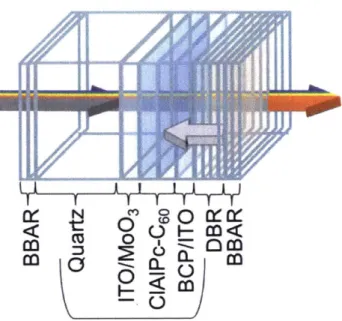
The device architecture used throughout this study was based off of the devices fabricated by Lunt et al. (Figure 7.) [8]. Lunt et al. use molybdenum oxide (MoO3) as a hole transport layer, chloroaluminum phthalocyanine (ClAlPc) as the organic donor, and Co as the organic acceptor material. Lunt et al. also include a distributed Bragg reflector (DBR) as a near-infrared mirror at the back of the device, as well as broad band antireflection (BBAR) coatings on both sides to minimize reflection
18].
To simplify our device architecture, given the limited time available to work on this project, we decided to leave out the DBR and BBAR coatings and accepted the resulting decrease in efficiency.Table 1. summarizes the device architecture, materials and thicknesses used for this study. A schematic of the ITO patterned substrates used, purchased from TFD, is shown in Figure 8. For most of our devices, PEDOT:PSS instead of MoO3 was used as a hole transport layer, for reasons that will be explained in more detail in Chapter 4. Apart from ClAlPc, we also included tetraphenyldibenzoperiflanthene (DBP) as a potential electron donor material in our analysis. We initially fabricated all of our devices with non-transparent silver electrodes as controls and later moved to sputtering transparent ITO electrodes.
-I_
6'
0aC
F
I
I
I
3 < oFigure 7. Original device architecture as demonstrated by Lunt et al.
Figure 8. Schematic of the
ITO-patterned glass substrates used
Table 1. Summary of device architectures, materials and thicknesses used.
Material
Substrate ElectrodeThickness
0.68 mm 150 nmHole Transport Layer Electron Donor Material Electron Acceptor Material Electron Transport Layer
MoO3, PEDOT:PSS ClAlPc, DBP C60 BCP 20 nm, 50 nm (respectively) 25 nm 30 nm 7.5 nm 100 nm, 150 nm (respectively)
in
SO I I 00 0.495 in Glass ITOElectrode Ag, ITO
i 2
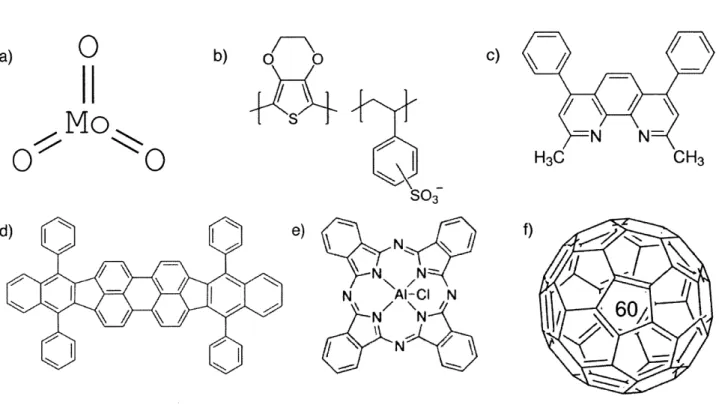
3.2. Materials
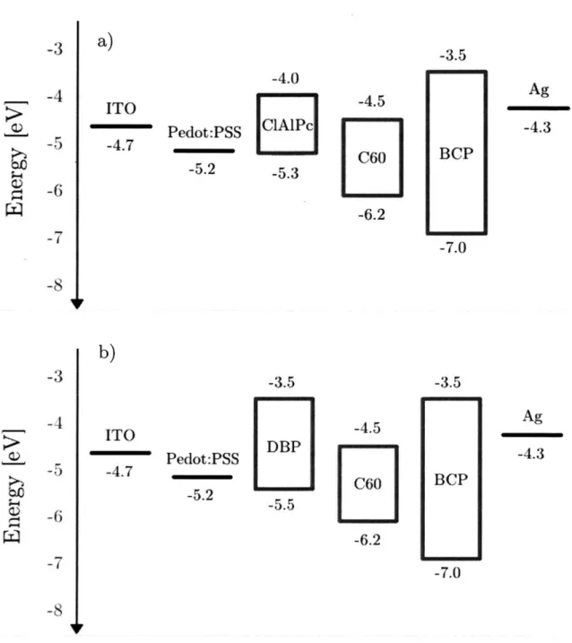
The following paragraphs provide a brief overview over the materials used throughout this work. Figures 9.a)-f) show the 2D structure of the materials and Figures 10.a)-b) show the energy diagrams for the ClAlPc and DBP devices fabricated with silver electrodes.
3.2.1. Hole Transport Layers
Molybdenum trioxide
One of the hole transport layer materials used was molybdenum(VI) oxide (MoO3), purchased from Alfa Aesar (Puratronic, 99.9995% purity, Product No. 12930). MoO3 has a molecular weight of 143.94 g/mol and MoO3 powder sublimates at 1155 C [23J. The
HOMO and LUMO levels of MoO3 are -9 eV and -5.8 eV respectively [24] and the structure of MoO3 is shown in Figure 9.a). We deposited 200 A thick MoO3 films
through thermal evaporation.
PEDOT:PSS
Poly(3,4-ethylenedioxythiophene):poly(4-styrenesulfonate) or PEDOT:PSS is a commonly used hole transport layer [251. The material was purchased from Heraeus (Clevious, P VP Al 4083) and the structure of PEDOT:PSS is shown in Figure 9.b).
The energy level of PEDOT:PSS is reported as -5.2 eV [24]. We used spin coating to deposit 500
A
thick layers of PEDOT:PSS onto our substrates.3.2.2. Electron Transport Layers
BCP
We used bathocuproine, or BCP for short, as an electron transport layer for our devices. The material was purchased from Lumtec (Product No. LT-E304) and was used without further purification. BCP has the molecular formula C26H2oN2 and a molecular weight of
360.45 g/mol [26]. The HOMO and LUMO levels of BCP are -7 eV and -3.5 eV
respectively [26]. The 2D structure of BCP is shown in Figure 9.c).
3.2.3. Electron Donor Materials
CiAlPc
We used chloroaluminum phthalocyanine (ClAlPc) as one of two electron donor materials for our organic devices. CIAlPc has been used in a number of studies as an electron donor material, such as
18][27][28].
The material was purchased from TCI (Product No. C1167, with >98.0% purity) and was used without further purification. CIAlPc has the molecular formula C32H16A1C1N8 and a molecular weight of 574.97 g/mol[291. The HOMO and LUMO levels of CIAlPc are -5.3 eV and -4 eV respectively [30].
DBP
The other electron donor material used was tetraphenyldibenzoperiflanthene (DBP). The material was purchased from Lumtec (Product No. LT-N4003) and used without further purification. DBP has the molecular formula C64H36 and a molecular weight of
804.97 g/mol [31]. The HOMO and LUMO levels of DBP are reported as -5.5 eV and -3.5 eV respectively [31]. The structure of DBP is shown in Figure 9.e). DBP has
previously been used as an active material for organic solar cells, for instance, to fabricate the thinnest and lightest solar cell [32][331.
3.2.4. Electron Acceptor Materials
Fullerence-C60
Buckminsterfullerene is a spherical fullerene molecule with molecular formula C60
(Figure 9.f)). The material was purchased from Lumtec (Product No. LT-S903) and was purified once by thermal gradient sublimation before use. C6o has a molecular weight of
720.64 g/mol [34]. The HOMO and LUMO levels of C6o are reported as -6.2 eV and -4.5 eV respectively [34]. Because of its high electron affinity, C6o has often been used as an electron acceptor in organic devices [8][35][4].
3.2.5. Electrode Materials
Silver
We evaporated 1000A thick layers of silver as electrode materials for the control devices. The work function of silver was reported as -4.3 eV [361.
Indium tin oxide
A 1500A thick indium tin oxide (ITO) layer was sputtered onto our samples as a
transparent electrode. The work function of ITO was found to be -4.7 eV
124].
a)
0
b) oMo
0<
0
d) 0Is
S03 e) rN N 'Al-Cl N N N NFigure 9. Schematic of the 2D structure of the materials used: a) MoO3, b) PEDOT:PSS,
c) BCP, d) DBP, e) ClAlPc, f) C60
C)
-N N~
H3C CH3
Pedot:PSS -5.2 -3 -4
-5
-6 -7 -8 -3 -4 -5 -6 -7 -8 -4.0 -4.5 ICIAlPc I1C601
-5.3L i
-6.2 -3.5 -4.5 DBP C60 -5.5 -6.2Figure 10. Band diagram of devices with ITO and silver electrodes and a) ClAlPc, b) DBP as an electron donor material
a)
ITO -4.7 -3.5 Ag -4.3 BCP -7.0 Pedot:PSS -5.2 b) ITO -4.7 -3.5 Ag -4.3 BCP -7.03.3. Fabrication Techniques
3.3.1. Substrate Cleaning Procedure
Throughout this work, a standard cleaning procedure was used to clean substrates before solution processing and thermal evaporation. The standard cleaning procedure involved multiple steps of cleaning, rinsing, sonicating and boiling the substrates in different solvents to remove both organic and inorganic compounds. The exact procedure is outlined in more detail in the following paragraph.
The first step of the cleaning procedure involved scrubbing each substrate with a Q-tip and soap water (1 part micro-90 (Cole-Parmer) and 400 parts deionized water) to manually remove any larger dust particles from the surface. The substrates were then rinsed with deionized water and placed in a substrate holder inside a beaker filled with soap water. The beaker was placed inside the water bath of an ultrasonic cleaner (VWR Scientific Products, AQUASONIC, Model 50T) and the substrates were sonicated for five minutes. Ultrasonic cleaning is an important part of the cleaning procedure that helps remove contaminants adhered to the surface of substrates. The ultrasonic cleaner works on the principle of using ultrasound waves (usually from 20 - 400 kHz) to agitate a liquid. The alternating pressure inside the liquid causes micron-sized bubbles to form. When these bubbles implode, strong forces and high temperatures and pressures act on the surface of the substrates to remove contaminants without damaging the substrates
[37]. After sonicating the substrates in soap water for five minutes, the substrates were
sonicated in deionized water and acetone for another five minutes each. At the same time, two beakers filled with isopropanol were heated to boiling on a hot plate. After sonicating, the substrates were placed in the beakers filled with boiling isopropanol for five minutes each. The last step of the cleaning procedure involved plasma cleaning the substrates for two minutes. The substrates were placed in a remodeled microwave (Plasmatic Systems, Inc.) and the chamber was slowly put under vacuum. Oxygen was used to create an energetic plasma. The energetic plasma emits UV light when atoms and molecules relax from their excited state, and this UV radiation is effective in breaking organic bonds of surface contaminants. After plasma cleaning, the substrates were placed in cleaned fluoroware and safely stored away.
3.3.2. Spin Coating of PEDOT:PSS
The first part of the fabrication process involved spin coating a layer of PEDOT:PSS as the hole transport layer. Spin coating is a process commonly used to deposit thin films of materials onto substrates. A small amount of material is placed in the middle of the substrate, which is then rotated at high speeds to uniformly distribute material on the surface.
The substrates were plasma cleaned for 5 minutes and then placed on the holder of the spin coater (Headway Research, Inc., Model PWM32). We deposited 45 microliter of
RPM for 50 s with a ramp-up time of 1 s. The resulting thickness was approximately 50 nm. After spin coating, the substrates were placed on a hot plate at 120 C for 15 mins to evaporate the residual solvent. The substrates were then immediately stored in a nitrogen-filled glovebox to avoid degradation.
3.3.3. Thermal Evaporation
The metals and organic materials used in this work were deposited through thermal evaporation. Figure 11. shows a schematic and a photograph of the thermal evaporator system used throughout this work. The materials were loaded in metal crucibles and screwed in place inside the evaporator. The evaporator was then pumped down to vacuum over night and a base pressure of 10-6 Torr was kept throughout the evaporation process. The substrates were secured inside a substrate holder and placed on a rotating metal stage above the crucibles. The rotation was required to assure a more uniform film deposition. An DC current was delivered to the metal crucibles, which caused the metal to heat up and the materials to sublime. Some of the evaporated source material then condensed on the substrates to form a thin film. The rate of deposition of the materials, which was usually kept at around iA/s, was directly controlled by the amount of current supplied to the crucibles and measured through a quartz crystal monitor. The quartz crystal monitor also measured the thickness of the deposited material. However, since the monitor was not in the exact same location as the substrates, the thickness reading
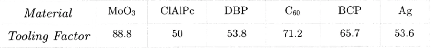
was generally not the same as the actual thickness of the films on the substrates. In order to correct for the difference, a "tooling factor" had to be determined beforehand.
Before we started fabricating full devices, we therefore deposited thin films of materials on silicon substrates and determined the thickness through fitting of optical models. The relationship between the actual and determined thickness let us determine the actual tooling factor according to [38]
ToolingapproximateThicknessActual
Thickn essmeasured Equation 14.
The tooling factor was location specific and had to be remeasured if the location of the crucible for a certain material was changed. Table 2. summarizes the determined tooling factors for the materials used throughout this work.
Table 2. Tooling factors of materials deposited through
Material MoO3 ClAlPc DBP
Tooling Factor 88.8 50 53.8 thermal C60 71.2 evaporation. BCP 65.7 Ag 53.6
substrate rotation vacuum chamber thickness monitor -samples crucibles V power supply
Figure 11. Schematic and photograph of the thermal evaporator system used [131.
3.3.4 Sputtering
Metal oxides, such as ITO, and other materials with high melting points can generally not be deposited through thermal evaporation but have to be deposited through a process called sputtering instead. Rather than evaporating the source material, high energy ions are bombarded onto the surface of the target material to eject particles that can then condense onto the surface of the substrates. Figure 12. shows a schematic of the sputtering process and a photograph of the ONE Lab sputtering system used throughout this study.
Source material was placed inside the sputtering chamber and the chamber was pumped down to <105 Torr. The substrates were then loaded onto a metal stage above the target material. The high energy ions used to bombard the source material were created by ionizing incoming argon gas and creating an argon plasma. The argon ions were then accelerated onto the target and source material was ejected. The ejected particles traversed through the chamber and condensed onto the surface of the substrates. The rate of deposition was controlled by monitoring the gas pressure inside the chamber and controlling the power used to ionize the argon gas [13].
Ar ions target
.grounded shield RF electrode
ring magnet
water cooling Argon gas to RF
power-supply
3.4. Characterization Techniques
In order to avoid degradation of the devices, most characterization measurements were conducted in a glovebox filled with nitrogen. The devices were placed in a custom-built test fixture and secured in the different testing equipment. The following paragraphs provide information about the equipment and machines used to conduct our measurements.
3.4.1. Current-Voltage Behavior
As described in detail in Chapter 2, determination of the current-voltage behavior is one of the main tools to characterize the performance of devices: Measuring the current-voltage behavior allowed us to determine the power conversion efficiency and fill factor of our devices, among other characteristics.
The J-V measurements were performed using a Keithley 6487 picoammeter, with 100
10 mW cm 2 simulated solar illumination provided by a 150 W Newport 96000 xenon
arc-lamp equipped with an AM1.5G filter and a diffuser lens [391. We consistently performed a forward and backward scan from -IV to +1V with a step size of 0.05V. Measurements were performed under illumination and in the dark.
3.4.2. External Quantum Efficiency
A schematic of the experimental setup used to measure the external quantum efficiency
is shown in Figure 13. Monochromatic light from a 1000 W xenon arc lamp (Newport Model 66921) was focused through an optical chopper into an Acton Spectrapro 300i monochromator and then through an optical fiber into the glovebox. The incident optical power (Po) of the light source was measured by focussing the light from the optical fiber onto a calibrated devices (Newport 818-UV) and the spectrum was recorded. Afterwards, the devices are secured in the test fixture and placed straight under the optical fiber. The photocurrent was measured through a lock-in amplifier (Stanford Research Systems Model 830) [13]. We consistently scanned from 300 nm to
1100 nm, with a step size of 4 nm. We performed EQE measurements at zero bias, as
well under reverse biases of up to -4V.
Voltage Source
Nitrogen Glove Box
Lamp Lens Chopper Fiber Sample
Mlonochromator +Lock-in Amplifier
~ I
.J U L
-rU J PC
PC
Figure 13. Schematic of the external quantum efficiency setup used throughout this work [13].
3.4.3. Ultraviolet-Visible Spectrophotometry
In order to measure the reflectance and transmittance of our devices, we performed Ultraviolet-Visible Spectrophotometry using a Varian Cary 5000, ultraviolet, visible light and near-infrared spectrophotometer. Before measuring our samples, multiple background scans were performed. For the reflectance measurements, an aluminum mirror with known reflectance spectrum was placed inside the UV-Vis and a baseline scan was performed, capturing almost all of the incident light. Afterwards, a zero scan was performed with an empty sample holder. Without reflection of the incident light, the detector can capture electrical noise and background light from outside. For measuring transmittance, the baseline scan was performed with an empty sample holder so that all of the incident light went directly into the detector. The zero scan was performed by blocking the incident light with a black piece of card board. Afterwards, the samples were loaded in the detector and both reflectance and transmittance scans were performed. We consistently measured from 300 nm to 1200 nm with a step size of 2 nm.
Chapter 4: Results
4.1. Device Architecture
As described in Chapter 3, our device architecture was originally based off of the device architecture demonstrated by Lunt et al. [13]. We started by fabricating devices with MoO3/ClAlPc/C6o/BCP and used silver for the second electrode. Evaporating silver is
generally easier and more predictable than sputtering ITO. Since particles are bombarded onto the substrates, the sputtering process can be quite harsh. We therefore decided to fabricate control devices with silver first to make sure none of the other materials were degraded.
The first round of devices we fabricated were all shorted. We hypothesized that the ClAlPc, which had been purchased and opened in 2015, had degraded. We purchased a new bottle of the material from TCI, with 98.0% purity, and fabricated a new round of devices without further purification. The devices, however, were all shorted again. We came up with two possible explanations: either our newly purchased chloroaluminum was not pure enough and would need to be purified even more, or the molybdenum trioxide we used was degraded. We therefore decided to fabricate a next set of devices, with either MoO3 or PEDOT:PSS as a hole transport layer, and DBP instead of CIAlPc
molybdenum trioxide worked and concluded that the problem stemmed from MoO3. We therefore decided to move forward with using PEDOT:PSS instead of MoO3.
After confirming that none of the other materials were degraded, we planned out the four device architectures we wanted to focus on during this study (Table 3.). The following paragraphs summarize the results of our characterization measurements.
Table 3. Device architectures studied throughout this work.
Device Architecture
Electrode
Hole Transport Layer
Electron Donor Material
Electron Acceptor Material
Electron Transport Layer
Electrode
ITO ITO ITO
PEDOT:PSS PEDOT:PS PEDOT:PS
S S fl-P -BCP Ag BCP ITO BCP Ag ITO PEDOT:P SS CIAlPc BCP ITO
4.2. Current - Voltage Behavior
Figure 14.a) shows the current-voltage curves measured under illumination, Figure 14.b) shows a semi log plot of the I-V behavior in the dark and Table 4. summarizes the determined short circuit current, open-circuit voltage, fill factor and efficiency for DBP and ClAlPc with either silver or ITO electrodes. Similar devices presented in literature show comparable results: Our DBP control devices show a similar open-circuit voltage,
but lower short circuit current than organic solar cells presented by Fujishima et al., who used DBP and C6o as active materials and aluminum as a cathode, and whose
devices reached a PCE of 3.6% [35]. Compared to the work presented by Lunt et al., our ClAlPc controls exhibit a lower short circuit current, open-circuit voltage and efficiency. Our transparent ClAlPc devices, however, exhibit a similar short circuit current and open-circuit voltage with the same efficiency [8].
Smaller bandgaps generally lead to a higher short circuit current and a lower open-circuit voltage [40]; ClAlPc, which has a smaller bandgap than DBP (Figure 10.), does indeed exhibit a larger short circuit current and smaller open-circuit voltage in the control case.
For both the ClAlPc and DBP devices, switching from silver to ITO as an electrode material decreases the short circuit current. This is due to the fact that ITO reflects less light than silver back into the active area, which decreasing the overall light absorption
[8]. Compared to the ClAlPc devices, our DBP devices display a smaller drop in the short circuit current and the efficiency when moving from a silver to an ITO electrode. The open-circuit voltage, on the other hand, was not affected by this change and stayed constant in both cases.
Compared to an ideal current-voltage curve (see Chapter 2), the shape of the curves of our devices suggests low shunt resisances. Especially the fairly large slope in the reverse bias region of both ClAlPc devices suggests the presence of a low shunt resistance. Low shunt resistances lead to power loss by providing alternate current paths for light-generated current and typically arise from manufacturing defects [17]. Similar slopes can
be found in the ClAlPc devices fabricated by Lunt et al. [8]. Since our DBP devices do not exhibit the same high slope in the reverse bias region, despite having been fabricated the exact same way as the ClAlPc devices, we are hypothesizing that these defects arise from interactions of CIAlPc with the other layers, e.g. poor energy level alignment.
0 C9' 4 4 Z U -1 -2 -3 -4 -5 -1.00 -0.75 -0.50 -0.25 0.00 0.25 0.50 0.75 Voltage IV] 1.0( 10 -DBP /Ag - DBP /ITO 100 - CIUPc /Ag -- CLAJPc / ITO 10-1 10-2. 10-10-5 b) 10-6 -1.00 -0.75 -0.50 -0.25 0.00 0.25 0.50 0.75 1.00 Voltage [V
Figure 14. a) Current density vs. voltage measured for our devices under illumination,
b) Semilog plot of the current-voltage behavior in the dark.
- DBP /Ag
- DBP /ITO
-- CIAlPc / Ag
- CIAPc /ITO
Table 4. Summary of short circuit currents, open-circuit voltages, fill factors and efficiencies determined for our devices.
Structure
Jsc[A/cm
2] Voc /V] Fill Factor EfficiencyDBP
/
Ag 3.40 +/- 0.02 0.9 +- 0.0 0.58 /- 0.02 1.807-
0.06 %DBP
/
ITO
2.86 +/- 0.02 0.877-
0.01 0.55 +/- 0.01 1.367-
0.06 %CiA
lPc/
Ag 3.88 / 0.01 0.68 / 0.01 0.43 / 0.01 1.14 +/- 0.06 %ClAlPc ITO 1.7 +/- 0.04 0.68 +/- 0.02 0.46 +/- 0.01 0.53 +/- 0.02 %
4.3. External quantum efficiency measurements
We conducted external quantum efficiency measurements with and without bias on all of our devices. We scanned over a wavelength range from 300 - 1100 nm with a step size of
4 nm. Figure 15. shows the EQE spectrum for the devices comparing the samples with silver and ITO electrodes with no bias applied. As can be seen on the graphs, the EQE is significantly higher for the samples with a silver electrode. This can again be attributed to the fact that silver reflects transmitted light back into the cell, causing more light absorption and a higher photocurrent. The EQE spectra also confirm the larger bandgap of DBP; DBP starts to absorb at around 650 nm, while ClAlPc starts to absorb at 850 nm. ClAlPc is therefore a more suitable material for applications that require light absorption in the infrared region of the spectrum. Both materials absorb decently well in the UV. The EQE of ClAlPc, however, seems to drop quicker when moving to shorter wavelengths; at 300 nm, the EQE of DBP with silver electrodes is still
at 15%, while the EQE of CIAlPc with silver electrodes drops to around 7%. This difference is equally apparent for the samples fabricated with ITO electrodes.
Compared to the ClAlPc devices, DBP absorbs strongly from 500 - 650 nm, with a local
maximum around 615 nm and a minimum at around 450 nm. The ClAlPc devices absorb more than the DBP devices in the blue region, from 400 - 500 nm, and then
again in the wavelength range from 600 - 800 nm, with a minimum at around 550 nm
(Figure 15.). 30-a) 25- --- DBP /ITO 20. 15- 10-300 400 500 60O 700 800 900 1000 1100 Wavelength ini 30 - b)__ iP 2C-AIPc / >125- S20-15 10-300 40O 500 60O 700 800 90 1000 1100 Wavelength [nm]
Figure 15.a) External quantum efficiency of DBP samples with either silver or ITO electrode,
Inefficient exciton diffusion and charge separation are often the limiting factors for achieving higher efficiency devices. Applying a reverse bias can help separate excitons more easily. Especially for photodetectors, applying a reverse bias is an important tool to increase the responsivity. We therefore performed EQE measurements and applied reverse biases of up to -4V. Most of our samples were not able to sustain negative voltages of -4V; current started to leak through the devices, causing random spikes in the EQE spectra. We therefore decided to leave out too high reverse biases from our analysis.
Figures 16 a)-d). show the EQE spectra of all four types of devices under varying reverse biases. As expected, the photocurrent and hence the external quantum efficiency increases when a reverse bias is applied. After reverse biasing, we repeated the measurements without an applied bias to make sure our devices did not degrade over time. We found that the zero bias measurements were mostly reproducible. The ClAlPc and silver sample, however, seemed to have degraded. When we first conducted measurements on this device, the maximum EQE was around 30% at 450 nm (Figure
15.). Remeasuring revealed that the maximum EQE had dropped to around 15% at the
same wavelength (Figure 15.b)). We tested other pixels on the device, which also revealed degradation.
35- 30- 25- 20-15, 10-51 F Z 3) 0 0, U CIAlPc / Ag . L_ _-- - -1. - -2. -- 3. c) 4iO 0 0 v 0 V 0 v -6V -- 0.5 V -1.0 V -2.0 V a) y -- 4 35 30-25 20 15 10- 5- 0-Soo 550 600 650 700 Wavelength [rmn] b) DBP / ITO, 35. 30- 25- 20*15 - 10.-5. 0 4 d) 400 Soo 550 600 Wavelength [nm] CiAlPc/ ITOI 450 500 550 Wavelength [mn]
Figure 16. External quantum efficiency curves with zero bias and varying reverse biases applied for a) DBP with silver, b) DBP with ITO, c) CIAlPc with silver, d) ClAlPc with ITO electrode.
)0 450 - ov -0.5 v -1.0 V -1-3.0 V 1400 45O 500 550 60 65O 70 Wavelength [nm] 3 30 -25 - 20- 15-10. 650 700 -- 1.0V - .0 V 400 600 650 700 ZZ ----
-4.4 Absorption and Internal Quantum Efficiency
We also conducted UV-Vis measurements to determine reflection, transmission and absorption of light through the devices with ITO electrodes (Figure 18.). Figures
17.a)-b) show photographs of the transparent DBP and ClAlPc devices. In the visible region,
our DBP devices have an average visible transmission (AVT) of 56% with a peak transmission of 60% at around 530 nm. The transparent CIA1Pc devices show an average visible transmission of 57% with a peak transmission of around 73% at 560 nm. The determined peaks in transmission match the minima in the EQE signal. Lunt et al. ClAlPc devices of similar architecture demonstrated an AVT of 65
+/-
3% [8].Even though the EQE signal of both transparent ITO samples decreased to almost zero below the bandgap, the absorption curves show non-zero absorption in this region. High-quality ITO absorbs strongly in the IR because of free-carrier processes. The high density of free carriers that produce high conductivity also increases the light absorption
by allowing intraband excitation
of carriers into higher states.
onone
a)
Figure 17.a) Transparent DBP and ClAlPc devices on a piece of paper, b) DBP device c) CIAlPc device held up in front of the ONE Lab sign.
DBP
/ITO
100a)
8060 -60-- Reflection -- Transmission - Absorption 40- 20-300 400 500 600 700 800 900 1000 1100 Wavelength [nm]CIA1Pc
/
ITO
100b)
80- 60--- Reflection -- Transmission -- Absorption 40- 20-300 400 500 600 700 800 900 1000 1100 Wavelength[nm]
Figure 18. Reflection, transmission and absorption curves determined for a) transparent DBP devices, b) transparent ClAlPc devices.
In order to quantify how much absorbed light is actually converted to photocurrent, we also looked at the internal quantum efficiency of our transparent devices (Figure 19). The internal quantum efficiency gives the ratio of extracted, photo-generated charges to the number of charges incident on and absorbed by the device. The IQE was calculated
using
EQE _EQE
IQE = A 1RT Equation 15.
A 1- R- T
While this equation is in principle correct, it does not take optical interference and parasitic absorption in non-active layers, such as PEDOT:PSS and ITO, into account [411. Parasitic absorption can, for example, be determined through transfer matrix models, which we were not able to perform in the time allocated for this project. Figure
19. does therefore not represent the actual IQE, but can still be used as a guideline to
50 40- 30- 20-10. S+--300 Figure 19. IQE - DBP/ITO - CLAIPc/ITO 400 500 600' 700 800 900 Wavelength [nm] .
-like graphs for the transparent DBP
1
1000 1100
and CIAlPc devices.
4.5 Responsivity, Noise Equivalent Power and Detectivity
As described in Chapter 2, the responsivity relates the number of charges to the incident light power and is calculated from the EQE using
ph q EQE
Po hv 100%
The responsivity of our devices is shown in Figure 20. As can be seen on the axes, the responsivity of our devices is fairly low. According to literature, the responsivity of a silicon p-n junction photodetector is between 0.41-0.7 A/W, and the responsivity of a germanium photodetector is 0.7 A/W [421. The maximum responsivity for our devices is Equation 6.
about 0.07 A/W for DBP and 0.11 A/W and 0.05 A/W for ClAlPc with silver and ITO electrodes respectively. This can be attributed to the low quantum efficiency and ultimately the inefficient charge separation and collection of these organic semiconductors. The DBP samples, more the ClAlPc samples, somewhat show the triangular shape of the responsivity of an ideal photodetector (compare with Chapter 2 Figure 6.b). n_^a 400 500 600 700 800 Wavelength [nm] 600 700 800 900 Wavelength [nm] - DBP / Ag - DBP / ITO a) 900 1000 1100 -- CAIPc/Ag C-AAPc/ITO b 1000 1100
Figure 20. Responsivities calculated for a) DBP devices,
b) ClAlPc devices.

![Figure 12. Schematic and photograph of the sputtering system used [13].](https://thumb-eu.123doks.com/thumbv2/123doknet/14674953.557730/39.917.114.813.507.894/figure-schematic-photograph-sputtering-used.webp)
