HAL Id: hal-02054700
https://hal.archives-ouvertes.fr/hal-02054700
Submitted on 2 Mar 2019HAL is a multi-disciplinary open access archive for the deposit and dissemination of sci-entific research documents, whether they are pub-lished or not. The documents may come from teaching and research institutions in France or
L’archive ouverte pluridisciplinaire HAL, est destinée au dépôt et à la diffusion de documents scientifiques de niveau recherche, publiés ou non, émanant des établissements d’enseignement et de recherche français ou étrangers, des laboratoires
Trap-free heterostructure of PbS nanoplatelets on
InP(001) by chemical epitaxy
Louis Biadala, Wenbing Peng, Yannick Lambert, Jin Kim, Damien Canneson,
Anthony Houppe, Maxime Berthe, David Troadec, Dominique Deresmes,
Gilles Patriarche, et al.
To cite this version:
Louis Biadala, Wenbing Peng, Yannick Lambert, Jin Kim, Damien Canneson, et al.. Trap-free het-erostructure of PbS nanoplatelets on InP(001) by chemical epitaxy. ACS Nano, American Chemical Society, 2019, 13 (2), pp.1961-1967. �10.1021/acsnano.8b08413�. �hal-02054700�
This document is the unedited Author’s version of a Submitted Work that was subsequently accepted for publication in ACS Nano, copyright © American Chemical Society after peer review. To access the final edited and published work see: https://pubs.acs.org/doi/abs/10.1021/acsnano.8b08413
Trap-Free Heterostructure of PbS Nanoplatelets on InP(001) by
Chemical Epitaxy
Louis Biadala†, Wenbing Peng†,‡, Yannick Lambert†, Jin H. Kim§, Damien Canneson‖
, Anthony Houppe†,┴, Maxime Berthe†, David Troadec†, Dominique Deresmes†, Gilles Patriarche#, Tao
Xu†,¶, Xiaodong Pi‡, Xavier Wallart†, Christophe Delerue†, Manfred Bayer‖, Jimmy Xu§, Bruno
Grandidier†*
† Univ. Lille, CNRS, Centrale Lille, ISEN, Univ. Valenciennes, UMR 8520 - IEMN, F-59000
Lille, France
‡ State Key Laboratory of silicon Materials, and School of Materials Science and Engineering,
Zhejiang University, Hangzhou, Zhejiang 310027, China.
§ School of Engineering, Brown University, Providence, Rhode Island 02912, USA. ‖
Experimentelle Physik 2, Technische Universität Dortmund, 44221 Dortmund, Germany.
┴ Département de physique de l’ENS, Ecole Normale Supérieure, PSL Research University,
Université Paris Diderot, Sorbonne Paris Cité, Sorbonne Universités, UPMC Université Paris 06, CNRS, 75005 Paris, France.
# Centre de Nanosciences et de Nanotechnologies (C2N), UMR 9001 CNRS, University Paris
¶ Key Laboratory of Advanced Display and System Application, Shanghai University, 149
Yanchang Road, Shanghai 200072, People’s Republic of China
ABSTRACT
Semiconductor nanocrystalline heterostructures can be produced by the immersion of semiconductor substrates into an aqueous precursor solution, but this approach usually leads to a high density of interfacial traps. In this work, we study the effect of a chemical passivation of the substrate prior to the nanocrystalline growth. PbS nanoplatelets grown on sulfur-treated InP (001) surfaces at temperature as low as 95°C exhibit abrupt crystalline interfaces that allow a direct and reproducible electron transfer to the InP substrate through the nanometer-thick nanoplatelets with scanning tunnelling spectroscopy. It is in sharp contrast with the less defined interface and the hysteresis of the current-voltage characteristics found without the passivation step. Based on a tunnelling effect occuring at energies below the bandgap of PbS, we show the formation of a type II, trap-free, epitaxial heterointerface, with a quality comparable to that grown on a non-reactive InP (110) substrate by molecular beam epitaxy. Our scheme offers an attractive alternative to the fabrication of semiconductor heterostructures in the gas phase.
KEYWORDS: PbS/InP heterostructures, nanocrystals, chemical epitaxy, scanning tunneling spectroscopy, interfacial traps.
The deposition of semiconductor thin films on substrates immersed in dilute solutions containing metal ions and a source of hydroxide sulphide or selenide dates back to 1869.1 It is known as
chemical bath deposition and occurs at relatively low temperatures, below 100°C. Such a range of growth temperatures is an asset of this technique for producing nanocrystals.2 Indeed, the
formation of very small crystals in an aqueous solution depends on the kinetic stabilization of nuclei and a low temperature ensures the chance that nuclei eventually grow to a stable size rather than redissolve. When the substrate is a crystal, the atomic positions in the nanocrystals can match specific crystallographic orientations of the substrate to give rise to a heteroepitaxial junction, the deposition technique being then referred as chemical epitaxy (CE).3 Among the numerous systems
that have been demonstrated with group IV, III-V or II-VI semiconductor substrates, CE of lead chalcogenides is appealing for the monolithic integration of materials with applications in sensing, imaging and photovoltaics.4-6 Moreover, the whole near infrared spectral range can be accessed by
simply changing the size of the lead chalcogenide nanocrystals.7 Although optoelectronics devices
prepared by CE have been demonstrated.8-14 they have so far shown rather limited performances
because of the existence of numerous interfacial traps that strongly affect their transport and optical properties. In order to meet the high purity and high perfection standards in semiconductor electronics, an optimal growth process starting with a substrate preparation that avoids the formation of etching-induced defects or the trapping of residual molecules in interfacial voids is therefore a prerequisite.
Here, as a prototypical example, we examine the CE of PbS nanoplatelets (NPs) on InP, a substrate that is known to be highly reactive in ambient conditions and thus challenging for manufacturing semiconductor devices.15,16 Although chemical bath deposition is itself a route for
a standalone passivation scheme, that differs from previous preparation strategies.18 While it keeps
the morphology of the NPs unchanged, the chemical and structural analyses of the heterostructure reveal the formation of an atomically sharp interface. More importantly, this step is found to suppress charging effects in scanning tunnelling microscopy (STM) and spectroscopy (STS) of single NPs, making the NPs electronically transparent to tunnelling electrons for the energy window corresponding to the band gap of the NPs. Whatever the NP height is, from 5 nm to 15 nm, a direct tunnelling of electrons through the NPs is achieved between the STM tip states and the low lying conduction band (CB) states of n-type and p-type InP substrates, demonstrating the absence of deleterious interfacial trapping states.
RESULTS AND DISCUSSION
Figure 1a shows PbS NPs that have been grown by placing an InP (001) substrate into a PbS solution, directly after immersing the substrate in a buffered oxide etchant. The NPs predominantly consist of a square top facet, consistent with the cubic rock-salt structure of PbS. Their lateral sizes vary between 40 and 140 nm. Adding a passivation pre-treatment, by immersing the etched InP substrate in a solution of (NH4)2S, saturated with sulphur, which is a self-limiting process due to
the binding of the sulfur atoms to the indium atoms at the surface,19 does not modify the cubic
shape of the NPs, as seen by atomic force microscopy (AFM) and scanning electron microscopy (SEM) (Figure 1c and high-resolution view of the SEM image in Figure S1, SI). From the size analysis of the NPs measured with AFM and scanning tunnelling microscopy (STM), a range of similar lateral sizes is found after passivation, with the existence of a linear correlation between the height of the NPs and their lateral sizes.
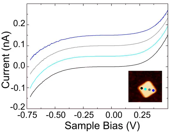
Despite strong similarities between the overall morphology of the NPs, the passivation treatment has a profound effect on the transport measurement performed with scanning tunnelling spectroscopy (STS). When a sequence of I(V) curves is measured on single NPs grown on the etched surface of a p-type InP substrate, we consistently observe the occurrence of a plateau at positive bias, with the onset of the plateau shifted to a higher bias as more and more spectra are acquired (Figure 1d). Conversely, sequences of I(V) curves acquired on single NPs grown on the passivated surface of the same substrate are steadily reproducible and do not show any similar plateau (Figure 1e). Moreover, the reproducibility of the spectra is not only temporal, but also spatial (see Figure S2, SI). While the hysteresis observed on the etched substrate is emblematic of interfacial trapping states,20 the reproducibility of the spectra on the passivated substrate suggests
the absence of charging effect. Hence, we speculate that the different behaviours observed between the etched and the passivated InP substrates are caused by a modification of the interface.
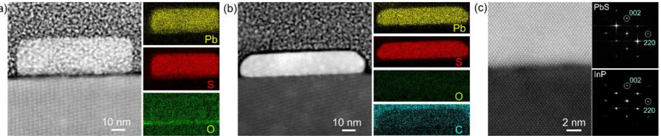
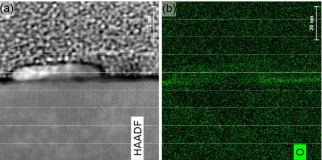
This interface was investigated by combining cross-sectional high angle annular dark field scanning transmission electron microscopy (HAADF-STEM) with energy dispersive spectroscopy (EDS). Although the comparison of thin slices prepared parallel to the {100} edge facets of NPs grown on either the etched or the passivated substrates shows a good crystallinity of the NPs in all cases, an interfacial layer clearly exists between the etched substrates and the NPs. It appears dark in Figure 2a and correspond to an oxygen-rich, amorphous layer. The thickness of this layer is usually inhomogeneous under the NPs (see Figure S3, SI). Depending on the position of the cross-sectional lamellae prepared by focus ion beam, part of the NPs can be found directly in contact with the InP surface, enabling an epitaxial relationship between the InP and PbS lattices, that accounts for the uniformity of the NP orientation on the etched InP surface. In contrast to the NPs grown on this surface, there is no trace of oxygen or carbon species at the interface for the
passivated substrates, demonstrating that the whole base of the NPs is in direct contact with the InP surface (Figure 2b). As the NPs are slightly misoriented in the <100> zone axis, thin slices were also prepared along the {110} diagonal of the NPs. The high resolution STEM image of Figure 2c highlights the abruptness of the interface in the <110> zone axis. Morever, well-matched atomic columns between the InP substrate and the PbS NP are observed, making the fast Fourier transform images acquired in both regions almost superimposable, consistent with the small lattice mismatch of 1.0 % between PbS and InP. Clearly, the passivation of the InP substrates is essential to produce an abrupt and high quality interface and is the origin of the stable and reproducible tunnelling spectra.
Focussing on the PbS NPs that are grown on the passivated InP substrates, we find that the I(V) curves are markedly different depending on the doping of the substrate (Figure 3a). In the case of a p-type passivated InP substrate, all the spectra exhibit a zero-conductance region, whatever the height of the NPs is. This region, labelled Ezc, is better seen when the spectra are plotted on a log
scale. We note that Ezc increases as the NP height decreases. This increase clearly shows up when
a larger set of NPs is probed (Figure 3b) and is related to the increase of the quantum confinement as the height of the NPs decreases.21,22 Surprisingly, the spectra acquired on all the PbS NPs grown
on the n-type InP substrate exhibit a metallic behaviour, even though the confinement is stronger as shown for the two NPs considered in Figure 3a. These characteristics are therefore in contradiction with the semiconductor nature of the PbS NPs.
In order to understand the discrepancy between the p-type and n-type substrates, tight-binding calculations have been performed to determine the band structure of PbS NPs with different heights and infinite lateral sizes.23 The comparison of E
zc with the theoretical band gap shows that
of the I(V) curves reveals a change of the slope at positive bias, that corresponds to an additional onset, labelled ECPbS, and observed above the positive edge of Ezc in the differential conductance
dI(V)/dV for the PbS NPs grown on the p-type InP substrates. No similar behaviour is seen at negative bias. When the energy separation EgPbS between this onset and that of the current at
negative bias (EVPbS) is plotted as a function of the NP height, its variation is found to well fit the
change of the theoretical NP band gap. Therefore, the onset measured at negative bias corresponds to the valence band edge of the PbS NPs and a smaller Ezc indicates that additional empty states
exist below the NP conduction band (CB), in agreement with a type II band alignment in PbS/InP heterojunctions.9
As the spectra acquired on the PbS NPs grown on the n-type InP substrate do not show any quantized effects, we rule out the contribution of the NPs to the tunnelling current at small bias.22
The observation of a metallic behaviour in the spectra also disagrees with the transfer of electrons through trapping states at the PbS/InP heterointerface, which are non-resonant states and should give rise to a negative differential resistance or charging effects.24,25 Hence, we attribute the
tunnelling current at small bias to the pinning of the Fermi level above the CB edge of InP. This is consistent with the existence of a band offset, where the CB edge of PbS is positioned above that of InP. Due to the high doping level of the n-type InP substrate (4.6 x 1018 cm-3), it is possible
not only to directly transfer electrons from the tip states to the InP CB at positive bias, but also to transfer electrons from the occupied states of the InP CB to the tip states at negative bias. In other words, the PbS NPs are electronically transparent in the PbS NPs / n-type InP heterostructures (Figure 3d).
The band offset between the PbS NPs and p-type InP leads to a downward band bending of the InP CB, introducing an inversion layer in InP, that is not dependent on the size of the NPs, due to
the high static dielectric constant of PbS.26 Estimation of the energy of the bound state in the
inversion layer is obtained by first calculating the width of the depletion region (~ 26 nm for an acceptor concentration of 2.8 x 1018 cm-3), then, working out the electrical field in the triangular
well corresponding to the inversion layer (~1MV.cm-1), and finally solving the Schrödinger
equation for this triangular quantum well. If an infinite potential barrier at the interface between PbS and InP is assumed, the bound state is found 0.4 eV above PbS valence edge. Based on the electron affinities of PbS nanocrystals (3.5 eV ~ 4.2 eV)27,28 and InP bulk (4.4 eV),9 the potential
barrier is smaller. Hence, the actual lowering of the potential barrier gives rise to a less confined state, consistent with the measured values of Ezc between 0.17 and 0.37. Again, for bias smaller
than the onset of PbS CB (Figure 3d), electrons directly tunnel from the tip states into the bound state of the p-type InP inversion layer. This tunnelling is allowed for relatively large distances because of the small potential barrier that is encountered by the electrons and the very long de Broglie wavelength in the NPs.
While the photoluminescence experiments are not sensitive to possible radiative transitions between this bound states and critical points of the Brillouin zone in PbS29 due to the existence of
a high concentration of donor to acceptor transitions in p-type InP subtrates (see Figure S4,SI),30
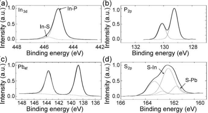
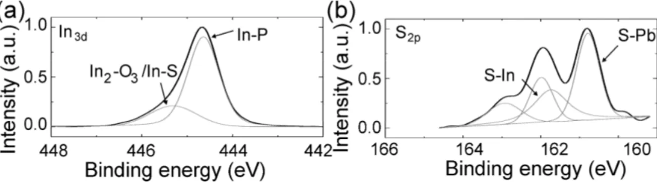
we further studied the quality of the interfaces with photoelectron spectroscopy. For the sample with the thinnest NPs that were obtained on the n-type passivated InP substrate (Figure 4), a weak component shifted by 0.7 eV to a higher binding energy is identified in the In 3d5/2 core level,
indicating the passivation of the In dangling bonds with sulphur atoms.15 Comparison with the In
3d5/2 core level measured for of an etched InP substrate confirms the quality of the passivation,
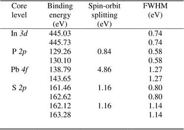
since in this case a broad component is measured and contains both In-S and In-O species (see Figure S6,SI). The surface passivation is additionally supported by the existence of two
components in the S 2p core level, where the strongest component is caused by the In-S bonds, the smallest one being related to the Pb-S bonds in the NPs. The current result is also in agreement with the position of the Fermi level, measured close to the InP conduction band edge in tunnelling spectroscopy (Figure 3(a)) and in photoemission spectroscopy (see Figure S5), corresponding to an optimized sulphur passivation of the surface.31 As no interface component is detected in the P
2p and Pb 4f core levels, the interface appears non-reactive. This is in contrast to the molecular
beam epitaxy of PbS on the reactive InP(001) in ultrahigh vacuum, where lead atoms in a metallic surrounding are found at the interface.32 Interestingly, the measured core levels are comparable
with those measured when an ultrathin epitaxial PbS layer is grown at room temperature on a non-reactive InP (110) substrate by molecular beam epitaxy,33 making the quality of both interfaces
comparable.
CONCLUSION
In conclusion, the direct tunneling of electrons from the STM tip states to the InP CB for energies below the band gap of the PbS NPs demonstrates the absence of electronic traps at the PbS/InP interface. The passivation scheme of the InP substrate prior to the growth of the PbS NPs not only provides an excellent crystalline interface, but also eliminates the interfacial electrically active defects, that degrade the performance of devices prepared by chemical bath deposition. Given the complementary band gaps of PbS and InP, the current PbS/InP heterojunctions produced by CE with trap-free interfaces hold great promise for the fabrication of high-performance semiconductor devices such as photodetectors and solar cells with optical response in a rather broad spectral region from the ultraviolet to infrared. Moreover, since a plethora of semiconductor heterojunctions have already been achieved with CE, the optimization of the chemical treatment
of the host substrates should allow CE to compete on an equal footing with growth techniques performed in vacuum.
METHODS
Sample preparation. The highly polished InP(100) (AXT Inc.) substrates had a thickness of 350µm and were doped either with Zn (p-type) or S (n-type) at a concentration of 2.8 x 1018 cm-3
and 4.6 x 1018 cm-3 respectively. The passivation of the InP surfaces consisted in two steps: first,
the removal of the native oxide layer by immersing them in 1% HF (Sigma) solution, then the sulphur passivation by soaking them into 0.5% (NH4)2S (Sigma) aqueous solution saturated with
sulfur (Sigma) at 60 oC for 1 hr. For the growth of the PbS NPs, the unpassivated and passivated
InP substrates were soaked into a solution containing 1 mM lead acetate (Sigma), 1 mM thiourea (Sigma), 10 ml ethanol (Sigma), and 10 ml ethylene glycol (Sigma) at 95 °C for 1 hr. Lead acetate is the lead source and thiourea is the sulfur source for the formation of PbS crystallites. The pH of the solution was adjusted to 3.4 by adding glacial acetic acid (Sigma). Since phosphine, which is
a very toxic gaz, is generated when InP substrate is treated with acid, this process was
carefully performed in fume hood. After the growth of the PbS NPs, the samples were washed with ethanol and dried with N2 blower.
Scanning Transmission Electron Microscopy. For the investigation of the PbS/InP heterointerface with cross-sectional scanning transmission electron microscopy (STEM), thin lamellae were cut from the samples by focused ion beam and deposited on a specific lift-out copper grid for FIB preparation. They were analyzed by means of HR-STEM and EDXS on a Titan Themis (FEI/Thermo Fischer) microscope operating at 200 keV and equipped with the Super-X
windowless EDX detector (allowing a large detection angle of 0.8 steradian) and a geometric aberration corrector on the probe. The (half)-convergence angle for the probe was 17.6 mrad and the probe current about 70pA. The detection (half)-angles for the HAADF images was between 69 mrad (inner) and 200 mrad (outer).
Scanning tunnelling microscopy. The samples were examined with tungsten tips in a scanning tunnelling microscope working in ultrahigh vacuum (1x10⁻¹⁰ Torr) at a temperature of 77 K.
Tunneling spectroscopic measurements were performed at constant tip-sample separation. The dynamic conductance was measured with a lock-in amplifier using typically 7 mV modulation at 500 Hz on the bias voltage. During the acquisition of a sequence of spectra, ramping the voltage between the sample and the tip took 4.6 s to measure a single spectrum.
Photoluminescence. PbS/InP samples were mounted on a cold finger of a cryostat and were excited non-resonantly using laser diode (photon energy 1.58 eV) focused with a 10 cm lens. The PL was filtered from the scattered laser light with a long pass filter, sent into a 0.55 m spectrometer and detected by a Peletier cooled charged-coupled-device camera.
X-ray photoelectron spectroscopy. The XPS measurements were performed with a monochromatic Al Kα X-ray source and an analyser pass energy of 12 eV. Under these conditions, the overall resolution as measured from the full width at half-maximum (fwhm) of the Ag 3d5/2 line is 0.55 eV. The binding energy scale was calibrated using the Au 4f7/2 line at 84.0 eV. The acceptance angle of the analyser was set to 14°, and the angle between the incident X-rays and the analyser was 90°. The detection angle of the photoelectrons was 45°, as referenced to the sample surface. The intensities of the various XPS core levels were measured as the peak area after standard background subtraction according to the Shirley procedure. For the core level
decomposition, we used Voigt functions and a least squares minimization procedure. The different components were modelled with the same parameters; that is, the Gaussian and Lorentzian broadenings were kept fixed for each component of a given core level.
Tight binding calculations. The electronic structure of PbS NPs with infinite lateral sizes was calculated using a sp3d5s* tight-binding model as described in Ref. 34. The method provides a good
description of the energy gap of spherical PbS quantum dots compared to experiments7.
ASSOCIATED CONTENT
Supporting Information
The following files are available free of charge.
Scanning electron micrograph of PbS nanoplatelets grown on a passivated InP (001) surface; spatially-resolved tunnelling spectroscopy of a PbS NP grown on a p-type passivated InP substrate; photoluminescence of the PbS nanoplatelet / InP (001) heterostructure; valence-band photoemission spectroscopy of a n-type passivated InP (001) substrate with a small density of PbS NPs; fitting parameters of the core levels shown in Figure 4. (PDF).
AUTHOR
INFORMATION
Corresponding Author
Author Contributions
L.B., J.X. and B.G. conceived the experiments. J.H.K. performed the sample preparation. L.B., W.P. A.H., M.Be., B.G. performed the STM/STS characterization. D.R. and Y.L. performed the AFM experiments and the statistical analysis of the NP size. Y.L. and T.X. analysed the samples with SEM. D.T. prepared the TEM samples, that G.P. analysed with STEM. X.W. performed the XPS experiments and analysed the photoemission data with B.G. C.D. performed the tight binding calculations. D.C. and L.B. performed the PL experiments. L.B., X.W., C.D. and B.G. interpreted the data. X.P, M.Ba., J.X. took part in the manuscript writing.
ACKNOWLEDGMENT
This study was financially supported by the European Community’s H2020 Program (Grant No. PITN-GA-2016-722176, “Indeed” Project), the EQUIPEX programs Excelsior (Grant No. ANR-11-EQPX-0015) and Tempos (Grant No. ANR-10-EQPX-0050)), the RENATECH network and the National Key Research and Development Program of China (Grant No. 2017YFA0205700). T. Xu acknowledges the financial support of the National Natural Science Foundation of China (Grant No. 61775130) and J. Xu thanks the University of Lille and ARO for partial financial support. D. Canneson and M. Bayer acknowledge support of the Deutsche Forschungsgemeinschaft in the frame of ICRC TRR 160.
REFERENCES
(1) Lincot, D.; Hodes, G. Chemical Solution Deposition of Semiconducting and Non-Metallic Films: Proceedings of the International Symposium. The Electrochemical Society 2006, 2003-32, 1.
(2) Hodes, G. Semiconductor and Ceramic Nanoparticle Films Deposited by Chemical Bath Deposition. Phys. Chem. Chem. Phys. 2007, 9, 2181-2196.
(3) Osherov, A.; Golan, Y. Chemical Epitaxy of Semiconductor Thin Films. MRS bulletin
2010, 35, 790-796.
(4) McDonald, S. A.; Konstantatos, G.; Zhang, S.; Cyr, P. W.; Klem, E. J.; Levina, L.; Sargent, E. H. Solution-processed PbS Quantum Dot Infrared Photodetectors and Photovoltaics. Nat.
Mater. 2005, 4, 138-142.
(5) Rauch, T.; Böberl, M.; Tedde, S. F.; Fürst, J.; Kovalenko, M. V.; Hesser, G.; Lemmer, U.; Heiss, W.; Hayden, O. Near-infrared Imaging with Quantum-Dot-Sensitized Organic Photodiodes.
Nat. Photon. 2009, 3, 332-336.
(6) Kagan, C. R.; Lifshitz, E.; Sargent, E. H.; Talapin, D. V. Building Devices from Colloidal Quantum Dots. Science 2016, 353, aac5523.
(7). Moreels, I.; Lambert, K.; Smeets, D.; De Muynck, D.; Nollet, T.; Martins, J. C.; Vanhaecke, F.; Vantomme, A.; Delerue, C.; Allan, G.; Hens, Z. Size-dependent Optical Properties of Colloidal PbS Quantum Dots. ACS Nano 2009, 3, 3023-3030.
(8) Chang, C. H.; Lee, Y. L. Chemical Bath Deposition of CdS Quantum Dots onto Mesoscopic TiO2 Films for Application in Quantum-Dot-Sensitized Solar Cells. Appl. Phys. Lett. 2007, 91, 053503.
(9) Liu, Z.; Kim, J. H.; Fernandes, G. E.; Xu, J. Room Temperature Photocurrent Response of PbS/InP Heterojunction. Appl. Phys. Lett. 2009, 95, 231113.
(10) Chang, J. A.; Rhee, J. H.; Im, S. H.; Lee, Y. H.; Kim, H. J.; Seok, S. I.; Nazeeruddin, Md. K.; Gratzel, M. High-performance Nanostructured Inorganic-Organic Heterojunction Solar Cells.
Nano Lett. 2010, 10, 2609-2612.
(11) Chirilă, A.; Reinhard, P.; Pianezzi, F.; Bloesch, P.; Uhl, A. R.; Fella, C.; Kranz, L.; Keller, D.; Gretener, C.; Hagendorfer, H.; Jaeger, D.; Erni, R.; Nishiwaki, S.; Buecheler, S.; Tiwari, A. N. Potassium-induced Surface mModification of Cu(In,Ga)Se2 Thin Films for High-Efficiency Solar
Cells. Nat. Mater. 2013, 12, 1107-1111.
(12) Zhou, Y.; Wang, L.; Chen, S.; Qin, S.; Liu, X.; Chen, J.; Xue, D.-J.; Luo, M.; Cao, Y.; Cheng, Y.; Sargent, E. H.; Tang, J. Thin-film Sb2Se3 Photovoltaics with Oriented
One-Dimensional Ribbons and Benign Grain Boundaries. Nat. Photon. 2015, 9, 409-415.
(13) Xu, X.; Bullock, J.; Schelhas, L. T.; Stutz, E. Z.; Fonseca, J. J.; Hettick, M.; Pool, V. A.; Fai Tai, K.; Toney, M. F.; Fang, X.; Javey, A.; Wong, L. H.; Ager, J.W. Chemical Bath Deposition of p-type Transparent, Highly Conducting (CuS)x:(ZnS)1–x Nanocomposite Thin Films and
Fabrication of Si Heterojunction Solar Cells. Nano Lett. 2016, 16, 1925-1932.
(14) Maman, N.; Templeman, T.; Manis‐Levi, H.; Shandalov, M.; Ezersky, V.; Sarusi, G.; Golan, Y.; Visoly‐Fisher, I. Postgrowth Control of the Interfacial Oxide Thickness in
Semiconductor–Insulator–Semiconductor Heterojunctions. Adv. Mater. Interfaces 2018, 5, 1800231.
(15) Pluchery, O.; Chabal, Y. J.; Opila, R. L. Wet Chemical Cleaning of InP Surfaces Investigated by in situ and ex situ Infrared Spectroscopy. J. Appl. Phys. 2003, 94, 2707-2715.
(16) Wood, B. C.; Schwegler, E.; Choi, W. I.; Ogitsu, T. Surface Chemistry of GaP (001) and InP (001) in Contact with Water. J. Phys. Chem. C 2014, 118, 1062-1070.
(17) Davis, A.; Vaccaro, K.; Dauplaise, H. M.; Waters, W. D.; Lorenzo, J. P. Optimization of Chemical Bath‐deposited Cadmium Sulfide on InP using a Novel Sulfur Pretreatment. J.
Electrochem. Soc. 1999, 146, 1046-1053.
(18) Templeman, T.; Biton, M.; Safrani, T.; Shandalov, M.; Yahel, E.; Golan, Y. Chemically Deposited PbSe Thin Films: Factors Deterring Reproducibility in the Early Stages of Growth.
CrystEngComm 2014, 16, 10553-10559.
(19) Tao, Y., Yelon, A., Sacher, E., Lu, Z. H., Graham, M. J. S‐passivated InP (100)‐(1×1) Surface Prepared by a Wet Chemical Process. Appl. Phys. Lett. 1992, 60, 2669-2671.
(20) Hummon, M. R.; Stollenwerk, A. J.; Narayanamurti, V.; Anikeeva, P. O.; Panzer, M. J.; Wood, V.; Bulović, V. Measuring Charge Trap Occupation and Energy Level in CdSe/ZnS Quantum Dots using a Scanning Tunneling Microscope. Phys. Rev. B 2010, 81, 115439.
(21) Liljeroth, P.; van Emmichoven, P. A. Z.; Hickey, S. G.; Weller, H.; Grandidier, B.; Allan, G.; Vanmaekelbergh, D. Density of States Measured by Scanning Tunneling Spectroscopy Sheds New Light on the Optical Transitions in PbSe Nanocrystals. Phys. Rev. Lett. 2005, 95, 086801.
(22) Diaconescu, B.; Padilha, L. A.; Nagpal, P.; Swartzentruber, B. S.; Klimov, V. I. Measurement of Electronic States of PbS Nanocrystal Quantum Dots using Scanning Tunneling Spectroscopy: the Role of Parity Selection Rules in Optical Absorption. Phys. Rev. Lett. 2013,
110, 127406.
(23) Overgaag, K.; Vanmaekelbergh, D.; Liljeroth, P.; Mahieu, G.; Grandidier, B.; Delerue, C.; Allan, G. Electron-Phonon Coupling and Intervalley Splitting Determine the Linewidth of Single-Electron Transport through PbSe Nanocrystals. J. Chem. Phys. 2009, 131, 224510.
(24) Berthe, M.; Stiufiuc, R.; Grandidier, B.; Deresmes, D.; Delerue, C.; Stiévenard, D. Probing the Carrier Capture Rate of a Single Quantum Level. Science 2008, 319, 436-438.
(25) Rashidi, M.; Taucer, M.; Ozfidan, I.; Lloyd, E.; Koleini, M.; Labidi, H.; Pitters, J. L.; Macieijko, J.; Wolkow, R. A. Time-resolved Imaging of Negative Differential Resistance on the Atomic Scale. Phys. Rev. Lett. 2016, 117, 276805.
(26) Dalven, R. A Review of the Semiconductor Properties of PbTe, PbSe, PbS and PbO.
Infrared Physics 1969, 9, 141-184.
(27) Hyun, B. R., Zhong, Y. W., Bartnik, A. C., Sun, L., Abruna, H. D., Wise, F. W., Goodreau, J. D., Matthews, J. R., Leslie, T. M., Borrelli, N. F. Electron Injection from Colloidal PbS Quantum Dots into Titanium Dioxide Nanoparticles. ACS nano 2008, 2, 2206-2212.
(28) Wang, X., Koleilat, G. I., Tang, J., Liu, H., Kramer, I. J., Debnath, R., Brzozowski, L., Barkhouse, A. R., Levina, L., Hoogland, S., Sargent, E. H. Tandem Colloidal Quantum Dot Solar Cells Employing a Graded Recombination Layer. Nat. Photon. 2011 5, 480-485.
(29) Geiregat, P.; Delerue, C.; Justo, Y.; Aerts, M.; Spoor, F.; Van Thourhout, D.; Siebbeles, L. D. A.; Allan, G.; Houtepen, A. J.; Hens, Z. A Phonon Scattering Bottleneck for Carrier Cooling in Lead Chalcogenide Nanocrystals. ACS nano 2015, 9, 778-788.
(30) Swaminathan, V.; Donnelly, V. M.; Long, J. A Photoluminescence Study of Cd‐related Centers in InP. J. Appl. Phys. 1985, 58, 4565-4572.
(31) Bessolov, V. N.; Lebedev, M. V.; Zahn, D. R. T. Surface of n-type InP (100) Passivated in Sulfide Solutions. Semiconductors 1999, 33, 416-420.
(32) Preobrajenski, A. B.; Chasse, T. Atomic and Electronic Structure of Epitaxial PbS on InP (110) and InP (001). Appl. Surf. Sci. 2000, 166, 201-208.
(33) Preobrajenski, A. B.; Chasse, T. Epitaxial Growth and Interface Structure of PbS on InP (110). Appl. Surf. Sci. 1999, 142, 394-399.
(34) Allan, G., Delerue, C. Confinement Effects in PbSe Quantum Wells and Nanocrystals.
FIGURE 1. (a) Scanning electron micrograph of PbS nanoplatelets grown on an InP (001) surface after removal of the native oxide with a buffer oxide etchant. (b) Schematic of two different InP surfaces prepared for the growth of the PbS nanoplatelets (NPs). (c) Statistical analysis of the NP top facet area versus their height measured with STM and AFM. The NPs were grown after the sulphur passivation of the InP surface. Inset: (left) Scanning electron micrograph of the nanoplatelets and (right) three-dimensional view of the nanoplatelets observed with AFM with an amplified z-scale. (d) Sequences of eleven tunnelling spectra acquired on PbS NPs grown on an p-type etched InP (001) surface. The arrow points towards the direction of the potential shift as the acquisition of spectra proceeds. (e) Sequences of eleven tunnelling spectra acquired on PbS NPs grown on a p-type passivated InP (001) surface. Tunneling conditions at 77K: Vsample =-1.0 V,
FIGURE 2. (a) (100) cross-sectional high-angle annular dark-field (HAADF) scanning transmission electron microscopy (STEM) image of a nanoplatelet grown on an etched InP (001) surface and related energy-dispersive spectrometer (EDS) mapping images for Pb, S and O. (b) (100) cross-sectional HAADF-STEM image of a nanoplatelet grown on a passivated InP (001) surface and related EDS mapping images for Pb, S, O and C. (c) High resolution (1-10) cross-sectional HAADF-STEM image of the PbS/S-passivated InP interface and corresponding Fast Fourier transforms (FFT) of the image acquired in the PbS (top) and InP (bottom) areas.
FIGURE 3. (a) Constant current STM images of PbS nanoplatelets (NPs) grown either on the p-type or n-p-type passivated InP substrates and related I(V) spectra (Tunnelling current It = 8 pA,
sample voltage VS = -5 V, temperature of 77K). The scale bars correspond to 80 nm. Reference
I(V) curves measured on NP-free areas of the n-type and p-type InP substrates are also shown. Ezc,
indicates the width of the zero-conductance region (red arrows), EF the Fermi level position, EVPbS
the valence band edge and ECPbS the conduction band edge of the PbS NPs respectively. h
corresponds to the height of the NPs. The spectra have been shifted for clarity. (b) Variations of Ezc and of the measured band gap EgPbS of PbS as a function of h. The experimental data are
compared with the theoretical band gap of PbS sheets with similar heights but infinite lateral size as determined with tight binding calculations. (c) dI/dV(V) spectra of the PbS NPs shown in (a) that were grown on the p-type InP substrate. ECPbS indicates the position of the conduction band
edge of the PbS NPs. EVPbS corresponds to the top of the valence band edge of the NPs.(d) (left)
a quantum level positioned at an energy Ezc above the top of the PbS valence band for a p-type
substrate. The horizontal arrow indicates the direct tunnelling of electrons from the tip into this quantum level. In the PbS NPs, the Fermi level is positioned closer to the valence band edge based on the tunnelling spectra measured in (a). (right) Band diagram of the PbS/InP heterostructure for a n-type substrate. The InP valence and conduction bands and the applied bias are labelled VB, CB and V respectively.
FIGURE 4. Photoelectron spectra of the (a) In 3d (b) P 2p, (c) Pb 2p and (d) S 2p core levels measured for a small density of PbS nanoplatelets grown on a n-type passivated InP (001) surface. The thin lines correspond to fits obtained with the parameters given in Table S1, SI.
Supporting information
Trap-Free Heterostructure of PbS Nanoplatelets on InP(001) by
Chemical Epitaxy
Louis Biadala†, Wenbing Peng†,‡, Yannick Lambert†, Jin H. Kim§, Damien Canneson‖, Anthony
Houppe†,┴, Maxime Berthe†, David Troadec†, Dominique Deresmes†, Gilles Patriarche#, Tao Xu†,¶,
Xiaodong Pi‡, Xavier Wallart†, Christophe Delerue†, Manfred Bayer‖, Jimmy Xu§, Bruno Grandidier†*
† Univ. Lille, CNRS, Centrale Lille, ISEN, Univ. Valenciennes, UMR 8520 - IEMN, F-59000 Lille, France
‡ State Key Laboratory of silicon Materials, and School of Materials Science and Engineering, Zhejiang University,
Hangzhou, Zhejiang 310027, China.
§ School of Engineering, Brown University, Providence, Rhode Island 02912, USA. ‖
Experimentelle Physik 2, Technische Universität Dortmund, 44221 Dortmund, Germany.
┴ Département de physique de l’ENS, Ecole Normale Supérieure, PSL Research University, Université Paris Diderot, Sorbonne Paris Cité, Sorbonne Universités, UPMC Université Paris 06, CNRS, 75005 Paris, France.
# Centre de Nanosciences et de Nanotechnologies (C2N), UMR 9001 CNRS, University Paris Sud, University
Paris-Saclay, avenue de la Vauve, 91120 Palaiseau, France.
¶ Key Laboratory of Advanced Display and System Application, Shanghai University, 149 Yanchang Road, Shanghai
200072, People’s Republic of China.
*Email: bruno.grandidier@isen.iemn.univ-lille1.fr
Table of contents
• Figure S1. Scanning electron micrograph of PbS nanoplatelets grown on a passivated InP (001) surface.
• Figure S2. Spatially-resolved tunnelling spectroscopy of a PbS NP grown on a passivated p-type InP substrate.
• Figure S3. (100) cross-sectional high-angle annular dark-field (HAADF) scanning transmission electron microscopy (STEM) image of a PbS NP grown on an etched InP (001) surface and related energy-dispersive spectrometer (EDS) mapping image for O.
• Figure S4. Photoluminescence of the PbS nanoplatelet / InP (001) heterostructure.
• Figure S5. Photoelectron spectra of the (a) In 3d and (b) S 2p core levels measured for PbS nanoplatelets grown on a p-type etched InP (001) surface.
• Figure S6. Valence-band photoemission spectroscopy (top) of PbS NPs grown on a p-type etched InP (001)
surface and (bottom) of a n-type passivated InP (001) substrate with a small density of PbS NPs.
Figure S1. Scanning electron micrograph of PbS nanoplatelets grown on a passivated InP (001) surface. The SEM image is the same as the one shown in the inset of Figure 1c. Its bigger size highlights the formation of the smallest nanoplatelets.
Figure S2. Spatially-resolved tunnelling spectroscopy of a PbS NP grown on a passivated p-type InP substrate. Tunneling conditions at 77K: Vsample =-0.6 V, Isetpoint =70 pA. Inset: STM image of the NP showing
Figure S3. (100) cross-sectional high-angle annular dark-field (HAADF) scanning transmission electron microscopy (STEM) image of a PbS NP grown on an etched InP (001) surface and related energy-dispersive spectrometer (EDS) mapping image for O.
Figure S4. Photoluminescence of the PbS nanoplatelet / InP (001) heterostructure. (a) Comparison of PL spectra between PbS nanoplatelets grown on passivated n-type and p-type InP substrates. The spectra have been shifted for clarity. (b) Excitation intensity dependence of the PL spectrum for the PbS nanoplatelets grown on the passivated p-type InP substrate. The low and high energy bands are labelled LEB (low energy band) and HEB (high energy band) respectively. (c) Peak photon energies of the low energy bands as a function of the excitation power, that is caused by donor-acceptor pair transitions.
Figure S5. Photoelectron spectra of the (a) In 3d and (b) S 2p core levels measured for PbS nanoplatelets grown on a p-type etched InP (001) surface. The main peak positions obtained from the decomposition of the core levels are shifted by 0.65eV with respect to the ones found for the n-type passivated sample of Figure 4, consistent with the shift of the Fermi level shown in Figure S5.
Figure S6. Valence-band photoemission spectroscopy (top) of PbS NPs grown on a p-type etched InP (001) surface and (bottom) of a n-type passivated InP (001) substrate with a small density of PbS NPs.
Table S1. Fitting parameters of the core levels shown in Figure 4. Core level Binding energy (eV) Spin-orbit splitting (eV) FWHM (eV) In 3d 445.03 0.74 445.73 0.74 P 2p 129.26 0.84 0.58 130.10 0.58 Pb 4f 138.79 4.86 1.27 143.65 1.27 S 2p 161.46 1.16 0.80 162.62 0.80 162.12 1.16 1.14 163.28 1.14